Abstract—This paper describes a new band-gap reference (BGR) without resistors that can be fabricated in a 0.35μm digital CMOS technology. The proposed circuit uses differential amplifier to reduce the current mirror errors dependent on the supply voltage and temperature, so as to produce a temperature insensitive gain applied to the proportional to absolute temperature (PTAT) term in the reference. The simulation results with Spice indicate that the proposed BGR circuit has a higher power supply rejection ratio (PSRR) and low temperature coefficient (TC). The fluctuation of the output reference voltage is less than 9 mV when the power voltage changes from 2.4V to 5.0V and the output voltage of the new circuit has a maximum variation of ± 5.5 mV in larger range from -25 to 125℃.
Index Terms—BGR without resistors, differential amplifier, digital process, self-biased circuit, PTAT voltage.
I. INTRODUCTION
Reference voltage generators with low sensitivity to the temperature and supply are commonly required both in analog and digital circuits, such as data-conversion systems, voltage regulators and memories, because of its good temperature stability and insensitivity to supply voltage. The basic idea of BGR in CMOS technology is to add a PTAT voltage to emitter-base voltage (VBE) of a parasitic pnp transistor. In order to generate a quantity Vref that remains constant with temperature, the circuit should implement two voltages that have positive and negative temperature coefficients. Then add them with proper weighting [1], as shown in Fig.1.
Figure 1 The principle of BGR
The VBE of bipolar transistors or, more generally, the forward voltage of a p-n junction diode exhibits a negative TC. While the difference between VBE of two bipolar transistors operate at unequal current densities (ΔVBE ) is directly proportional to the absolute temperature.
In conventional BGR circuit, the output voltage is usually achieved by adjusting the ratio of resistors. However, in a Manuscript received September 6, 2007.
Yujiao Zhao, Suge Yue and Qiang Bian ,
Beijing Microelectronics Technology Institute, Beijing, 100076, China. E-Mail:[email protected]
standard digital CMOS process, the presence of resistors is a drawback for some applications. As we know the resistivity is not guaranteed by some foundries and can vary with the process. Also, in a digital process, the area of such resistors is increased because silicide is often used to reduce the sheet resistance of the poly-silicon and diffusion layers. The BGR described in [2] gave a good solution to the above problems: a band-gap reference without resistors. This solution eliminates the need for resistor models .But as we can see, the PSRR of the circuit isn’t very high and the output voltage has a greater variation with temperature. On the other hand, in order to reduce the effect of channel length modulation, all the transistors have long channel length that increases the area evidently.
In this paper, a new BGR circuit without resistors is proposed. We improve the power supply rejection and eliminate the TC by using differential amplifier which reduces the current mirror errors due to the variation of the supply voltage and temperature. The BGR described uses MOS transistors only biased in saturation or cutoff, for which accurate device models are usually available, simplifying the design process, especially in digital CMOS technologies.
II. PRINCIPLE OF BAND-GAP REFERENCE CIRCUIT WITHOUT RESISTORS
The core circuit shown in Fig.2 allows integrating a BGR without using resistors [3].
Figure 2 Schematic of the core of the resistorless band-gap reference
As shown in Fig.1. BE BE
Vref =V + Δk V (1)
A Novel Low Temperature Coefficient Band-gap
Reference without Resistors
Yujiao Zhao, Suge Yue, Qiang Bian
Proceedings of the International MultiConference of Engineers and Computer Scientists 2008 Vol II IMECS 2008, 19-21 March, 2008, Hong Kong
Vref is the output reference voltage. In the conventional BGR circuit [1], the reference voltage is the sum of the built-in voltage of the diode and the thermal voltage multiplied by a constant factor. Since in this circuit (shown in Fig.2) resistors are not used, the required constant factor is obtained by using radioed transistors together with the inverse function technique.
The PTAT voltage ΔVD = VD2 - VD1 is applied across the
differential pair M1~M2, the resulting current is multiplied by G using current mirror M5~M6 and is delivered to the differential pair M3~M4. Suppose that all the transistors M1~M4 operate in the saturation region, neglecting channel-length modulation and body effect, the circuit can be analyzed using a simple square-Law MOS model.
We have 2 1 2 1 2 1 2 2 ( / ) ( / ) DS DS GS GS I I
kp W L kpW L
V −V = − (2)
4 3 4 3 4 3 2 2 ( / ) ( / ) DS DS GS GS I I
kp W L kp W L
V −V = − (3) Where kp =μpCox, μp is the mobility of carrier,Cox is the gate oxide capacitance per unit area.
In the circuit, (W/L)6 =G(W/L)5, So
4 2
DS DS
I =GI ,
Since
2 1
DS DS T
I +I =I ,
4 3
DS DS T
I +I =GI .
3 4 4 1
DS T DS T DS DS
I =GI −I =GI −GI =GI .
From equations (3) and (4),
2 1 2 1 2 2 ( / ) ( / ) DS DS GS GS I I
k AB W Lp k A W Lp
V −V = − (4)
2 1 4 3 2 2 ( / ) ( / ) DS DS GS GS GI GI
k AB W Lp k A W Lp
V −V = −
2 1
( )
GS GS AG V V
= − (5) As shown, M1and M2, M3and M4 connected in source, we could get the PTAT voltage
2 1
GS GS D
V −V = ΔV , 2
1
2 1 ln
D
D
D D D T
I
I
V V −V V
Δ = = ,
VT is the thermal voltage. Then
2
out D AG D
V =V + ΔV (6) It is known, by choosing A, G and n, the zero TC voltage could be achieved at room temperature.
A CMOS BGR without resistors was presented [2]. It is obviously that the bias current is important for the performance of the circuit. In this circuit, the bias current is provided using bootstrapped structure of little supply dependence (but still a function of process and temperature). At the same time, in order to neglect channel-length modulation, relatively long channels are used for all the transistors in the circuit. And this increases the area evidently.
III. IMPROVED VOLTAGE REFERENCE
In this section, we will describe the alternative solution having a much higher power supply rejection and better temperature coefficient. The band-gap reference presented in
this paper uses an amplifier, which is biased by the output of the circuit itself, forming feedback loop, to generate accurate self-biased current. And this improves the performance of the band-gap reference, such as TC, PSRR.
A. PTAT Voltage Generation Circuit Composed of
Differential Amplifier
First, let’s consider the circuit generating the PTAT voltage in Fig.3. A self-biased circuit including amplifier was presented, allowing the stable biasing current for Q1 and Q2.
Figure 3 PTAT voltage generation circuit
The emitter area of Q1 is n (n>1) times larger than the emitter area of Q2 and the width of M2 is m (m>1) times bigger than the width of M1, where as their lengths are equal. M3~ M5and M6, M7, M9 are identical separately. M8is twice of the M6. By using differential amplifier, M1 and M2 have the same threshold voltages and systematic mismatch is reduced, making the drain-source voltages as closed to equal as possible. So the currents through Q1, Q2, M1 and M2 have same value I. It is obviously, the amplifier eliminates the effects of channel-length modulation and body effect and the feedback loop could also decrease the variation of current I. From sectionⅡ, it is easy to get the PTAT voltage
2 1 ln( )
GS GS D
kT q
V −V = ΔV = n (7) The structure of the differential amplifier shown in Fig.3 is viewed in Fig.4.
Figure 4 Implementation of differential amplifier
Proceedings of the International MultiConference of Engineers and Computer Scientists 2008 Vol II IMECS 2008, 19-21 March, 2008, Hong Kong
Figure 5 Complete circuit of the proposed BGR
B. Proposed BGR Circuit
The technique employs amplifier (composed of M9~M12, shown in Fig.4) to force VDSof M5 and M6 to be to be equal. The feedback loop is the key of the proposed circuit. When temperature changes, the voltage of M9 gate equaling to VBE2 also changes. The changing of the output voltage of amplifier will vary the bias current to minus the variation of
VBE of the two pnp parasitic transistor. From equation (7), by connecting similar configuration to the gate of M2, we can obtain the voltage reference. The implementation circuit is shown in Fig.5. In order to improve the precision and PSRR of the reference farther, a cascade current mirror is introduced to the final reference circuit. The emitter area of Q1 is 32 times bigger than the emitter area of Q2 and the width of M2 is 2 times bigger than the width of M1. M3 and M4 have same sizes with M1 and M2, while M18 and M24 have larger W/L as 15 times as M16 and M21, so currents through M3 and M4 are enlarged by 15 times. The amplifier eliminates the effects of channel-length modulation and body effect, so all NMOS of this circuit could have minimum length, the area of the circuit obviously. In this way, adding the two voltages that have positive and negative temperature coefficients with, Vref is generated with zero TC at chosen temperature (this paper, the temperature is 75℃).
C. Start-up Circuitry
To ensure that the BGR circuit works in the correct state, a start-up circuit must be added [4]. The startup circuit is formed by M25~M28 (see Fig.5). When the circuit operates, the gate voltage of M26is pulled low, and this turns on M26. So the gate voltage of M13 is pulled high, and this turns on M19. Because of the current mirror, M14~ M25are all turned on and inject current to the amplifier. M25 is turned on, so the gate voltage of M26 is pulled high, transistor M26 is turned off. The start-up circuit is cut off, when the reference circuit works normally.
Ҋ. SIMULATION RESULTS
The performances of the proposed band-gap reference are verified through Spice simulation with a 0.35-μm CMOS process model.
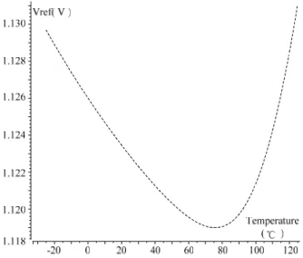
With a supply voltage 3.3 V and temperature from the range of -25 to 125℃, the simulated output voltage of the proposed BGR as a function of temperature is shown in Fig. 6. The output voltage has a maximum variation of ± 5.5 mV from the mean output voltage of 1.124V.
Figure 6 Output voltage of band-gap reference as a function of temperature with supply voltage to be 3.3 V
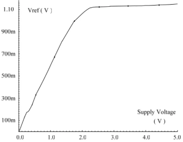
The simulated output voltage of the proposed circuit as a function of supply voltage is shown in Fig. 7. The fluctuation of the output reference voltage is about 9 mV when the power voltage changes from 2.4V to 5V. The simulated PSRR is shown in Fig. 8 to check the behavior of the output voltage with variation of frequency. The PSRR for frequencies below 1 KHz is -49.2 dB and increases to about -28dB at 1 MHz.
Proceedings of the International MultiConference of Engineers and Computer Scientists 2008 Vol II IMECS 2008, 19-21 March, 2008, Hong Kong
Figure 7 Output voltage of the band-gap reference as a function of the supply voltage at room temperature
Figure 8 PSRR of the band-gap reference
The comparison in Tabel.1 shows the proposed circuit (the simulation result is noted with *) achieves better TC with extending temperature operating range and good line regulation.
Table 1
ҋ. CONCLUSION
A novel voltage band-gap reference circuit without resistors has been proposed in this paper and simulated with 0.35-μm CMOS process. The differential amplifier is applied to forming self-biased circuit which can provide more accurate bias current for the whole BGR circuit. The simulation results indicate that the applying of amplifier improves PSRR and reduces TC effectively. In addition, because of amplifier, all NMOS of this circuit could have minimum length, which decreases area of the circuit obviously.
REFERENCES
[1] B.Razavi, McGraw- Hill, “ Design of Analog CMOS Integrated Circuits”, 2001. pp. 377–392.
[2] A.Buck, C. Mc Donald, S. Lewis, T.R. Viswanathan, “A CMOS bandgap reference without resistors”,in Journal of Solid State Circuits, vol. 37, no. 1 January 2002.
[3] A. Buck, C. McDonald, S. Lewis, and T. R. Viswanathan, “A CMOS bandgap reference without resistors,” in IEEE Int. Solid-State Circuits Conf. Dig. Tech. Papers, Feb. 2000, pp. 442–443.
[4] Ka Nang Leung and Philip K. T. Mok, “A CMOS Voltage Reference Based on Weighted Difference of Gate-Source Voltages between PMOS and NMOS Transistors for Low Dropout Regulators”, Solid-State Circuits Conference, Sept. 2001
[5] Cheng Jianping,Zhu Zhuoya, Wei Tongli, “A resistorless CMOS bandgap reference with below 1V output” , Journal of Southeast University, vol.19, no. 4 December 2003.
[6] Ahmet Tekin , Ertan Zencir, et al, “A Bias Circuit Based on Resistorless Bandgap Reference in 0.35-μm SOI CMOS”, vol.1, 149-152, Dec. 2003,IEEE
[7] Christian Falconi, Giuseppe Scotti, “Low Voltage CMOS Current and Voltage References without Resistors”, May 2007, IEEE,
pp.1907-1910.
Proceedings of the International MultiConference of Engineers and Computer Scientists 2008 Vol II IMECS 2008, 19-21 March, 2008, Hong Kong