Strain relaxation and stress-driven interdiffusion in In As In Ga As In P nanowires
L. Nieto, J. R. R. Bortoleto, M. A. Cotta, R. Magalhães-Paniago, and H. R. Gutiérrez
Citation: Applied Physics Letters 91, 063122 (2007); doi: 10.1063/1.2764446
View online: http://dx.doi.org/10.1063/1.2764446
View Table of Contents: http://scitation.aip.org/content/aip/journal/apl/91/6?ver=pdfcov
Published by the AIP Publishing
Strain relaxation and stress-driven interdiffusion in InAs / InGaAs / InP
nanowires
L. Nieto, J. R. R. Bortoleto,a兲 and M. A. Cottab兲
Instituto de Física Gleb Wataghin, UNICAMP, CP 6165, 13083-970 Campinas, São Paulo, Brazil
R. Magalhães-Paniago
Departamento de Física, UFMG, CP 702, 30123-970 Belo Horizonte, Minas Gerais, Brazil
H. R. Gutiérrez
Department of Physics, Pennsylvania State University, University Park, Pennsylvania 16802-6300
共Received 23 May 2007; accepted 3 July 2007; published online 9 August 2007兲
The authors have investigated strain relaxation in InAs/ InGaAs/ InP nanowires 共NW’s兲. Transmission electron microscopy images show an additional stress field attributed to compositional modulation in the ternary layer, which disrupts NW formation and drives Ga interdiffusion into InAs, according to grazing incidence x-Ray diffraction under anomalous scattering conditions. The strain profile along the NW, however, is not significantly affected when interdiffusion is considered. Results show that the InAs NW energetic stability is preserved with the introduction of ternary buffer layer in the structure. ©2007 American Institute of Physics.关DOI:10.1063/1.2764446兴
Considerable amount of work has been carried out on self-assembled quantum dots and wires due to the attractive physical properties expected from these nanostructures.1 In particular, InP-based InAs nanostructures are also interesting for their ability to work as light emitters in the 1.30– 1.60m long-wavelength region.2–7In contrast to the
InAs/ GaAs system, the formation process of InAs nano-structures on InP substrates is characterized by the lower strain 共⬃3.2%兲 between InAs and the buffer layers, and complicated by possible chemical alloying with the substrate,2,3anisotropic stress relaxation,7and the large num-ber of possible materials for the buffer layer.2–7Experimental results suggest that stress relaxation7 and/or the chemical composition4 of the buffer layer 共InP, InAlAs, or InGaAs兲 have key roles in configuring the final shape of the InAs nanostructures. However, the mechanism associated with the formation of a specific surface morphology of nanostructures still remains under discussion.8
In this letter, we analyze the role of InGaAs/ InP buffer layers grown under different conditions on InAs nanowires 共NW’s兲shape and size. Our results suggest that InGaAs com-positional modulation disrupts the formation of InAs NW’s due to the associated periodic stress field. When the modu-lation is not present, strain relaxation in InAs/ InGaAs NW’s is very similar to the InAs/ InP case, suggesting a minor role for using a different buffer layer.
The samples were grown on vicinal 共2° off towards 具111典A兲 共001兲InP substrates by chemical beam epitaxy. A 120 nm thick InP buffer layer was deposited followed by the nominally lattice-matched InGaAs film, with thickness vary-ing between 10 and 100 nm and a planar surface for the subsequent InAs growth at 490 ° C and 2.4 Å / s. The main differences regarding sample structure are due to InGaAs thickness共12 nm for sample B and 100 nm for samples C and D兲and As2overpressure during InGaAs growth共a
three-fold overpressure was used for sample D as compared to B and C兲. Sample A is a reference sample where InAs was deposited directly on InP. All samples were cooled down in vacuum in order to preserve the actual nanostructure shape9 and analyzed by in-air atomic force microscopy共AFM兲and cross sectional transmission electron microscopy共TEM兲 us-ing a JEM 3010 URP 300 kV. Nanowire strain relaxation was investigated by the grazing incidence x-ray diffraction 共GIXD兲.10,11 We have used GIXD radial and angular scans under anomalous scattering conditions12in order to evaluate the presence of Ga within the InAs nanostructures. The dif-ference in intensity between radial scans for the 共2–20兲 re-flection taken at 10 keV 共I2兲 and at the K-edge absorption energy for Ga,E= 10.367 keV共I1兲 provided the Ga concen-tration in the nanostructure,12according to
CGa=1 2共f
In+fAs兲 1 −
冑
I1/I2冑
I1/I2共f2Ga−fIn兲−共f1Ga−fIn兲. 共1兲where the In and As scattering factors fare constant at the energies used,CIn+CGa= 0.5 andCAs= 0.5. Subsequently, an-gular scans at the Ga K-edge energy as well as TEM and AFM images11–13allowed us to create a profile of the actual Ga concentration along the height of the InAs NW.
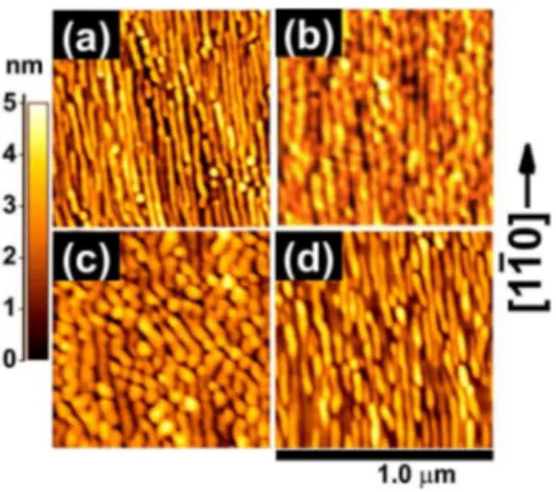
Figure 1 shows AFM topographies of the InAs NW’s. We can observe that InAs/ InP wires 关Fig.1共a兲, sample A兴 run quite uniformly along the 关1 − 10兴 direction with base width ⬃32 nm. However, for sample B, where InAs was grown on an ⬃12 nm thick InGaAs film 关Fig. 1共b兲兴, the NW’s are usually shorter, with a few dots showing up on the surface. In this case, the NW base width is ⬃45 nm. The shape of the NW’s is altered even further when the thickness of the InGaAs film is increased to 100 nm 共sample C兲, as shown in Fig.1共c兲. In this case, the NW shape anisotropy is also altered, and tilted structures—as compared to the previ-ous images—show up on the surface. However, Fig. 1共d兲 shows that it is possible to regain InAs/ InGaAs shapes simi-lar to InAs/ InP共sample D兲. In this case, the InGaAs thick-ness is also ⬃100 nm, and the only difference in growth conditions is the larger As2overpressure. The InAs NW’s are
a兲Present address: Campus Experimental de Sorocaba, GPM, UNESP, Soro-caba, 18087-180 São Paulo, Brazil.
b兲Electronic mail: [email protected]
APPLIED PHYSICS LETTERS91, 063122共2007兲
0003-6951/2007/91共6兲/063122/3/$23.00 91, 063122-1 © 2007 American Institute of Physics
more regular and uniform, similar to those grown on InP, and the base width dropped to⬃35 nm. The density and height distribution of the NW’s also varies depending on InGaAs growth conditions.
The formation of InAs NW’s on InP has been attributed to InP surface anisotropy14 and to anisotropic stress relax-ation linked to the P–As interface.7However, InAs NW’s on InGaAs/ InP have already been reported.5 In our case, we observe that the shape and direction of the NW’s on the surface depends on the buffer layer thickness, suggesting the role of a volumetric effect. This effect could be attributed to different elastic properties of InGaAs and InP films. Thin InGaAs films would not hinder completely the presence of the InP substrate underneath. However, elastic parameters for these materials are very similar and could not explain the observed behavior. Moreover, this effect would not be sup-pressed by changing InGaAs growth conditions, as shown in Fig.1共d兲.
Figure 2 shows g=共−2 − 20兲 dark field TEM images of samples B, C, and D. An intensity contrast in the InGaAs layer can be seen in Figs. 2共a兲 and 2共b兲; this contrast is periodically more uniform and clear along the layer for the thicker InGaAs film. These results can be associated with the compositional modulation within the InGaAs film, most likely due to the low As2 overpressure used.15–17 A two-dimensional periodic pattern along the关100兴and关010兴 direc-tions for In and Ga rich regions has been reported for com-positionally modulated III-V layers.16–18If this is the case for our InGaAs films, the modulation strain field will be rotated 45° from the关1 − 10兴 direction of the InAs/ InP NW’s long axis.14 From TEM, we estimate the period of the composi-tional modulation inside the InGaAs layer of samples B and C in the range of 45– 50 nm. These values are similar to the
NW base width for these samples. Moreover, we can observe in Fig. 1共c兲 that NW’s are more discontinuous and often oriented at about 45° out of关1 − 10兴direction. Larger group V overpressures usually hinder the formation of composi-tional modulation in ternary layers.16Indeed, the TEM image of sample D关Fig.2共c兲兴shows only the contrast usually as-sociated with the strain field of the InAs nanostructures.
The periodic strain field associated with the modulation may disrupt the formation of InAs NW’s since it represents an extra driving force for In diffusion along the surface. As a result, InAs accumulates on top of In-rich regions on the InGaAs surface, especially for the first few layers, which will eventually determine the onset of three-dimensional island-ing. For thin InGaAs films, where the stress field is weaker, the main result is the altered aspect ratio of InAs NW’s, with a larger base width. For a thicker InGaAs buffer layer, how-ever, both shape and direction of the nanostructures on the surface are affected.
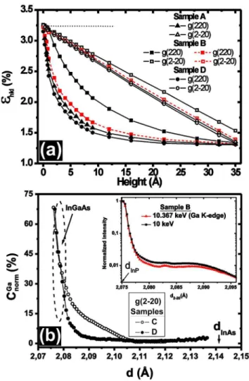
Figure 3共a兲 shows the anisotropic strain relaxation for NW’s grown on InGaAs and InP. We have plotted the strain hkl=共dInAs−dhkl兲/dInAsas a function of the height of the NW along both the关220兴and关2 − 20兴 directions. The height val-ues in the figure were calculated considering the NW base width 共obtained by GIXD and TEM兲 and 兵114其 sidewall facets,11 still preserved when InAs is deposited on InGaAs. The curves for samples A and D are very similar. The InAs NW grown on InGaAs共sample D兲relaxes slightly faster than for InAs/ InP共sample A兲. Anomalous scans taken at the Ga
K-edge energy show no sign of Ga interdiffusion from In-GaAs into the InAs NW’s for sample D 关Fig. 3共b兲兴. These results suggest that the InAs strain relaxation should not strongly depend on the buffer material.
A completely different result, however, is obtained for sample B, where the shape of the NW’s is still preserved in spite of the compositional modulation observed in the In-GaAs buffer layer. In this case, GIXD data taken at 10 keV 关Fig.3共a兲兴indicate that strain relaxation—especially for the 关220兴 direction—is quite different from the previous case. However, anomalous radial scans, shown in the inset of Fig. 3共b兲, indicate a non-negligible Ga concentration within the InAs NW’s for this sample. The Ga profile obtained using angular scans is shown in Fig.3共b兲. This result suggests that interdiffusion takes place due to the extra strain field pro-vided by compositional modulation. Once a nanometer-sized, two-dimensional periodic strain field is built in the buffer layer, strain-driven kinetic processes can take place during InAs deposition. The relatively fast growth rates for InAs used here should not account for Ga surface diffusion as the origin of the observed behavior. Keeping in mind that the NW long axis should be rotated with regard to the modula-tion pattern,17we can assume that sections of the InAs NW’s are deposited on Ga-rich regions of the buffer layer, thus providing the driving force for Ga interdiffusion.
FIG. 1.共Color online兲AFM images of InAs NW’s.共a兲InAs/ InP共sample A兲
and InAs/ InGaAs/ InP with InGaAs thickness共b兲 12 nm共sample B兲, 共c兲
100 nm共sample C兲, and共d兲100 nm, grown under larger As2overpressure
共sample D兲. The heights and NW’s densities depend on growth condition and thickness of the InGaAs buffer layers. However, samples A and D共B and C兲show similar height distributions.
FIG. 2. High resolution TEM关dark field forg=共−2 − 20兲兴 cross section images of InAs/ InGaAs NW’s. Bright and dark re-gions in InGaAs show typical mass con-trast associated with compositional modu-lation in samples共a兲B,共b兲C, and共c兲D.
063122-2 Nietoet al. Appl. Phys. Lett.91, 063122共2007兲
The Ga profiles shown in Fig.3共b兲reflect an average of the NW strain field probed by GIXD measurements. If we then recalculate the strain curve along the height of the nano-structure, assuming a Vegard law for the In共Ga兲As lattice parameter at each isostrain plane, we obtain the dashed curve, shown in Fig. 3共a兲, where hkl=共dInxGa1−xAs−dhkl兲/ dIn
xGa1−xAs. We can notice that the actual strain for sample B
is very similar to those from samples A and D, small differ-ences likely related to the NW shape variations. Also, in the
case of sample B, local Ga variations must exist within the NW’s, which cannot be probed by GIXD.
In summary, the formation of InAs NW’s on InGaAs/ InP, under certain growth conditions, depends on the thickness of the InGaAs buffer layer. Our results suggest that compositional modulation in the buffer layer disrupts nanowire formation and may lead to Ga interdiffusion. The strain relaxation profile along the nanostructure, however, is very similar to the InAs/ InP case if the modulation is not present in the buffer layer or the actual Ga concentration is considered. Our results show that the introduction of a ter-nary compound in between InAs/ InP does not significantly affect InAs NW stability if proper parameters are chosen for the growth. This nanostructure stability is a suitable charac-teristic for band gap engineering and device applications.
One of the authors 共L.N.兲 acknowledges scholarship from CNPq. This work was supported by FAPESP and CNPq. HRTEM and GIXD measurements were performed at LME and XRD-2 station, respectively, at the National Labo-ratory of Synchrotron Light共LNLS, Brazil兲.
1A. D. Yoffe, Adv. Phys. 50, 1
共2001兲.
2J. Brault, M. Gendry, G. Grenet, G. Hollinger, Y. Dieres, and T.
Benyattou, Appl. Phys. Lett. 73, 2932共1998兲.
3H. Yoon, Y. Moon, T. Lee, E. Yoon, and Y. Kim, Appl. Phys. Lett. 74,
2029共1999兲.
4V. M. Ustinov, E. R. Weber, S. Ruvimov, Z. Liliental-Weber, A. E.
Zhukov, A. Yu. Egorov, A. R. Kovsh, A. F. Tsatsulnikov, and P. S. Kopev, Appl. Phys. Lett. 72, 362共1998兲.
5H. Li, T. Daniels-Race, and M. A. Hasan, Appl. Phys. Lett. 80, 1367
共2002兲.
6F. Suárez, D. Fuster, L. González, Y. González, J. M. García, and M. L.
Dotor, Appl. Phys. Lett. 89, 091123共2006兲.
7J. M. García, L. González, M. U. González, J. P. Silveira, Y. González, and
F. Briones, J. Cryst. Growth 227, 975共2001兲.
8G. Saint-Girons, A. Michon, I. Sagnes, G. Beaudoin, and G. Patriarche,
Phys. Rev. B 74, 245305共2006兲.
9H. R. Gutiérrez, M. A. Cotta, and J. R. R. Bortoleto, J. Appl. Phys. 92,
7523共2002兲.
10I. Kegel, T. H. Metzger, A. Lorke, J. Peisl, J. Stangl, G. Bauer, J. M.
Garcia, and P. M. Petroff, Phys. Rev. Lett. 85, 1694共2000兲.
11H. R. Gutiérrez, R. Magalhães-Paniago, J. R. R. Bortoleto, and M. A.
Cotta, Appl. Phys. Lett. 85, 3581共2004兲.
12M. Sztucki, T. U. Schülli, T. H. Metzger, E. Beham, D. Schuh, and V.
Chamard, Superlattices Microstruct. 36, 11共2004兲.
13A. Malachias, R. Magalhães-Paniago, S. Kycia, and D. Gahill, J. Appl.
Phys. 96, 3234共2004兲.
14H. R. Gutiérrez, M. A. Cotta, and M. G. De Carvalho, Appl. Phys. Lett.
79, 3854共2001兲.
15F. Peiró, J. C. Ferrer, A. Cornet, M. Calamiotou, and A. Georgakilas, Phys.
Status Solidi A 195, 32共2003兲.
16J. R. R. Bortoleto, H. R. Gutiérrez, M. A. Cotta, and J. Bettini, J. Appl.
Phys. 101, 064907共2007兲.
17J. R. R. Bortoleto, H. R. Gutiérrez, M. A. Cotta, and J. Bettini, Appl. Phys.
Lett. 87, 013105共2005兲.
18P. Henoc, A. Izrael, M. Quillec, and H. Launois, Appl. Phys. Lett.40, 963
共1982兲. FIG. 3.共Color online兲Strain and Ga concentration profiles obtained from
GIXD for samples A, B, and D.共a兲Strain relaxation along the height of the NW for the关220兴and关2 − 20兴directions.共b兲Ga concentration profile for the
关2 − 20兴 direction for samples B and D, normalized to the maximum Ga concentration from the InGaAs buffer layer 共considered as 100%兲. The curves forg=共220兲are very similar. The inset shows the radial scans for InAs taken at both energies. The Ga concentration for sample B, shown in
共b兲, was considered for strain calculations as well. The dashed curve for sample B in共a兲was obtained assuming a Vegard law correction.
063122-3 Nietoet al. Appl. Phys. Lett.91, 063122共2007兲