Maejo International
Journal of Science and Technology
ISSN 1905-7873
Available online at www.mijst.mju.ac.th Full Paper
Estimation of power dissipation of a 4H-SiC Schottky barrier
diode with a linearly graded doping profile in the drift region
Rajneesh Talwar 1,* and Ashoke K. Chatterjee 2
1 Department of Electronics and Communication Engineering , RIMT-Institute of Engineering and
Technology, Mandi Gobindgarh, Punjab, India-147301
2 Department of Electronics and Communication Engineering, Thapar University, Patiala, Punjab,
India-147004
* Corresponding author, e-mail: [email protected]
Received: 23 February 2009 / Accepted: 30 August 2009 / Published: 7 September 2009
Abstract : The aim of this paper is to establish the importance of a linearly graded profile in the drift region of a 4H-SiC Schottky barrier diode (SBD). The power dissipation of the device is found to be considerably lower at any given current density as compared to its value obtained for a uniformly doped drift region. The corresponding values of breakdown voltages obtained are similar to those obtained with uniformly doped wafers of 4H-SiC.
Keywords : Schottky barrier diode, 4H-SiC, power dissipation, breakdown voltage
Introduction
Compared to silicon, silicon carbide (SiC) has certain physical properties that put it on a higher platform for use in solid-state power devices. A low intrinsic carrier concentration of the order of 10-7
per cc, a 10x higher breakdown electrical field, typically about 3 MV/cm, and a 3-fold higher thermal conductivity coupled with a large saturated drift velocity of 2*107 cm/s [1] are some of the salient
needed. At equivalent breakdown voltages, they offer specific on-resistance (Ron-sp) which may be up
to two orders of magnitude lower compared to silicon devices [3].
The forward voltage drop of SiC devices is well below 2.5 V for a 600V Schottky barrier diode (SBD) even at a current density of 4000 A/cm2 and R
on-sp of these devices, due to the thinner drift
region, is 200 times less than that of the silicon counterparts [4].
The comparison of 6H-SiC with 4H-SiC would reflect a major advantage which the latter offers with respect to the electron mobility, which is twice or 10 times that of the former in the direction perpendicular to or along the 6H-SiC c-axis respectively [5]. Obviously 4H-SiC SBD’s have lower Ron-sp at high voltages (greater than 200 V) compared to SBD’s made from other semiconductors such
as Si, GaAs and even 6H-SiC [4-5].
Experimentally obtained Ron-sp for 4H-SiC diodes is as low as 1.5 m-cm2 at forward current
density of 732 A/cm2 at 2 V, with a breakdown voltage of 1400 V , a 10-m-thick epitaxial drift layer
doped with 7.5x10¹⁵ atoms/cc and argon-edge termination [6]. More recent achievements of R
on-sp for
4H-SiC SBD’s are 2 m-cm2 and 1.4 m-cm2 at breakdown voltages of 1000 V and 800 V
respectively [7-8].
Ron-sp of a SBD is the sum of the n-type epitaxial drift layer and the n+ substrate resistance
given by [9] :
n D sp
on eNW
R
(1)
where W is the thickness of the drift region , ND is the epitaxial layer doping density and n is the
electron mobility. The magnitude of ND is set so that the drift layer punch-through occurs at the same
voltage at which avalanche breakdown takes place. For a constant drift layer thickness W, it is possible to reduce Ron-sp of the SBD by either increasing the value of n in equation (1) using models similar to
the ones prepared for 4H- and 6H-SiC [10] or by changing the doping profile in the drift region of the device. Doping-dependent mobility as well as high- and low-field mobility models well suited for simulation and device design have been proposed by Roschke and Schwierz [11]. However, high-field mobility values in 4H-SiC are generally low and somewhat difficult to increase. To date the most reliable experimental data for velocity-field profile of 4H-SiC have been reported by Khan and Cooper [12]. Accordingly, the reduction of Ron-sp may be done by increasing the magnitude of the drift layer
doping, i.e. ND or NA.
A novel way for reduction of Ron-sp is suggested in this paper which uses a linearly graded
profile in the drift region with a low doping level near the metal–semiconductor contact at the top of a 4H-SiC SBD and a higher doping level near the substrate. Such a drift layer would give a moderately high mobility as estimated from the effective doping level of the drift region obtained by integrating the linear function within its limits. The high doping level near the substrate would provide a low-series parasitic resistance of the drift layer. The overall effect would result in a reduction of Ron-sp and
power dissipation of the device. The results of power dissipation reduction at an on-state current density of 1000 amperes/cm2 for the uniformly doped drift region of SBD’s are compared with linearly
Theory
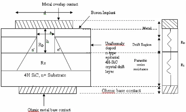
The common device structure of a 4H-SiC SBD is shown in Figure 1 and it’s equivalent circuit is also drawn in Figure 2. The SBD shown in Figure 1 consists of a block of n-type 4H-SiC crystal with a given height ‘h’. The metal contact at the top has a cross-sectional area ‘A’ and there is a base contact which may be formed using a metal or an alloy. Boron implant is made for edge termination on either side of the Schottky contact. An overlap exists between the top metallic contact of width ‘d’ and the contact length ‘a’. The current flow from the top contact is considered trapezoidal in shape spreading through the drift region by an angle ‘’ with the vertical at the corner edge of the boron implant beneath the contact. A standard value of =26O is taken for this model [13], which allows a
small spread of current from the top contact to uniformly flow into the n+-substrate below. The
equivalent circuit shown in Figure 2 of the SBD has Ron-sp which is the sum of the series Ron-sp of the
drift region (RD) and the parasitic series resistance (Rs) with uniform current flow. Beneath this region
is the n+-type heavily doped substrate region whose resistance may be considered to be zero.
Figure 1. The structure and regions of a 4H-SiC SBD Figure 2. Equivalent circuit of SBD shown in Figure 1
The equation to evaluate Ron-sp of the device can be given by [13] : '
'
2
ln[1 tan ] tan
on sp D d h
R
a
] tan 2 1 ln[
tan' '
a h a
where d = a for minimum overlap of contact metal considered and 1
D
NeND
(3)
where ND is the donor density in the n-type epitaxial layer.
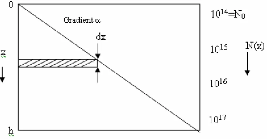
In the model proposed here for the 4H-SiC SBD, the epitaxial layer is not uniformly doped but is linearly graded with a gradient . Near the contact, the device has the lowest doping level (No),
which increases with the gradient to any desired doping level (N) at the substrate. This is shown in Figure 3. The equivalent circuit of the device is similar to Figure 2, with RD replaced by RD′ and the
new Rs ( Rs) being used. Rs has a lower value than Rs as the doping level is nearer to the substrate
than the contact at the top of the device. The doping level ND of the epitaxial layer has to be replaced
by the effective doping level Neff of the linearly graded drift layer.
Figure3. The 4H-SiC SBD with linearly graded drift Figure 4. The equivalent circuit region doping profile with gradient of the SBD shown in Figure 3
Formulation of Neff
Consider the cross section of the epitaxial layer of Figure 3 as shown in Figure 5. The resistance dR of a thin element of thickness dx at a distance x from the top of this device can be expressed as
'
1 dR=
( )
n
dx eN x A
Figure 5. Cross section of drift region of a 4H-SiC SBD with linearly graded profile and gradient where A is the cross-sectional area in the direction perpendicular to the figure. The total resistance R of this layer can be evaluated by writing N(x) = N0 + x and integrating within limits of x from 0
to h, where h is the height of the device. This gives
) (
' 1
0
0 N x
dx eA
R h
n
(5)Writing Z = N0 + x , then dZ = dx, which gives
0 00 1 ln 1
ln 1 1 0 0 N h eA N h N eA Z dZ eA R n n h N N n (6)
If the effective concentration of this layer is Neff, then R may also be written as
(7)
Comparing equations (6) and (7), Neff may be written as
) 1 ln( 0 N h h
Neff
(8)
The magnitude of Ron-sp of the linearly graded drift layer, i.e Ron-sp, can be obtained from equation (2)
with D replaced by D :
] tan 2 1 ln[
tan ' '
' ' a h a
Ronsp D (9)
where eff n D eN ' ' 1
(10)
with n being the value of mobility corresponding to doping level Neff of the drift region.
R = 1 h
A eNeff
Device height ‘h’
The height ‘h’ of the device has been set using a specific value of reverse bias voltage as the punch-through breakdown voltage. This is also set close to the avalanche breakdown voltage of the device using the condition pW = 1, the condition for avalanche breakdown, and has been set equal to W, the depletion width at punch-through. The p is the hole impact ionisation coefficient, wherein it is
assumed that hole in n-type wide depletion region in the drift layer started the ionisation process [14]. Calculation of power dissipation (PD)
The equation for power dissipation PD can be written as [9]:
on on sp L B
D J AR J AV
P 2
2
1 (11)
where Jon is the on-state current density, A is the device cross-sectional area for current flow, VB is the
reverse blocking voltage and JL is the leakage current density. For a 50% duty cycle, the magnitude of
JL in SiC devices is too small compared to that in silicon devices and hence the second term in
equation (11) can be neglected giving : )
( 2 1 2
sp on on
D J AR
P (12)
Evaluation of the on-state current density (Jon)
The current-voltage equation of the Schottky diode using thermionic emission theory has been given by Bethe [15] :
JF JS[exp(eVD/kT) 1] (13)
where JF is the on-state forward current density and VD is the voltage drop across the Schottky diode
and Js is the reverse leakage current density given by
Js = A T2 exp(-e B/kT) (14)
where A is the Richardson constant in amperes cm-2K2,
B is the barrier height in volt and T is the
device temperature in K.
The basic current–voltage equation for such a diode has been derived by Bhatnagar et al. [16]. The diode forward voltage drop (including drift layer) VF can be expressed as
VF = VD + JF Ron-sp (15)
Combining equations (13) through (15) and writing Jon for JF, the voltage VF may be expressed as
VF kTe ln(A TJon2) B J RF on sp
(16)
Values of Jon for different values of VF in the on state of the diode can be obtained by iteration
with a simple technique and C++ program [17]. Under forward bias and in the on state, the magnitude of VD and VF is small, and thus the effect of barrier height lowering, , has not been included in
The calculation of power dissipation has been performed, knowing ND, Neff, Ron-sp, Ron-sp and
the magnitude of Jon and VF, for both uniformly doped and linearly graded drift layers of the 4H-SiC
SBD’s.
Calculation of breakdown voltages
The punch-through breakdown voltage (VPBV) is determined at a high reverse bias voltage (VR)
for a uniformly doped semiconductor of 4H-SiC SBD and the depletion region width (W) at this voltage is set equal to the device height (h). The avalanche breakdown voltage is obtained using the condition p W = 1, to give the magnitude of p.The critical field (Ec) corresponding to this value of p
is obtained from [18]. The magnitude of the avalanche breakdown voltage (VAvBV) is then obtained
using the equations: VAvBV EcW
2 1
, for uniformly doped drift region of SBD, and (17)
'
3 2EW
VAvBV c , for linearly graded drift region of SBD (18)
The depletion region width in the two cases is calculated using the formula:
D R S
D R bi S
eN V eN
V V
W 2 ( ) 2 , for uniformly doped drift region of SBD, (19)
where Vbi is the built-in potential and Vbi<< VR, the applied reverse voltage which is equal to the
avalanche breakdown voltage, and
3
3 12 ( ) 12
e V e
V V
W S g R s R , for linearly graded drift region of SBD, (20)
where Vg is the gradient voltage and Vg<<VR, the applied reverse voltage which is equal to the
avalanche breakdown voltage. In the two equations, s denotes the permittivity of 4H-SiC and α in
equation (20) is the concentration gradient which is 1014 near the top of the device, and increases
linearly to 1015, 1016 ---, near the substrate over the device height (h).
The calculation of Ec for avalanche breakdown in a linearly graded profile is made using
equation [20]:
S
C e W
E
8
2
(21)
where W′ is the depletion region width at breakdown.
Calculations and related graphs
The device height ‘h’ is set equal to the maximum depletion region width ‘W’ corresponding to a breakdown voltage of 5 kV for the uniformly doped epitaxial layer with the lowest doping level of 1014 per cc using equation (19). This gives a value of 231µm for the device height ‘h’ taking ε
s = 9.7
magnitude of Ron-sp is calculated using equation (2) with angle ′ = 26 and Schottky contact of length
‘a’ equal to 100 µm. The contact width is equal to 78.5 µm. The device cross-sectional area ‘A’ is then 78.5 x 10⁻⁶ cm2. Specific values of the on-state current density (J
on) ranging from 100 to 1000 amps/
cm2 are used and the corresponding values of power dissipation (P
D) are calculated using equation
(12). This is repeated for doping levels of 1015, 1016 and 1017 per cc. The results are shown in Table
1(A).
Table 1(A). Calculation of power dissipation (PD) of 4H-SiC SBD with uniformly doped drift region
Nd = 1x 10¹⁴
atoms/cc
Nd = 1x 10¹⁵ atoms
/cc
Nd = 1x 10¹⁶
atoms/cc
Nd = 1x 10¹⁷
atoms/cc µn= 960 cm2 per
Vs
µn= 950 cm2 per Vs µn= 900 cm2 per Vs µn= 600 cm2 per
Vs Ron-sp =1.577
-cm2 Ron-sp =159.38x10
-3
-cm2 Ron-sp =16.82x10
-3
-cm2 Ron-sp =2.52 x 10 -3
-cm2
Current density (amps /cm2)
Jon
PD(1) Watts PD(2) Watts PD(3) Watts PD(4) Watts
100 0.6195 62.55x10⁻³ 6.601 x 10⁻³ 989.1 x 10⁻⁶
200 2.478 0.2502 26.40 x 10⁻³ 3.956 x 10⁻³
400 9.912 1.0008 0.1056 15.82 x 10⁻³
600 22.302 2.2518 0.2376 35.607 x 10⁻³
800 39.649 4.0032 0.4225 63.30 x 10⁻³
1000 61.95 6.255 0.660 98.91 x 10⁻³
In the case of linearly graded profiles, the device height ‘h’ is kept the same as in the case of the uniformly doped epitaxial layers (i.e 231 μm). The concentration gradients selected arbitrarily are 1014-1015, 1014-1016, 1014-1017 and 1014-1018 over the device height of 231µm. This gives the
concentration gradient ‘’ in each case. The effective carrier concentration ‘Neff’ for linearly graded
epitaxial layer is calculated using equation (8). The value of the average doping dependent carrier mobility (n′) for any specific concentration gradient is obtained from Roschkc and Schwierz [11].
Ron-sp is then calculated using equation (9), treating the medium doping level as equal to Neff. The
depletion region width ‘W’ for a reverse bias voltage of 5 kV is calculated using equation (20). The power dissipation for a given concentration gradient at the same current density levels in the case of the uniformly doped epitaxial layer device above is calculated using equation (12) with the same value of the device cross-sectional area ‘A’ and the corresponding values of Ron-sp. The results are shown in
Table 1(B).
Table 1(B). Calculation of power dissipation (PD) of 4H-SiC SBD with linearly graded drift region
Neff = 3.905 x 10 14
atoms/cc
Neff = 2.148 x10¹⁵
atoms/cc
Neff = 1.446 x10¹⁶
atoms/cc
Neff = 1.085 x10¹⁷
atoms/cc µn′= 960 cm2 per
Vs
µn′= 950 cm2 per
Vs
µn′= 900 cm2 per Vs µn′= 600 cm2 per Vs
Ron-sp =0.04038
-cm2 Ron-sp -cm2 =0.07418 Ron-sp = 11.63 x10 -3
-cm2 Ron-sp =2.325 x10
-3
-cm2
Current density (amps /cm2)
Jon
PD(1) Watts PD(2) Watts PD(3) Watts PD(4) Watts
100 0.15849 29.115e-3 4.565e-3 912.56e-6
200 0.63396 0.1164 18.260e-3 3.650e-3
400 2.5358 0.4658 73.042e-3 14.60e-3
600 5.7056 1.048 164.34e-3 32.85e-3
800 10.143 1.863 0.29217 58.40e-3
1000 15.849 2.9115 0.4565 91.25e-3
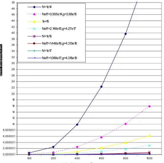
It is seen that linearly graded profiles give theoretically a much lower power dissipation (PD)
than do the uniformly doped profiles in 4H-SiC SBD’s. The percentage fall in power dissipation between two adjacent graphs of linearly doped and uniformly doped profiles in Figure 6 ranges from 7.74% to 74.4% for Jon of 1000 amps/cm2. This is shown in Figure 7.
The punch-through breakdown voltage (VPBV) is set at 5 kV for the case of uniformly doped
epitaxial layer with a doping level of 1014 per cc and a depletion region width ‘W’ of 231μm. The
condition for avalanche breakdown represented by pW = 1 gives the value of p. The magnitude of
the electrical field for avalanche breakdown (Ec) is obtained from Ayalew [18] from the plot of p
versus E for 4H-SiC. The value of VAvBV, the avalanche breakdown voltage, is then obtained from
equation (17). This is repeated for doping levels of 1015, 1016 and 1017 per cc, as shown in Table 2(A).
The punch-through breakdown voltage for the linearly graded epitaxial layer is obtained from the depletion region width ‘W’ at 5 kV for a given concentration gradient ‘’ of 3.88 x 1016cm-4. The
value of the critical field (Ec) for linearly graded profile is calculated using equation (21) and the value
of W obtained at 5 kV is treated as the depletion width for avalanche breakdown. The magnitude of VAvBV is then calculated using equation (18).This is repeated for other values of and the results are
0.000001 2.000001 4.000001 6.000001 8.000001 10 12 14 16 18 20 22 24 26 28 30 32 34 36 38 40 42 44 46 48 50
100 200 400 600 800 1000
current density(amps per cm2)
N=1e14
Neff=3.905e14,g=3.88e16 1e+15
Neff=2.148e15,g=4.27e17
N=1e16
Neff=1.446e16,g=4.313e18 N=1e17
Neff=1.088e17,g=4.316e19
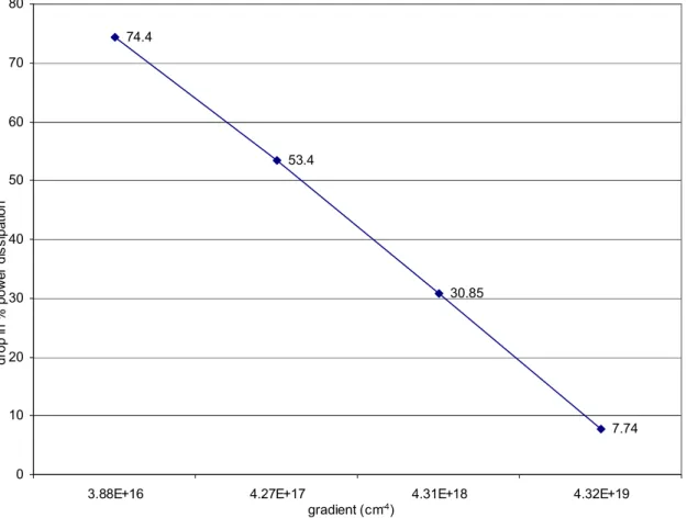
Figure 7. Percentage drop in power dissipation versus concentration gradient in 4H-SiC SBD compared to SBD with uniformly doped drift region
Table 2(A). Breakdown voltages of 4H-SiC SBD for uniformly doped epitaxial layer (Device height = h = W = 231 μm)
Doping level (ND per
cc)
W (m) p (cm-1) Ec (V per cm)
x 106 VAvBV (kV) VPBV (kV)
1014 227 44.05 1.33 14.94 5
1015 71.78 139.31 1.66 5.95 5
1016 22.7 440.05 1.82 2.06 5
1017 7.17 1394.7 2.12 0.7575 5
74.4
53.4
30.85
7.74
0 10 20 30 40 50 60 70 80
3.88E+16 4.27E+17 4.31E+18 4.32E+19
gradient (cm-4)
dr
op
in
%
p
ow
er
d
is
si
pa
tio
Table 2(B). Breakdown voltages of 4H-SiC SBD for linearly graded epitaxial layer (Device height = h = W = 231 μm)
Gradient (cm-4)
W (µm)
S
C e W
E
8
2
' VAvBV (kV) VPBV (kV)
3.88 x 10¹⁶ 201.07 3.72 x 10⁵ 4.986 5
4.27 x 10¹⁷ 90.3 8.25 x 10⁵ 4.966 5
4.31 x 10¹⁸ 41.8 2.86 x 10⁶ 4.966 5
4.31 x 10¹⁹ 19.4 3.84 x 10⁶ 4.966 5
4.4 x 10¹⁹ 22.7 5.26 x 10⁶ 7.960 8
Discussion and Conclusions
The curves shown in Figure 6 show that the linearly graded epitaxial drift region of 4H-SiC SBDs have consistently lower power dissipation than the uniformly doped epitaxial layer devices. A tally of such an effect can be verified by comparing the power dissipation of the devices when evaluated at a current density of 1000 amps/cm2. The comparison between the curve for the uniformly
doped epitaxial layer device with a doping level of 1014 per cc and that for the linearly graded profile
with a gradient of 3.88 x 1016 cm-4 at Neff of 3.905 x 10¹⁴ shows that there is a 74.4% drop in power
dissipation. When the drop in power dissipation is evaluated at other current density levels, it is found that the drop in per cent power dissipation remains at the same level. This is, however, not so for other sets of curves, where this type of tally shows a constant decline in per cent power dissipation for a given Neff compared to nearly similar levels of doping in the uniformly doped profiles. In other words,
compared to the uniformly doped epitaxial layers, the linearly graded profiles show a significantly lower power dissipation. Figure 7 shows this in a different perspective where the percentage fall in power dissipation is found to increase with a decrease in concentration gradient from 74.4% at a gradient of 3.88 x 1016 cm-4 to 7.74% at a gradient of 4.316 x 1019 cm-4
Calculation of breakdown voltages shown in Table 2(A) shows that for uniformly doped epitaxial layer devices doped to a level of 1015 per cc, the punch-through and avalanche breakdown
voltages are almost equal to 5 kV. Linearly graded epitaxial layer devices show a similar avalanche breakdown at 7.96 kV for a gradient of 4.4 x 1019 cm-4 for which the punch-through breakdown voltage is 8 kV. This device can therefore have a breakdown voltage of 7.96 kV which is almost equal to the punch-through breakdown voltage of 8 kV.
An analysis of the results shown in Tables 2(A) and 2(B) shows that the critical field ‘Ec’
increases with doping level in the case of uniformly doped epitaxial layer devices while it does with gradient in the case of linearly graded epitaxial layer devices. However, the magnitude of Ec in the
former case is somewhat higher than that in the latter case. The depletion region width in devices with uniformly doped profiles is normally larger than that with linearly graded ones.
voltage. Lastly, the device height ‘h’ of 231µm used in this work may be difficult to grow in 4H-SiC using epitaxial technology. However, wafers with better crystalline perfection may be selected for making these devices.
References
1. T. P. Chow, “SiC and GaN high-voltage power switching devices”, in: Silicon Carbide and Related Materials 1999, Materials Science Forum (Ed. C. H. Carter, Jr, R. P. Devaty and G. S. Rohrer), Vols. 338-342, Trans. Tech. Publications Ltd., Switzerland, 2000, pp. 1155-1160.
2. R. Rupp, M. Treu, A. Mauder, E. Griebl, W. Werner, W. Bartsch and D. Stephani, “Performance and reliability issues of SiC-Schottky diodes”, in: Silicon Carbide and Related Materials 1999, Materials Science Forum (Ed. C. H. Carter, Jr, R. P. Devaty, and G. S. Rohrer) Vols. 338-342, Trans. Tech. Publications Ltd., Switzerland, 1999, 1167-1170.
3. M. S. Mazzola and S. E. Saddow, “High voltage SiC power device field terminations”, 2nd International All Electric Combat Vehicle Conference, 8-12 June, 1997, Dearborn, MI, USA , pp. 1-6.
4. J. B. Dufrene, G. Carter, J. B.Casady, I. Sankin, D. C. Sheridan, W. Draper and M. Mazzola, “High voltage silicon carbide diode development”, 16th Annual IEEE Conference on Applied Power Electronics, 4-8 March, 2001, Anaheim, CA, USA, pp.1253-1257.
5. W. J. Schaffer, G. H. Negley, K. G. Irvine and J. W. Palmour, “Conductivity anisotropy in epitaxial 6H and 4H SiC in diamond, SiC and nitride wide band gap semiconductors”, Mater. Res. Soc. Proc., 1994, 339, 595-600.
6. D. Alok, B. J. Baliga and P. K. Mclarty, “A simple edge termination for silicon carbide devices with nearly ideal breakdown voltage”, IEEE Trans. Electron Devices, 1993, 15, 394-395.
7. R. Raghunathan, D. Alok and B. J. Baliga, “High voltage 4H-SiC Schottky barrier diodes”, IEEE Trans. Electron Devices, 1995, 16, 226-227.
8. A. Itoh, T. Kimoto and H. Matsunami, “High performance high-voltage 4H-SiC Schottky barrier diodes”, IEEE Electron Device Lett., 1995, 16, 280-282.
9. M. Bhatnagar and B. J. Baliga, “Comparison of 6H-SiC, 3C-SiC and Si for power devices”, IEEE Trans. Electron Devices, 1993, 40, 645-655.
10. W. J. Schaffer, G. H. Negley, K. G. Irvine and J. W. Palmour, “Conductivity anisotropy in epitaxial 6H and 4H-SiC”, Mater. Res. Soc. Symp. Proc., 1994, 339, 595-600.
11. M. Roschke and F. Schwierz, “Electron mobility models for 4H, 6H and 3C SiC”, IEEE Trans. Electron Devices, 2001, 48, 1442-1447.
12. I. A Khan and J. A. Cooper, Jr., “Measurement of high-field electron transport in silicon carbide”, IEEE Trans. Electron Devices, 2000, 47, 269-273.
13. B. J. Baliga, “Modern Power Devices”, Wiley, New York, 1997, Ch. 4.
15. H. A. Bethe, “Theory of the boundary layer of crystal rectifiers”, MIT Radiation Laboratory Report No. 43-12, 1942, obtainable from Publications Board, Department of Commerce, Washington D.C.
16. M. Bhatnagar, P. K. McLarty and B. J. Baliga, “Silicon carbide high voltage (400V) Schottky barrier diodes”, IEEE Electron Device Lett., 1992,13, 501-503.
17. R. Talwar and A. K.Chatterjee, “A method to calculate the voltage-current characteristics of 4H SiC Schottky barrier diode”, Maejo Int. J. Sci. Technol., 2009, 3, 287-294.
18. Dissertation Tesfaye Ayalew, http://www.iue.tuwien.ac.at/phd/ayalew/node74.html
19. S. M. Sze , “Physics of Semiconductor Devices”, 3rd Edn., John Wiley and Sons, New York, 1999,
p. 81.