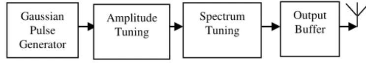
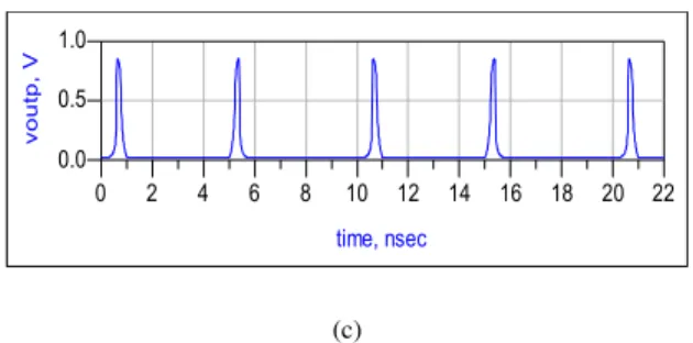
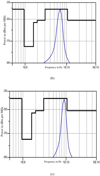
3.51pJ pulse 1.2V CMOS IR-UWB Transmitter
Texto
Imagem


Documentos relacionados
Convict that the water exercises has for a long time left of being restricted activity to a special group of individuals, and feeling the need of scientifi c background and
Nesse ponto, pretende-se com o presente artigo discutir a introdução do WhatsApp como ferramenta destinada ao profissional da saúde para estreitamente da relação com o seu paciente
O mesmo se pode concluir dos restantes três fatores mencionados acima (Confiança, Qualidade e Preço) que apresentaram resultados semelhantes aos da Satisfação, reafirmando a sua
Entre os assuntos que podiam provocar avaliações consideradas “erradas” pelos integralistas estavam: a relação entre o integralismo e o fascismo; a questão do
Cada área da cidade deve ter uma parcela de área verde e superfície de água para criar no seu entorno condições confortáveis de ambiência higrotérmica e de qualidade de ar
Conversaciones sobre el comunismo anárquico Autor: Errico Malatesta Tradutor: Editor: Biblioteca del Grupo Germinal Preço: Tiragem: Custo da edição: Páginas: Formato: Idioma:
Enquanto o CS/ONU não for reformado e tiver mais capacidade de decisão para resolver crises e conflitos mundiais, onde se põem graves problemas de violência (de origem
O Defensor Público-Chefe Federal no Estado de Santa Catarina VICTOR HUGO BRASIL, no uso de suas atribuições institucionais e legais, com fundamento na Lei Complementar nº 80/94 e na
