Alexandre M. De Oliveira
a, Héctor D. O. Ascamaa, Roberto K. Hiramatsua, Sérgio T. Kofujia,a
Departmento de Engenharia de Sistemas Eletrônicos, Escola Politécnica, Universidade de São Paulo, Av. Prof. Luciano Gualberto, travessa 3, 158, CEP 05424-970, São Paulo, SP, Brasil.
e-mail:{amanicoba, hector, kenji, kofuji}@pad.lsi.usp.br; Marcelo B. Perotonib,
b
Universidade Federal do ABC, Avenida dos Estados, 5001, CEP 09210-170, Santo André, SP, Brasil. e-mail:[email protected]
João F. Justoa e-mail:[email protected]
Abstract— This work presents a new Ultra Wide Band (UWB) beamforming fifth-order derivative Gaussian pulse transmitter with dual small Vivaldi antennas for remote acquisition of vital signals in impulse radar applications. The system consists of a programmable delay circuit (PDC or τ), a UWB pulse generator (PG) circuit and an array of two Vivaldi planar antennas. The circuits is designed using the 0.18μm CMOS IBM process. Spice simulations show the pulse generation with 90mVpp amplitude and 300ps width. The average power consumption is 120µW per pulse, using a 2V power supply at a pulse repetition rate (PRR) of 100MHz. Full tridimensional electromagnetic simulations, using CST MWS, show the main lobe radiation with a gain of 5.5dB, and a beam steering between 20º and -17.5º for azimuthal (θ) angles at the center frequency of 7.5GHz.
Index Terms— Health monitoring; respiration rate; beamforming; phased
array; vital signals; heartbeat signals.
I. INTRODUCTION
Considerable effort has been focused on the generation and transmission of UWB pulses, which can be used
in a wide range of applications, such as in the remote acquisition of heartbeat signals of workers in an industrial
plant, the measurement of respiration rate of soldiers in a military vehicle, or to track victims in landslide rubble
[1-3]. This system consists of a transmitter, described in this work, and a receiver to perform telemetry for
estimating the vital signs through detection of heart and lungs.
In order to acquire those signals, it is required to have a high precision system that can dynamically capture
the signals of each individual on its fixed position, since this analysis in motion can cause significant changes in
the shape of the UWB waveform [4].
If the spectral power of the UWB pulses is spread along an ultra-wide frequency range, the interference with
other communication systems, such as phones, GPS systems, Bluetooth, and W-LAN IEEE 802.11, could be
minimized [5]. A critical point is that reflections from the environment need to be minimized, in order to
preserve the pulse shape and facilitate the detection process. Therefore, it is essential to use a radar system
equipped with high-gain directional antennas [4]. The proposed arrangement, based on the model discussed in
ref. [1], contains a timed-array transmitter system which is equipped with an antenna array that allows beam
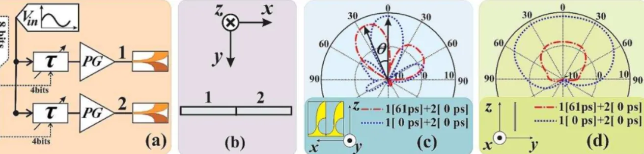
steering (Fig. 1). In the figures 1(c) and 1(d), two polar gain plots are shown, where each one corresponds to a
A CMOS UWB Transmitter with Vivaldi Array
This paper is organized as follows: Sec II presents the transmitter circuit and antenna array architecture and
design; the integrated system post-layout Spice simulations with MicroWind 3[6] combined with LTSpice 4[7]
for layout and schematic, where effects of crosstalk coupling vertical and horizontal, input noise and parameters
variation by Monte Carlo were considered during the Spice simulations. Section III presents the results of
electromagnetic propagation simulation in CST MW 2011[8], together with the results of Spice simulations,
while Section IV presents the conclusions.
Fig. 1 - UWB Beamforming Transmitter. (a) A general structure of beamforming; (b) Back view of the two antenna array; alongside with the axes orientation; (c) array gain pattern in the azimuth plane and antenna array view from the top; (d) array
gain pattern in the elevation plane and lateral antenna array view.
II. TIMED-ARRAYTRANSMITTERCIRCUITANDANTENNAARRAYWITH BEAMFORMINGCAPABILITY
Radar systems based on timed or phased antenna have several advantages in comparison to
mechanically scanned systems, since with electronic configurations the beam steering can be achieved
rapidly without the use of complicated mechanical systems [9], e.g. when the antennas are excited
with a delay time of 61ps and 0ps for channels 1 and 2 respectively, the same channels will vary the
azimuthal angle (θ), as seen in Fig. 1(c), and elevation angle (φ) as seen in Fig. 1(d). Each block of
the transmitter is explained, including the antenna array in the next sections.
A. Programmable delay array – PDC
The proposed PDC is shown in Fig. 2(a). The circuit consists of two independent channels (such
that each antenna can be independently fed), further details shown in Fig. 2(b), and each one is
formed by two buffers formed by two static inverters (Fig. 2(e)), connected in series with a digital
variable capacitor (Fig. 2(c)), between the signal line and Vss.
Fig. 2 - General PDC array structure: (a) PDC array; (b) PDC Unit; (c) Digital Variable Capacitor Circuit; (d) MOS dimension table of the PDC Unit; (e) Buffer Circuit.
between the two internal buffers, therefore providing a controlled delay.
B. The 5th derivative Gaussian pulse generator
UWB radars can be used as a tool for analysis of human vital signs in a noninvasive form. They are
not influenced by clothing or other covers and can be used at range of several meters [10].
The first consideration before designing a UWB pulse generator is to select the type of pulse that
meets certain conditions [11]. According to refs. [11, 12], the Gaussian pulse can be expressed as,
√ (
)
(1)
where is the time variance and A is the pulse amplitude. The Gaussian pulse is a natural candidate
for a UWB pulse because it has a wide bandwidth and no side lobes, albeit it contains a DC and
lower frequency components, which cannot be transmitted by the antennas considered here.
The fifth-order derivative Gaussian pulse is one of the best choices, for noninvasively health
monitoring, because it fully complies with the FCC mask for indoor applications [11-13] and there is
no DC energy (zero frequency). As a result, the fifth-order derivative Gaussian was chosen for the
proposed pulse generator development. Therefore, the proposed pulse generator is expressed as
√
√
√
( )
(2)
Fig. 3 – The proposed UWB 5th derivative Gaussian pulse generator: (a) General structure of the proposed pulse generator; (b) Simplified time diagram; (c) Pulse Generator proposed for [11]; (d) AND gate formed by a pseudo n-MOS NAND gate
and a static inverter; (e) Static inverter circuit; (f) Three Inverter Delay Circuit.
The novel system architecture is illustrated in Fig. 3(a). It consists of two identical static inverters
connected in series. They transform the arbitrary input signal Vininto a square waveform Vtrigger (Vtg).
Next, there is a triangular pulse generator [14], responsible for the generation of a triangular pulse that
is inverted by the static inverter (Va). This inverted triangular pulse is later spread and inverted by the
delay line (Vb, Vc, and Vd), each time the wave excites the pulse shape transistors (M9p, M8n, M7p,
and M10n). The current that passes through the C capacitor blocks out the DC component, and also
generates the Vout signal that is shaped according to the 5th derivative of the Gaussian pulse, as
illustrated in Fig. 3(b).
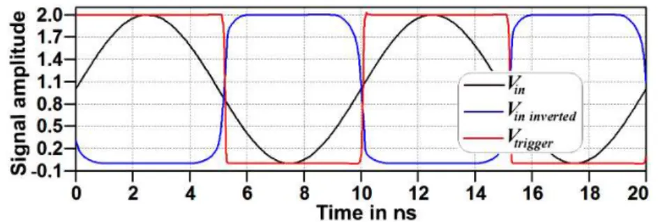
1) Square-wave rectifier
This subsystem consists of two identical static inverters used to rectify time-varying waveforms
such as square waves, following the proposed pulse generator presented in [15]. The inverter
architecture is illustrated in Fig. 3(e), which consists of the pMOS (M11p with w=4µm and l=0.2µm)
and the nMOS (M12n with w=2µm and l=0.2µm) transistors, operating as switches. When the input
signal has a low level (Vss), the nMOS gate is reversely biased while the pMOS gate is directly
biased, therefore generating a high level (Vdd) at its output. Conversely, a high level signal is applied
in the input generates a low level (Vss) on the output.
Because the average time response from Monte Carlos simulations of the proposed inverter lies in
the range of 40ps (more than seven times faster compared to the transition from a sine wave of the
same frequency), the connection of two inverters in series shapes the input time-varying signal into a
square wave.
The Fig. 4 shows the waveforms Vin, and Vin inverted Vtg as a result of the Spice simulation [6, 7].
Fig. 4 - Waveform of the input signal (Vin) that passes through the first static inverter (Vin inverted) and (Vtrigger), after it passes
through the second static inverter.
The same inverter is used in the output of the triangular pulse generator.
2) Triangle pulse generator
The Triangle pulse generator used in this work is based in the developments of [14] and is the core
of the 5th derivative Gaussian proposed pulse generator. Fig. 3(c) shows the triangle pulse generator,
which is originally used as the single pulse generator [14], and was developed around a simple
feedback network and an AND gate.
Fig. 5 - Waveform of the rectified input signal (Vtrigger), the middle signal of triangle pulse generator (Vx) and the pulse
generated (Vpulse).
flow is shown in Fig. 5. When Vtrigger is held at a low level (Vss), the AND gate (Fig. 3 (d)) output is
also at low level, thus the nMOS transistor M14n (with w=1µm and l=0.2µm) is off. The parasitic
capacitor Cx is then charged to Vdd by the pMOS transistor M13p (with w=4µm and l=0.2µm). At the
moment that the Vtrigger signal reaches the high level (Vdd), M13p is immediately turned off and the
AND gate output reaches a high level after a short gate delay AND, therefore M14n is turned on to
discharge the capacitor Cx. When the signal Vx is changed to a level below the threshold voltage of the
AND gate VTH AND, the AND gate output changes to a low level again after T, thereby a triangular
pulse (Vpulse) is produced. Considering that the switch-on impedance of M14n is RON, it can be
estimated that:
⁄
(3)
when Vx(t) is changed to a level below VTH AND, the AND gate output is at low level and turns M14n
off after the gate delay ( AND). The discharging time is:
⁄
(4)
and the triangle pulse width ( tp) is equal to the sum of the AND time with (4):
⁄
(5)
Therefore, we conclude that the pulse width varies with the following characteristics: AND gate delay time ( AND);
Parasitic capacitance of the interconnection x (Cx);
M14n switch-on impedance (RON);
It should be stressed that RON is not constant, since Vpulse is variable. Further circuit simulations may
be required to compute more accurate pulse widths.
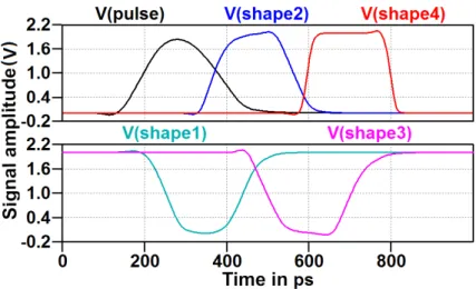
3) Delay circuit
The delay unit is formed by three sets of identical static inverters. In Fig. 3(f), each implemented
inverter consists of the nMOS and pMOS transistors, for the first inverter they are M23n (with
w=2µm and l=0.2µm) and M20p (with w=4µm and l=0.2µm), respectively.
The delay time depends on the transistor channel dimensions; on the parasitic capacitances and the
number of inverters in the delay line. This particular setting for the delay circuit was chosen due to its
simplicity and compact topology. The outputs of the Vpulse, Vshape1 (Va) and the three delay elements
are Vshape2 (Vb), Vshape3 (Vc), and Vshape4 (Vd), respectively, and they have an average width time of
190ps. Fig. 6 shows Vpulse and the other triangle waves that excite the transistors forming the pulse
Fig. 6 - Waveform of the triangles pulses starting with the input Vpulsesignal, followed by Vshape1 (Va), Vshape2 (Vb), Vshape3
(Vc), and Vshape4 (Vd).
4) Pulse shaping stage
The development of the pulse shaping stage presented in this paper is based on [1, 11, 14, 15]. The
pulse shaping stage implemented two charge-pumps, each consisting of two transistors, a pMOS and a
nMOS, M9p (with w=2µm and l=0.2µm), M8n (with w=6µm and l=0.2µm), M7p (with w=6µm and
l=0.2µm), and M10n (with w=2µm and l=0.2µm), as shown in Fig. 3(a). The charge-pump output
currents are controlled and combined successively by these transistors; as a result, a fifth derivative
Gaussian pulse is generated, illustrated in Fig. 3(b) and its waveform is shown in Fig. 8(a). The output
pulse amplitude Vout is controlled by the charge-pumps output transistors. The transistor sizes are
chosen based on the required amplification level to shape the output UWB waveform [10,14].
5) Pulse generator simulation results
The simulation of the proposed UWB pulse generator in post-layout Spice model shows that the
circuit can be robustly operated, in other words, showing the 5th Gaussian pulse waveform at Vout
unchanged with 20% variation of the parameters in Monte Carlo simulations. In order to confirm this,
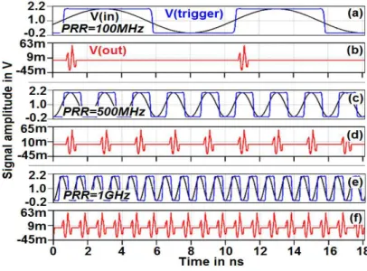
the circuit was simulated in several PRR’s up to the GHz band range. The results from 100MHz up to
1.0GHz are shown in Fig. 7, where Fig. 7(a) shows the input sinusoidal signal waveform (Vin) and its
rectified signal (Vtrigger) at 100MHz. Fig. 7(b) presents the waveform of the pulse simulated (Vout) with
a PRR of 100MHz, Fig. 7(c) shows the waveform Vin and Vtrigger at 500MHz. Fig. 7(d) shows the
waveform Vout with a PRR of 500MHz, in the GHZ range finally, the Fig. 7(e) shows the wave form
Vin and Vtriggerat 1.0GHz and Fig. 7(f) show the waveforms of Voutpulse train at PRR of 1.0GHz.
The simulation results showed that the fifth-order derivative Gaussian pulse is similar to the
theoretical pulse calculated , as shown in Fig. 8(a). The amplitude of the simulated pulse is 90mVpp
Fig. 7. Pulse simulated with different PRR: (a) Vin and Vtriggerat 100MHz. (b) Voutwith PRR at 100MHz. (c) Vin and Vtriggerat
500MHz. (d) Voutwith PRR at 500MHz. (e) Vin and Vtrigger at 1.0GHz. And (f) Voutwith PRR at 1.0GHz.
Fig. 8. (a) Simulated versus theoretical 5th Derivative Gaussian Pulse, (b) Spice Power Spectral Density of output pulse.
Figure 8(b) shows that the pulse spectral density is in good agreement with the FCC mask for UWB
applications. The simulated power spectral density (PSD) of the proposed pulse is indicated in solid
line, whereas the three-dot-dashed line shows the theoretical fifth-order Gaussian pulse PSD,
alongside with the FCC mask for indoor UWB applications.
Table I compares this design with others reported in the literature. Comparison with [16] shows that
the power consumption of this design is lower, as a result of the lower signal duration and smaller
TABLE I. PERFORMANCE AND COMPARISON OF UWB TRANSMITTERS
Parameters This work [16] [15]
Gaussian pulse derivative order 5th 5th 5th
Technology 0.18µm 0.18µm 0.50µm
Power supply 2V 1.8V 1.8V
PRR 100MHz 100MHz 20MHz
Pulse duration 300ps 420ps 2400ps
Pulse amplitude 90mVpp 51mVpp 160mVpp
Power consumption per pulse. 120µW 3.6mW 1.159mW
Circuit area (without pads) 23x46µm² 240x560µm² --
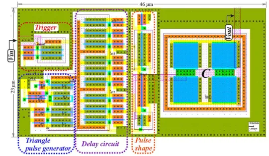
6) Proposed Layout
Figure 9 shows the layout of the proposed UWB pulse generator circuit without the pads, where it is
shown the areas of the input signal trigger, the triangle pulse generator, the delay circuit, the pulse
shaping circuit, and the capacitor C. Guard rings are used to minimize latch-up effects and
interference between adjacent circuits. The complete pulse generator circuit occupies an area of 23x46μm², whereas the total array transmitter occupies only about 80x96μm². The capacitor occupies a large area of the chip (nominally 40%).
Fig 9. Layout of one pulse generator of the array UWB without pads.
B. Vivaldi antenna array
It is proposed an array of two antipodal Vivaldi antennas for the beamforming. The Vivaldi
antennas belong to the class of aperiodic, continuously scaled, exponential curved antennas. The
characteristics that make it suitable for UWB applications are that the Vivaldi antenna has
theoretically constant beamwidth at unlimited operating frequency range [17, 18, 19]. This planar
antenna is basically formed by a Microstrip Transition Line (MTL) and an exponential slot line
1) Microstrip Trasition line
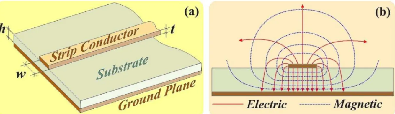
A MTL is defined as a transition line formed of a strip conductor and a ground plane isolated by a
structural subtract (Fig. 10), usually with high dielectric constant (ε > 2), separating the ground plane
of the microstrip line, both made by a thin metallic film, which is generally copper [14-21]. Since
field lines are not totally contained in the substrate, the propagating mode in the strip line is not purely
transverse electromagnetic (TEM), in this case is quasi-TEM [14-21].
Fig. 10. Microstrip Transition line where h and t are the substrate and strip conductor thickness respectively, and w is the
strip conductor width (a). A quasi-TEM analysis is represented (b) [20].
According to ref. [20], when the proportional relationship between w and h is greater than 1, the
transition line has a characteristic impedance and an effective dielectric constant given by
√
⁄
⁄ ⁄
(6)
where
⁄
⁄
(7)
In order to ensure a match with cables and circuits, that use a reference impedance of 50 Ω, the
following parameters were used: the substrate chosen was the FR-4, whose dielectric constant is 4.3
and loss tangent of 0.025, the thickness (h) was chosen as 1 mm. It was used the analytical impedance
calculation routine of the CST [8] to estimate the impedance of different widths (w). Therefore, the
value of w = 1.815 with a εeff = 3.25 was obtained.
2) Exponential Slot Line Radiator
After obtaining the impedance matching between the circuit and the MTL, the goal is now to
perform a smooth transition between the MTL and the signal propagation medium (air). For this
transition, we considered a slot line radiator in the exponential tapered shape, since this ensures a
relatively wide impedance bandwidth [17-19].
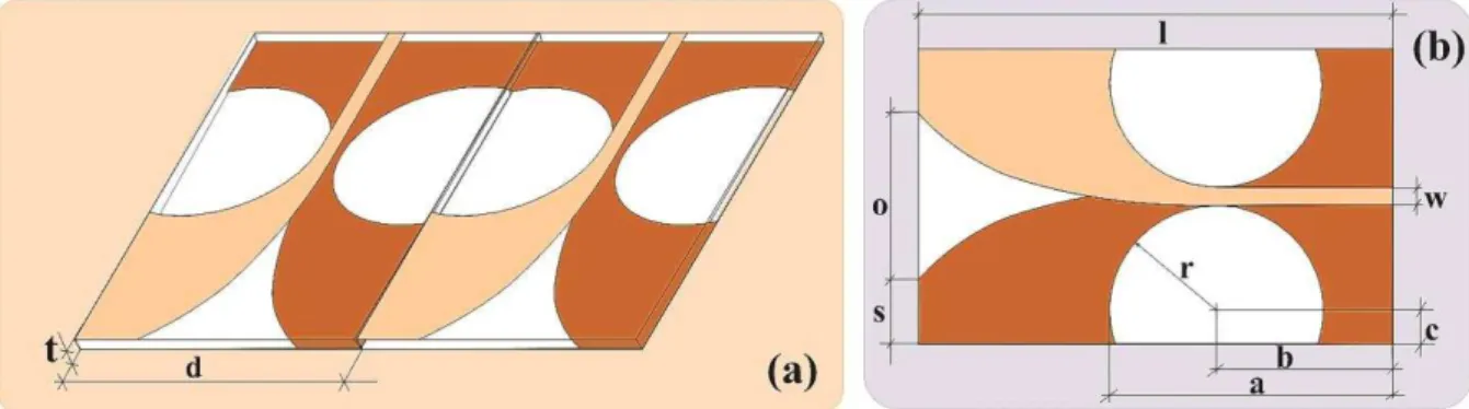
The opening function of the slot line radiator is shown in equations (8), (9) and (10), and is defined
by the opening rate (R=0,105) and the points P1(x1,y1) and P2(x2,y2), as depicted in Fig. 11,
where
(9)
And
(10)
Fig. 11. Designed antipodal Vivaldi antenna, highlighting the Cartesian plane and the exponential shape of its opening.
3) Proposed Vivaldi antenna array
An array of two antipodal Vivaldi antennas for beamforming is proposed. The design parameters of
dual-polarized array and Vivaldi antenna are shown in Fig. 12, and its respective dimensions in Table II.
Fig. 12. (a) Key design parameters of array; (b) Key design parameters of the individual notch Vivaldi antenna.
TABLE II. DIMENSIONS OF THE ANTENNAS.
50Ω microstrip line w b Units in mm.
1,815 21,20
Antenna dimensions l o s r c a
58,40 22,66 7,89 13,40 1,90 34,60
Figure13 shows the simulated scattering parameter S11 of the antenna. It can be seen that after
6GHz the return loss is less than 10 dB.
III. SIMULATIONRESULTS
The simulation of the complete Pulse Beamforming Transmitter in post-layout Spice model shows a
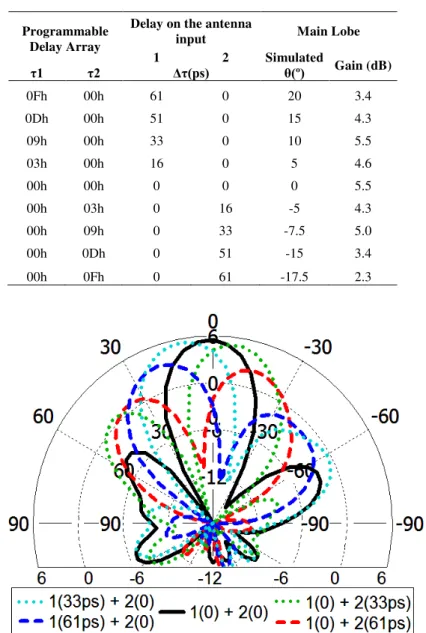
pulse amplitude of 90mVpp and 300ps of pulse width, as well as a main lobe with gain of 5.5dB, (32º x 132º angular width). The beam can be steered between 20º and -17.5º relative to the θ angle Fig. 1(c), obtained through programmable delays ranging from 0 to 61ps, using the proposed PDC.
Table III and Fig. 14 show some possibilities for beamforming alongside with the required
configuration parameters. Here, the first to second column are the PDC control words, in hexadecimal
base; the third and fourth column contain the corresponding time delays; and, finally, fifth and sixth
columns are of the beam radiated steering and gain results.
TABLE III. POSSIBLE CONTROL SETS AND RESULTS AT 7.5GHZ.
Programmable Delay Array
Delay on the antenna
input Main Lobe
1 2 Simulated
Gain (dB)
τ1 τ2 Δτ(ps) θ(º)
0Fh 00h 61 0 20 3.4
0Dh 00h 51 0 15 4.3
09h 00h 33 0 10 5.5
03h 00h 16 0 5 4.6
00h 00h 0 0 0 5.5
00h 03h 0 16 -5 4.3
00h 09h 0 33 -7.5 5.0
00h 0Dh 0 51 -15 3.4
00h 0Fh 0 61 -17.5 2.3
Fig. 14. Radiation pattern of the Fairfield (array) Gain (dB) x Theta (degrees) for some configuration parameters possibilities.
IV. CONCLUSION
of CMOS technology, as well as an antenna array design integrated with Spice and CST 2011 MW
were presented. The simulation results showed a controllable beam steering between 20º and -17.5º for θ angle with an average gain of 5.5dB, 32º x 132º angular width. This control was achieved using a PDC array circuit that can generate delays digitally controlled from 0 to 61ps. The pulses obtained
present 90mVpp amplitude and 300ps of pulse duration and a power consumption around 120µW per
pulse using 2V power supply at PPR of 100MHz.
REFERENCES
[1] A. M. de Oliveira, H. D. O. Ascama, W. V. Noije, L. C. Moreira, S. T. Kofuji, “A CMOS UWB Pulse Beamforming Transmitter with Vivaldi Array Antenna for Vital Signals Monitoring Applictions” Proceedings of 3rd IEEE Latin American Symposium on Circuits and Systems (LASCAS´12), EUA : IEEEXplore, 2012.
[2] D. Zito, D. Pepe, M. Mincica, F. Zito, A. Tognetti, A. Lanata, D. de Rossi, "SoC CMOS UWB Pulse Radar Sensor for Contactless Respiratory Rate Monitoring". IEEE Transactions on Biomedical Circuits and Systems. vol. 5. pp. 503-510. Dec. 2011
[3] M. Baldi, F. Chiaraluce, B. Zanaj, M. Moretti, “Analysis and simulation of algorithms for vital signs detection using UWB radars”. Proceedings of 2011 IEEE International Conference on Ultra-Wideband (ICUWB). ISBN: 978-1-4577-1763-5. p. 341 – 345. 2011.
[4] E. Sharifahmadian. et al. " Adaptive Signal Processing Algorithm for Remote Detection of Heart Rate (HR) Using Ultra-Wideband Waveforms based on Principal Component Analysis". In: 31st Annual International Conference of the IEEE EMBS, 2009, Minneapolis - Minnesota, USA.
[5] J. S. Araújo, R. M. S. de Oliveira, C. L. S. S. Sobrinho. “Novel Technique for Locating na Intruder in 3D Environments by Using a Cooperative System of Multistatic Radars” Journal of Microwaves, Optoelectronics and Electromagnetic Applications. vol. 10, no. 2 . p. 308 – 322. December 2011.
[6] Microwind v.3, Dr. Etienne Sicard, Toulouse, France.
[7] Linear Technology Spice (LTSpice) v.4. Linear Technology, Milpitas, CA.
[8] Computer Simulation Technology (CST) Microwave Studio (MWS) v.2011, CST of America, Inc., Wellesley MA.
[9] N.N.M. Khanh, M. Sasaki, K. Asada. “A CMOS Pulse Beamforming Transmitter Design with an On-chip Antenna Array for Millimeter Wave Imaging Applications”, 5th FutureTech 2010, Busan, Korea, pp. 1-6, May 2010.
[10] E. M. Staderini "UWB Radars in Medicine". IEEE Aerospace and Electronic Systems Magazine, vol 17, pp. 13-18, Aug. 2002.
[11] T. A. Phan, V. Krizhanovskii, S. K. Han, S. G. Lee.“4.7pJ/pulse 7th Derivative Gaussian Pulse Generator for Impulse Radio”, AUTO-ID Labs at MIT, 2008.
[12] H. Sheng, P. Orlik, A. M. Haimovich, L.J. Cimini, J. Zhang; “On the spectral and power requirements for ultra -wideband transmission” Proceedings of IEEE International Conference on Communications (ICC´03), ISBN: 0 -7803-7802-4, 2003., p.738-742.
[13] FCC - Federal Communication Commission, Revision of Part 15 of the Commission’s Rules Regarding Ultra -Wideband Transmission Systems, adopted Feb. 2002, released Apr. 2002.
[15] H. Kim, Y. Joo. "Fifth-derivative Gaussian pulse generator for UWB system". IEEE Radio Frequency integrated circuits (RFIC) Symposium, 2005. ISBN: 0-7803-8983-2. pp. 671-674. Aug. 2005.
[16] H. Xie, X. Wang, A. Wang, B. Zhao, Y. Zhou, B. Qin, H. Chen, Z. Wang. "A varying pulse width 5th-derivative gaussian pulse generator for UWB transceivers in CMOS" Proceedings of IEEE Radio and Wireless Symposium, 2008. ISBN: 978-1-4244-1463-5, 2008., p.171 - 174.
[17] Y. Yang, Y. Wang, A. E. Fathy. “Design Of Compact Vivaldi Antenna Arrays For UWB See Through Wall Applications”. Progress in Electromagnetics Research, PIER 82, p.401-418, 2008.
[18] M. C. Greenberg, L. Virga, C. L. Hammond, “Performance characteristics of the dual exponentially tapered slot antenna for wireless communication application,” IEEE Trans. On Vehicular Technology, vol. 52, p.305-310, Mar. 2003.
[19] A. Mehdipour, K. Mohammadpour-Aghdam, R. Faraji-Dana. “Complete Dispersion Analysis of Vivaldi Antenna For Ultra Wideband Applications” Progress In Electromagnetics Research, PIER, vol. 77, p.85-96, 2007.
[20] I. J. Bahl, D. K. Trivedi. “A designer's guide to microstrip line”. Microwaves, 1977; 16: 174–182.