Radial breathing mode resonance Raman cross-section analysis in single-walled carbon
nanotubes
Pedro Barros Cotta Pesce
Radial breathing mode resonance Raman cross-section analysis
in single-walled carbon nanotubes
Pedro Barros Cotta Pesce
Orientador: Prof. Ado J´orio de Vasconcelos
Disserta¸c˜ao apresentada `a Universidade Federal de Minas Gerais como requisito parcial para a obten¸c˜ao do grau de Mestre em F´ısica.
Acknowledgments
Considerando esta disserta¸c˜ao como resultado de um percurso que n˜ao come¸cou na universidade, agradecer pode n˜ao ser tarefa f´acil. Para n˜ao correr o risco da injusti¸ca, agrade¸co irrestritamete a todos que, de uma forma ou de outra, contribuiram para minha forma¸c˜ao. Destaco aqui apenas algumas das pessoas a quem sou especialmente grato.
Agrade¸co `a minha fam´ılia pelo carinho e apoio incondicional por toda minha vida. Tamb´em agrade¸co `a Marina pela presen¸ca fundamental e constante, mesmo de longe.
Ao professor Marcos Prado, agrade¸co por despertar ainda no col´egio a paix˜ao pela f´ısica. Aos colegas Pauline e Adriano, obrigado pela coragem, por n˜ao ter que perseguir essa paix˜ao sozinho.
Agrade¸co ao Ado pelo exemplo de ´etica de trabalho, pelos conselhos e compreens˜ao nas decis˜oes f´aceis e dif´ıceis, pelas conversas esclarecedoras e pelo direcionamento ao longo dessa pesquisa. Al´em de professor e orientador, teve que ser tamb´em psic´ologo, conselheiro e l´ıder de torcida ao longo dos altos e baixos de minha passagem pela UFMG.
Aos professores da UFMG, agrade¸co pelas excelentes aulas, pelo ambiente estimu-lante, estressante, mas extremamente agrad´avel. Agrade¸co de maneira especial ao M´ario S´ergio (por mostrar que tudo na f´ısica surge de maneira natural), ao Marcos Pimenta (por mais insights f´ısicos do que eu seria capaz de listar), ao Dickman (por mostrar que existemuitaf´ısica al´em das aproxima¸c˜oes lineares), ao Schor (pelos breves, mas valiosos, passeios pela f´ısica matem´atica) e ao Bernardo Nunes, do Departamento de Matem´atica (que n˜ao sabe disso, mas foi uma das pessoas que mais me empolgou com o mundo das ciˆencias exatas).
Agrade¸co tamb´em ao INMETRO, nas figuras de Erlon Ferreira e Carlos Achete, pelo interesse na t´ecnica e oportunidades oferecidas.
Agrade¸co aos Ramanistas (do Raman, do Near-Field e agregados) pela amizade, companheirismo e por tornarem agrad´aveis longos dias de medidas em laborat´orios es-curos, frios e apertados.
Aos amigos do Sete Verde, agrade¸co pelos momentos de descontra¸c˜ao e pelas dis-cuss˜oes, sempre relevantes, na sala do caf´e, no DA, na sala de estudos, na sala de aula ou mesmo na mesa de bar. A esses e tamb´em aos demais colegas de curso, sou grato por compartilharem comigo o conhecimento e as d´uvidas ao longo dos anos.
Contents
RESUMO iii
ABSTRACT iv
1 Introduction 1
2 Single-Walled Carbon Nanotubes 3
2.1 Geometrical description . . . 3
2.2 Electronic properties . . . 5
2.2.1 Tight-binding approximation for graphene . . . 5
2.2.2 Quantization in the electronic structure of SWNTs . . . 6
2.3 Vibrational properties . . . 9
3 Theoretical background 11 3.1 Raman scattering . . . 11
3.1.1 Classical description . . . 11
3.1.2 Quantum mechanical description . . . 12
3.2 Matrix elements calculations . . . 15
3.2.1 Matter-radiation interaction Hamiltonian . . . 15
3.2.2 Exciton-phonon interaction Hamiltonian . . . 16
3.2.3 Resonance window width . . . 17
4 Experimental details 19 4.1 Sample selection and preparation . . . 19
4.2 High resolution transmission electron microscopy . . . 21
4.3 Raman spectroscopy . . . 22
5 Combining HRTEM and Raman 24 5.1 Model assumptions . . . 24
5.1.1 Population model assumptions . . . 24
5.1.2 Raman cross-section model assumptions . . . 25
5.2 Simulating a resonance Raman map . . . 26
5.3 Results . . . 27
5.3.1 Comparison of experimental and theoreticalM and γ . . . 28
6 Applications 31
6.1 Determining a sample’s diameter distribution from Raman RBM spectra . 31
7 Final remarks 35
Resumo
Amostras de nanotubos de carbono de parede ´unica (SWNT) geralmente s˜ao compostas
por uma mistura de um grande n´umero de diferentes esp´ecies de SWNTs, cujas diferentes pro-priedades podem ser determinadas a partir de um par de ´ındices (n, m), ou, equivalentemente,
pelo seu diˆametro e ˆangulo quiral (dt, θ). Aqui, utilizamos a espectroscopia Raman ressonante
(RRS), uma t´ecnica amplamente usada para a caracteriza¸c˜ao de amostras de SWNTs, para obter
quantitativamente a distribui¸c˜ao de diˆametros de uma amostra. Para tanto, nos concentramos
no modo Raman referente `a vibra¸c˜ao no modo de respira¸c˜ao radial (RBM) dos SWNTs, que, a
partir de sua frequˆencia e da energia de excita¸c˜ao utilizada, pode ser univocamente associado
a uma ´unica esp´ecie de SWNT. Sua intensidade n˜ao depende apenas da abundˆancia daquela
determinada esp´ecie de SWNT, mas tamb´em da eficiˆencia com a qual o SWNT causa o
espal-hamento Raman (sua se¸c˜ao de choque RBM). Combinando medidas de microscopia eletrˆonica de
transmiss˜ao de alta resolu¸c˜ao (HRTEM) e de RRS em uma mesma amostra padr˜ao de SWNTs, pudemos determinar e calibrar a se¸c˜ao de choque RBM dos SWNTs. Assim, propomos agora um
m´etodo para determinar a distribui¸c˜ao de diˆametros de amostras de SWNTs utilizando apenas
Abstract
Single-walled carbon nanotubes (SWNT) samples usually consist of a mixture of several different SWNT species, whose different properties can be determined from a pair of indices
(n, m), or, equivalently, from its diameter and chiral angle (dt, θ). Here, we use resonance
Raman spectroscopy (RRS), a technique widely used for the characterization of SWNT samples,
to quantitatively determine the diameter distribution of such a sample. In order to do this, we
focus on the Raman feature associated with the radial breathing mode (RBM) vibration of the
SWNTs, which, given its frequency and the excitation wavelength, can be uniquely associated
with a single SWNT species. Its intensity depends not only on the abundance of its related
species, but also on the efficiency with which the SWNT causes Raman scattering (its RBM
cross-section). By combining high resolution transmission electron microscopy (HRTEM) and
RRS on the same standard SWNT sample, we calibrated and determined the RBM cross-section of a wide variety of SWNT species. Thus, we propose a method for the determination of the
Chapter 1
Introduction
Nanometer-scaled materials are now commonplace in modern industrialized goods, with applications across the spectrum of human activities [1, 2, 3, 4, 5, 6]. One such material worthy of note are single-walled carbon nanotubes (SWNT), with promising applications in fields as diverse as energy storage [7], molecular diodes and transistors [8, 9, 10], gas sensors [11], the manufacture of strong and light-weight composite materials [12, 13, 14], among others [13, 14]. Though grouped under the common designation of SWNT, carbon nanotubes are in fact a collection of different species, each characterized by a pair of indices (n,m), which determine the SWNT’s properties, such as its optical transition energies, or whether it is metallic or semiconducting [15, 16].
One of the requirements for the widespread commercial application of any material is the ability to efficiently and effectively assess the properties of a sample of material. Resonance Raman spectroscopy (RRS) has been used extensively [17, 18, 19, 20, 21] as a non-destructive tool to characterize isolated or bundled SWNT samples. By cross-referencing the optical transition energy (Eii) and the frequency of the radial breathing
mode (ωRBM), determined by RRS measurements, we can assign (n, m) indices to the SWNTs present in the studied sample, since each RBM feature can be attributed to a different (n, m) species. The intensity of a RRS RBM feature depends on both the number of scatterers – the abundance of its related (n, m) species in the sample – and the RRS RBM cross-section for the SWNT species. Therefore, it can be used to determine the relative population of each probed (n, m) SWNT species within the sample.
to determine a SWNT sample’s (n, m) population distribution have relied strongly on the assumed models for quantifying the photophysics of SWNTs. Luo et al. have obtained SWNT population information by combining fluorescence and absorption spectroscopy [17], as well as by observing the intensity of the Raman RBM overtone, while assuming the exciton-photon coupling dominates the Raman RBM cross-section [18]. Jorio et al.
[21, 26] obtain the (n, m) populations of a sample based on the ratio of the observed Raman RBM intensity to the theoretical value obtained by a non-orthogonal tight-binding model. Okazaki et al. [25] compares experimental photoluminescence intensities with those calculated by an extended tight-binding model in order to obtain a sample’s (n, m) population, while at the same time attempting to validate their results by comparing the photoluminescence-determined population with a diameter distribution obtained by transmission electron microscopy of around 100 SWNTs. Thus, it became clear to us that a more model-independent study of how the RRS RBM intensity depends on (n, m), as well as a characterization of the population distribution of a SWNT sample was lacking.
By combining high resolution transmission electron microscopy (HRTEM) of 395 SWNTs and RRS measurements on the same sample, we are able to calibrate the RRS RBM cross-section. In order for this calibration to be as general as possible, we chose a SWNT sample produced by water-assisted chemical vapor deposition (“super-growth”), which yields a vertical forest of nearly isolated, high purity SWNTs [20, 28, 29, 30, 31]. The characteristics of this sample, as determined by several RRS measurements [20, 29, 30], are close to those expected from ideal free-standing, isolated SWNTs. In particular, it shows the highest Eii reported in the literature and a strict adherence to the relation
ωRBM = 227/dt nm·cm−1, indicating negligible environmental influence on the SWNTs’
behavior.
Chapter 2
Single-Walled Carbon Nanotubes
2.1
Geometrical description
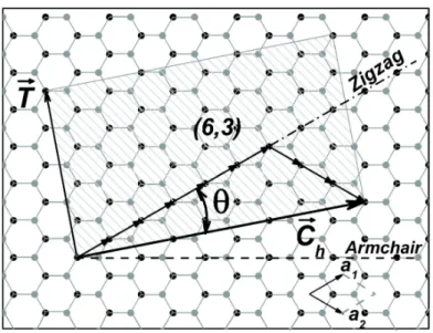
Single-walled carbon nanotubes (SWNT) are a specific arrangement of carbon atoms which can be described as a single graphene sheet rolled up into a cylinder. A SWNT is uniquely characterized by its chiral vector (C~h) [32], which connects the atoms in the
graphene lattice which are seamlessly sewn together during this hypothetical roll-up. In order to obtain a seamless cylinder, C~h must be written as:
~
Ch =n ~a1+m ~a2 (2.1)
wherea~1 and a~2 are the graphene lattice vectors and (n, m) are integers which determine
~
Ch and, therefore, the SWNT’s properties.
AsC~h spans the circumference of the cylinder, we can obtain the SWNT’s diameter
(dt) as:
dt= |
~ Ch|
π =
q
n2|a~
1|2+ 2nm ~a1·a~2
+m2|a~ 2|2
π =
ac−c
π
q
3 n2 +nm+m2
(2.2)
where ac−c = 1.42˚A is the distance between neighboring carbon atoms in graphene and
n, m are integers.
between C~h and a~1:
tanθ = |a~1×C~h|
|a~1·C~h|
= m
√
3
m+ 2n (2.3)
SWNTs with θ= 0◦
or θ= 30◦
are termedzig-zag and armchair, respectively, due to the characteristic shapes of the C-C bonds along these directions. SWNTs with 0◦
< θ <30◦ are termed chiral.
In addition to the circumferential “periodicity” described by C~h, SWNTs are
peri-odic in the traditional sense of the word along their axis. The translation vector T~ which connects two equivalent carbon atoms along the SWNT axis can be written as:
~
T =t1a~1 +t2a~2 (2.4)
for adequate integers t1 and t2. Since T~ is parallel to the SWNT axis, it is perpendicular toC~h:
0 =C~h·T~
0 =nt1|a~1|2+ (nt2+mt1)(a~1·a~2) +mt2|a~2|2
0 =t1(2n+m) +t2(n+ 2m) (2.5)
The smallestt1 and t2 which satisfy (2.5) are:
t1 =
n+ 2m dR
; t2 =−
2n+m dR
(2.6)
where dR is the greatest common divisor of (2n+m,n+ 2m).
The vectors C~h and T~ define the SWNT unit cell, as can be seen in figure 2.1.
The ratio of the area of the SWNT unit cell to that of graphene gives us the number of hexagons (N) in the unit cell of a SWNT:
N = |C~h ×T~|
|a~1 ×a~2|
= 2(n
2 +nm+m2)
dR
(2.7)
Since each hexagon contains two unique carbon atoms, the number of atoms in the SWNT unit cell is 2N.
Thus, we can describe the geometry of a SWNT species either by (n, m), or (dt,θ),
Figure 2.1: The chiral vector C~h and the translation vector T~ for the (6,3) SWNT,
superimposed on a graphene lattice. The dashed rectangle is the (6,3) SWNT unit cell. [33]
2.2
Electronic properties
In much the same way as a SWNTs’ geometrical structure can be described as a graphene lattice over which we superimposed the periodicity of the chiral vectorC~h and the
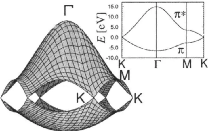
transla-tion vector T~, so too can is its electronic structure, as a first approximation, be described as that of graphene plus the SWNT’s periodicity requirements. This description gives rise to the picture of cutting lines throughout the first Brillouin zone of graphene, which describe the wavevectors available to SWNTs. This approach fails to address the effects of curvature, as well as excitonic and many-body effects, which distort the calculated energy levels, but is enough to give us much insight into the physics at hand.
2.2.1
Tight-binding approximation for graphene
As a first description, let us take graphene’s electronic structure near the Fermi level as calculated by a first neighbors tight-binding approximation. This is a perturbative approach in which the unperturbed eigenvectors are taken as the relevant atomic orbitals – carbon’s 2pz orbital, denoted byϕz here – and the crystal’s potential is the perturbation
cell give rise to two Bloch functions:
ΦA,B =
1 √ M 3 X ℓ=1
ei~k·R~ℓ
ϕz(~r−R~ℓ) (2.8)
whereM is the number of unit cells in the crystal andℓ= 1,2,3 represents the three first neighbors of the relevant carbon atom. The interaction Hamiltonian (H) and the overlap integral matrix for this system are hermitian and symmetric to a changing of indexes
A↔B, and depend only on the sum of the phase factors (f(~k) =P
ℓei~k
·R~ℓ
), being of the form:
H= ε2p −γ0f(~k)
−γ0f⋆(~k) ε2p
!
; S = 1 sf(~k)
sf⋆(~k) 1
!
(2.9)
where ε2p is the energy of the atomic 2pz orbital, γ0 is the nearest-neighbor transfer integral and s is the nearest-neighbor overlap integral.
Obtaining the energy eigenvalues reduces to solving the secular equation:
det H −E(~k)S
= 0 (2.10)
where “det” denotes the determinant. This yields the familiar energy dispersion of graphene, which, with a suitable choice of a reference frame can be written as:
E(~k) = ε2p±γ0w(~k)
1±sw(~k) ; w(~k) =|f(~k)| (2.11)
2.2.2
Quantization in the electronic structure of SWNTs
Now that we have a basic description of the electronic structure of graphene, we must apply the periodicity imposed by the peculiar geometry of SWNTs [16]. Since our ideal SWNT is of infinite length, the wavevector along the direction of the SWNT axis is unconstrained, but the periodicity along the circumference of SWNTs restricts our choice of wavevectors to those that satisfy:
~k·C~h =µ2π (2.12)
for integer µ. Note that |C~h|=πdt and let
~ K1 =
2
dt
~ Ch
|C~h|
; K~2 =
~ T
Figure 2.2: Graphene’s electronic structure close to the Fermi energy, as calculated by the first-neighbor tight-binding approximation. The inset shows shows cuts along high-symmetry lines. Here, γ0 and s are, respectively, 3.033 eV and 0.129. [15, 34]
thus we can write the allowed wavevectors of a SWNT as
~kSWNT =µ ~K1+k ~K2 (2.14)
where µ is an integer and k is a real number. However, since N ~K1 is also a vector of the graphene reciprocal lattice, we can limit the acceptable values to µ= 0,1, . . . , N−1, limiting ourselves to the first Brillouin Zone (BZ). We can limit −π/|T~| < k < π/|T~| in order to stay in the first BZ as well. Thus, we obtain the electronic energy dispersion of SWNTs near the Fermi level as
Eµ(k) =
ε2p±γ0w(~kSWNT) 1±sw(~kSWNT)
(2.15)
This gives rise to N pairs of bands of electronic states in the first BZ. However, N
can be a rather large number, these bands are all within a few eV of each other and cross each other frequently, making the band structure rather confusing, as figure 2.3(b) shows. It is usually more instructive to look at the density of electronic states (g(E)), given by [16]:
g(E) = 2
N
N−1
X
µ=0
Z
dEµ(k)
dk
−1
δ(Eµ(k)−E)dk (2.16)
(a) (b) (c)
Figure 2.3: (a) Allowed electronic states for the (4,2) nanotube superimposed on
graphene’s π and π⋆ bands. Each segment delimited by black bullets represents a single
energy band, as seen in (b). (b) Electronic energy bands for the (4,2) nanotube. (c) Density of electronic states for the band diagram in (b). [15, 34, 35]
SWNT has a non-zero g(E) at the Fermi energy, meaning it is metallic (M). If this is not the case, the SWNT is semiconducting , and is classified as either type 1 (S1, for (2n+m)mod 3 = 1), or type 2 (S2, for (2n+m)mod 3 = 2).
Note that whenever dEµ/dk = 0, g(E) diverges sharply. These local maxima in
density of states (DOS) are called van Hove singularities (vHS) and are responsible for strong electronic transitions, causing SWNTs to behave almost like molecules and not traditional crystals, with discrete, rather than continuous energy levels. The energy dif-ference between the i-th vHS in the valence band and the j-th vHS in the conduction band is dubbed EijM,S, for metallic (M) or semiconducting (S) SWNTs. Due to symmetry considerations, the interaction of light polarized along the SWNT axis – which couples much more strongly to the SWNT’s electrons than other polarizations – can only pro-mote transitions where i = j [16, 32]. The transitions with smallest Eii will occur close
to the graphene K point, where the electronic dispersion is close to linear, and can be approximated by [15]:
Eii(dt, θ)≈a
p dt
+βp
cos 3θ d2
t
(2.17)
where βp takes into account the weak angle dependence of the electronic dispersion, a is
an adjustable parameter and p= 1,2,3,4, . . . for ES
11, E22S, E11M, E33S , . . ..
[36]. The first of these reasons is that we only took into account first neighbors in equation (2.8), when realistically all neighbors must be accounted for. Also, when first calculating the tight-binding approximation for graphene, we used only one electron per carbon atom, since we were only interested in describing in the π bands, which are orthogonal to the
σ bonds in planar graphene [15]. When we rolled up the graphene sheet to form the SWNT, this orthogonality was lost, but we did not take this into account in subsequent expressions. Both of these aspects can be adequately described by the so-called non-orthogonal extended tight-binding (ETB) [37, 38], in which both π- and σ-orbitals are considered, as well as the entire SWNT geometry. First, one considers as many neighbors as is practical for carbon atoms along the SWNT in order to obtain an approximate energy dispersion. Then, while being constrained by the helical symmetry of the specific SWNT one is interested in, the bonding angles between neighboring atoms are allowed to vary, lowering the total energy of the system.
While the ETB can accurately describe the SWNT band structure, it does not describe the excitonic nature of optical transitions in SWNTs [39, 40]. These effects can be calculated within the tight-binding approximation by solving the Bethe-Salpeter equation [41, 42], yielding both the excitonic wavefunctions and transition energies. Since electron-electron repulsion and electron-hole attraction (many-body effects) in SWNTs almost cancel out, they can be taken into account by a logarithmic correction [43, 44], given by:
Eii(dt, θ) =a
p dt
1 +blog c
p/dt
+βp
cos 3θ d2
t
(2.18)
where b is an adjustable parameter and c= 0.812nm−1
. Additionally, since the excitonic contribution is different for small and largeii [36], an extra term ofγp/dt must be added
for transitions higher thanEM 11 [36].
2.3
Vibrational properties
analogous displacement in graphene is merely a translation perpendicular to the graphene plane, with no associated restoring force. A simple model that predicts the basic behavior of the RBM is to consider the oscillation of a thin cylindrical shell of thicknesshsubjected to an inward pressure p(x) =−Kx [45]:
ρ
Y(1−ν
2)∂x(t)
∂t2 + 4
d2
t
x(t) = −(1−ν 2)
Y h Kx(t) (2.19)
where ρ is the cylinder’s density, Y is its Young’s modulus, ν is Poisson’s ratio and x(t) is a small radial displacement. Solving for an oscillating x(t) = exp(iωRBMt) yields:
ωRBM =
s
4Y ρ(1−ν2)
1
d2
t
+ K
ρh
ωRBM =
A dt
p
1 +C·d2
t (2.20)
Where C is an environment-dependent constant [20] and both elasticity theory [46] and experimental measurements [20] give the valueA= 227nm·cm−1
. In free space (p(x) = 0), this is consistent with the familiar behavior of simple oscillating systems, where ω ∝
p
(k/m), since the total mass of the system is proportional to the circumference (m∝ρdt)
Chapter 3
Theoretical background
3.1
Raman scattering
3.1.1
Classical description
Classically, Raman scattering is caused by the modulation of a material’s polarizability due to its vibrations [16]. An incident oscillating electric fieldE~ will induce a polarization
~
P given by:
~
P =↔α ~E (3.1)
where ↔α is the electric polarizability tensor, which is generally a function of the atomic positions of the system. For simplicity, let us assume the system is vibrating in a sin-gle normal vibrational mode Q. The polarizability can then be expanded around the equilibrium positions of the atoms as:
↔
α =↔α0+
∂↔α ∂Q 0
Q+· · · (3.2)
where the derivative is evaluated in the system’s equilibrium configuration. Let Qand E~
be:
Q=Q0cos(ωqt) ; E~ =E~0cos(ωIt) (3.3)
Up to first order, equation (3.1) can then be written as:
~
P =↔α0E~0cos(ωIt) +
∂↔α ∂Q 0
Since 2 cos(a) cos(b) = cos(a+b) + cos(a−b), this becomes:
~
P =↔α0E~0cos(ωIt) +
1 2
∂↔α ∂Q
0
Q0E~0
cos(ωI +ωq)t+ cos(ωI −ωq)t
(3.5)
Thus, an incident monochromatic light of frequencyωI will scatter elastically – Rayleigh
scattering – and inelastically – Raman scattering – provided (∂↔α/∂Q)0 6= 0. The scattered light with frequencies (ωI −ωq) and (ωI +ωq) are referred to as Stokes and anti-Stokes
scattering, respectively.
3.1.2
Quantum mechanical description
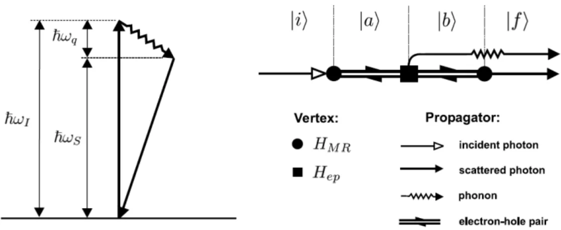
Within the framework of quantum mechanics, Raman scattering in crystals is the inelastic scattering of a photon by a phonon [16]. The most intuitive process that allows this scat-tering in a large crystal is one in which an incident photon of energy ~ωI is absorbed by the crystal, promoting an electron to an excited state. In the Stokes process, before relax-ing back to its ground state, the excited electron emits a phonon, losrelax-ing ~ωq energy. The excited electron then relaxes back to its original state by an optical transition, emitting a scattered photon of energy ~ωS =~ωI −~ωq. This process is illustrated schematically in figure 3.1.
Figure 3.1: Schematic representation of the energy levels and the Feynmann diagram for
The probability for this scattering to occur is described by third-order time-dependent perturbation theory [15, 16, 33, 34, 47, 48, 49]. Here, instead of deducing the expres-sion for the scattering probability, we shall concentrate on an analysis of the description of the system and the use of the end result for calculating RBM Raman intensities in SWNTs. In order to apply perturbation theory, we define the Hamiltonian of the system as H=H0+H1, where:
H0 =HM +HR
H1 =HM R+Hep
(3.6)
such thatH0 ≫ H1 andH1 is treated as a perturbation. Here,HM andHR represent the
Hamiltonians for the matter and radiation parts of the system, respectively, and HM R
and Hep describe the matter-radiation and exciton-phonon couplings, respectively. The
process illustrated in figure 3.1 involves four eigenstates of H0: the initial state |ii, two intermediate states |ai and |bi, and the final state |fi. An eigenstate with eigenvalueEx
is described as |xi = |nI, nS, nq, ϕxi, where nI is the number existing incident photons,
nS is the number of existing scattered photons, nq is the number of existing phonons and
ϕx is the electron’s state. The relevant states and their eigenvalues are then:
|ii = | nI , nS , nq , ϕi i
|ai = | nI −1 , nS , nq , ϕa i
|bi = | nI −1 , nS , nq+ 1 , ϕb i
|fi = | nI −1 , nS+ 1 , nq+ 1 , ϕf i
(3.7)
and their eigenvalues are:
Ei = nI~ωI + nS~ωS + nq~ωq + Eie
Ea = (nI −1)~ωI + nS~ωS + nq~ωq + Eae
Eb = (nI −1)~ωI + nS~ωS + (nq+ 1)~ωq + Ebe
Ef = (nI −1)~ωI + (nS+ 1)~ωS + (nq+ 1)~ωq + Efe
(3.8)
where Ee
x is the energy of the electronic state described by ϕx.
The standard time-dependent perturbation theory formalism gives the Raman cross-section for this process as [47]:
σ =CX
f X a,b
hf|HM R|bihb|Hep|aiha|HM R|ii
(Ei−Ea)(Ei−Eb)
2
δ(Ei−Ef) (3.9)
Whenever the denominator in equation (3.9) approaches zero, the cross-section be-comes very large. This phenomenon is referred to as resonance Raman scattering (RRS) and, when present, dominates over non-resonant scattering. RRS will occur whenever the energy of either the incident or scattered photons matches a SWNT’s Eii optical
transi-tion energy. As written, the right hand side of equatransi-tion (3.9) diverges whenever either resonance condition is achieved, but this is unphysical. Realistically, all of the processes involved in RRS take a finite time to occur, such that Heisenberg’s uncertainty princi-ple restricts the accuracy to which the energy of the excited states is determined. This leads to the addition of a damping factor of iγ in the denominator, which is inversely proportional to the lifetime of the intermediate excited states [16]. This damping factor effectively limits the maximum value of the cross-section, while broadening the resonance profile.
3.1.3
Selection rules for Raman scattering
The Raman cross-section displayed in equation (3.9) will only be different from zero if certain selection rules are respected. The most obvious of these is energy conservation, that is, Ef =Ei. In the limit where the matter-radiation interaction is weak, and where
one extra phonon in the system does not appreciably change the electronic states of the crystal – which is true for large crystals and, specifically, for SWNTs –, the final electronic state ϕf is very close to the initial state ϕi, and the energy due to the new phonon and
scattered photon equals that of the incident photon (~ωI = ~ωS +~ωq), automatically satisfying energy conservation.
Momentum conservation must also be observed throughout the entire process. The maximum momentum transfer from the radiation field to the crystal occurs for backscat-tered light, such that ~kI+~kS =~kq, where kI and kS are the wavenumbers for incident and scattered light, respectively, andkq is the wavenumber for the scattered phonon. The
maximum kq is given by the size of the first BZ, which is π/a, where a is the crystal’s
lattice constant. For SWNTs, this is typically around 108m−1
. For visible light,kI andkS
are of the order of 106m−1
for visible light. Therefore, momentum conservation restricts the phonon’s wavenumber to the vicinity of the center of the first BZ, since we must obey
kq ≪π/a.
hx|H1|yi connecting the initial and final states. As briefly discussed in section 2.2.2, only excitonic transition of the formEii can be promoted by light polarized along the SWNT’s
axis, that is, only some hx|HM R|yi are non-zero [32, 16]. In the specific case of the RBM
phonon, which is a totally symmetric phonon, similar symmetry considerations to those involved in SWNT’s optical transitions restrict the non-zero hx|Hep|yito those that leave
the excitonic state unaltered, or that return the exciton to the original ground state – which is not very likely because of the small energy associated with the RBM phonon.
Taking these facts into account, the dominant terms of equation (3.9) for the scat-tering of light by one RBM phonon can be written as [23]:
σ=C
X a
h0|HM R|aiha|Hep|aiha|HM R|0i
(Elaser −Eii+iγ)(Elaser −Eii−~ωRBM+iγ)
2 (3.10)
where|0iis the SWNT ground state, the sum needs only extend over the bright excitonic states [23] and we assumed for simplicity that the resonance window width is the same for both intermediate states. In the case of the RBM phonon, this assumption is also justified by the fact that the resonances with the incident and scattered photons cannot be experimentally resolved, since they are very close in energy.
3.2
Matrix elements calculations
In order to proceed with the calculation of the Raman cross-section, we must write both the perturbation Hamiltonian H1 and the unperturbed eigenstates explicitly. In section 2.2.2, we presented methods for the calculation of a SWNT’s electronic wavefunctions, and gave a brief description of how to extend the treatment to excitonic wavefunctions. Here, we show the explicit form of the perturbation Hamiltonians, which allow us to obtain the matrix elements needed in equation (3.10).
3.2.1
Matter-radiation interaction Hamiltonian
Classical electromagnetism gives us the Hamiltonian for a spinless electron in the presence of an external electromagnetic field in the Coulomb gauge (∇ ·~ A~ = 0) as [16]:
H =
" |~p|2
2m +V(~r)
#
− me~p·A~+ e 2|A~|2
where~p,m andeare the electron’s momentum, mass and charge,A~andV(~r) are the vec-tor potential and the crystal’s potential, andA~ points along the direction of the oscillating incident electric field. The term in brackets is simply H0 for an electron in the crystal. In the weak field regime, we can neglect the |A~|2 term, such that the matter-radiation interaction becomes:
HM R =−
e
m~p·A~ (3.12)
We are interested in describing an interaction between matter and visible light polarized along a SWNT’s axis. Since the wavelength of visible light is much larger than a SWNT’s diameter, we can neglect the spacial dependence ofA~. A gauge transformation [50] then transforms equation (3.12) into:
HM R =−D~ ·E~ (3.13)
where D~ = e~r is the dipole moment of the electron and E~ is the electric field. This is known as the dipole approximation for matter-radiation interaction, since it also describes the interaction between a pure dipole and an electric field.
Thus, knowledge of the relevant excitonic wavefunctions allows us to obtain the matter-radiation matrix elements involved in calculating the Raman cross-section.
3.2.2
Exciton-phonon interaction Hamiltonian
A deformation of the crystal lattice caused by a vibration changes the electronic structure of a material, introducing a coupling between a crystal’s electronic and vibrational states. Within the Born-Oppenheimer approximation, which considers the electronic Hamiltonian to be independent from the momentum of the nuclei, this coupling is obtained as the difference between the Hamiltonian with atoms displaced by the vibration and with atoms at their equilibrium positions. Since the electron’s momentum contributes equally to both Hamiltonians, this coupling can be written simply as [16, 51]:
Hep =VR~d(~r)−VR~0(~r)≡δV(~r) (3.14)
where VR~d(~r) is the potential caused by the crystal’s atoms at their displaced positions
In order to progress further, we consider the potential of each carbon atom as the Kohn-Sham potential of a neutral pseudo-atom (v(~r−R~ℓ)) at position R~ℓ [16, 51]:
δV(~r) = X
ℓ
v(~r−R~d,ℓ)−v(~r−R~0,ℓ) (3.15)
where the sum is over all the carbon atoms one wishes to include in the approximation. If we consider only small displacements Q~i, such that R~d,ℓ =R~0,ℓ+Q~ℓ, we get:
Hep =δV(~r) =−
X
ℓ
h
~
∇R~ℓv(~r−R~0,ℓ)
i
~ R0,ℓ
·Q~ℓ (3.16)
where the gradient ∇~R~ℓ operates on the coordinates of the atoms. Here, Q~ℓ points along
the phonon eigenvector – radially outward, in the case of the RBM phonon – and has amplitude [16]:
|Q~ℓ|=
s
~nq
NCmCωq
(3.17)
where NC is the total number of carbon atoms in the SWNT, mC is the mass of each
atom, nq is the number of existing phonons and ωq is the phonon’s frequency.
Thus, Hep can be obtained explicitly and knowledge of the relevant excitonic
wave-functions allows us to obtain the exciton-phonon matrix elements involved in calculating the Raman cross-section.
3.2.3
Resonance window width
The resonance window width is determined by the lifetime of the intermediate states in equation (3.10). The lifetime, or its so-called relaxation timeτ, is related to the resonance window width γ by the uncertainty principle as[16]:
γ = ~
τ (3.18)
Even by restricting ourselves only to electron-phonon scattering, we must still con-sider both the creation and absorption of any phonon mode, which can scatter the electron to any available electronic state. Our calculations are reduced by requiring energy and momentum conservations, as well as by the fact that the symmetries of the electronic states and the electron-phonon interaction restricts the allowed scattering processes. The electron-phonon interaction contribution to the resonance window width is given by [16]:
γ = S~ 8πmCdt
X
µ′,k′,q
hϕµ′(k′)|Hep|ϕµ(k)i
2
~ωq(k′
−k)
"
dEµ′(k′)
dk′
#−1
×
× (
δ Eµ′(k′)−Eµ(k)−~ωq(k′−k)
e~ωq(k′−k)/kBT −1 +
+δ Eµ′(k ′
)−Eµ(k) +~ωq(k′ −k)
1−e~ωq(k′−k)/kBT
)
(3.19)
where S is the area of the graphene unit cell, mC is the mass of a carbon atom,dt is the
SWNT diameter, |ϕµ(k)i(|ϕµ′(k′)i is the initial (scattered) electronic state, denoted by
the band index µ(µ′
) and wavenumber k(k′
) and q is the phonon mode. The terms in curly brackets account for energy conservation in the creation or absorption of a phonon with wavenumber (k′
−k) and energy ~ωq(k′
Chapter 4
Experimental details
4.1
Sample selection and preparation
The SWNT sample chosen for this study was produced by water-assisted chemical va-por deposition (CVD) (“super-growth”) [31], yielding a millimeter-long vertical forest of nearly isolated, high quality SWNTs [20, 28, 29, 30, 31]. Its widedt distribution – 1nm to
6nm, as established by high resolution transmission electron microscopy (HRTEM) [52] – along with its high quality SWNTs make this an ideal sample for a calibration of its RBM Raman intensity. The electronic and vibrational characteristics of this sample, as determined by several RRS measurements [20, 29, 30], are close to those expected from ideal free-standing, isolated SWNTs. In particular, it shows the highest Eii reported in
the literature and a strict adherence to the relationωRBM = 227/dtnm·cm−1, indicating
negligible environmental influence on the SWNTs’ behavior.
In order for us to obtain a consistent calibration of the Raman cross-section, the same “super-growth” sample was used for both HRTEM and RRS measurements, but due to the different requirements of the techniques, were prepared in different ways. Raman measurements were performed on the as-grown sample, requiring no special sample preparation. As-grown, the “super-growth” SWNT sample is a carpet-like vertical forest of nearly vertically aligned, mostly isolated SWNTs, supported on a silicon wafer, as shown in figure 4.1 [31].
Figure 4.1: SWNT forest grown with water-assisted CVD. (A) Picture of a 2.5mm tall SWNT forest on a 7mm by 7mm silicon wafer. A matchstick on the left and ruler with millimeter markings on the right are for size reference. (B) Scanning electron microscopy image of the same SWNT forest. Scale bar, 1 mm. (C) SEM image of the SWNT forest ledge. Scale bar, 1 µm. (D) Low-resolution transmission electron microscopy image of the nanotubes. Scale bar, 100 nm. (E) HRTEM image of the SWNTs. Scale bar, 5 nm. From [31].
Figure 4.2: (a) HRTEM image of the SWNT sample. The white circles represent circular fittings to determine the dt. (b) Diameter distribution of the SWNT sample measured
from HRTEM images, with a binning of 0.2nm. The solid line is the sum of two log-normal distributions, represented as dashed lines, plus a small upshift, for clarity.
4.2
High resolution transmission electron microscopy
HRTEM imaging was done by collaborators from NASA Johnson Space Center, USA, using a JEOL 2000 FX instrument equipped with a LaB6 gun, operating at a 160kV acceleration voltage and low enough beam intensity so that no irradiation damage was caused to the sample [53, 54]. Images were recorded with a 4 Megapixel Gatan CCD at a ×250,000 magnification.
Homemade software developed by our collaborators from NASA was used to super-impose circles onto HRTEM images, adjust their diameters and positions until the best fit was achieved and the diameter was then determined. The accuracy of the fitting was estimated to be 0.08nm by repeatedly measuring several nanotubes and observing the spread of the determined diameters. The white circles in figure 4.2(a) are the best fits for seven SWNTs present in this image. Nanotubes with non-circular cross-sections were excluded from the analysis. The diameters of 395 different SWNTs were determined in this fashion, yielding the experimental dt distribution seen in figure 4.2(b), obtained by
binning the measured dt in 0.2nm intervals. Error bars are determined as the standard
deviation of a binomial distribution (SD = p
N p(1−p)), where N = 395 is the sample size and p is the probability of finding a SWNT with a dt that falls within the range of
each bin. The experimentally determined diameter distribution was fitted as the sum of two log-normal distributions [55] defined as:
fi =
Ai
dtσi
exp
−ln
2(d
t/d¯i)
2σ2
i
(4.1)
where A1(A2) = 4(28), ¯d1( ¯d2) = 1.84(3.38)nm, σ1(σ2) = 0.183(0.223) are the parameters obtained from the fitting.
4.3
Raman spectroscopy
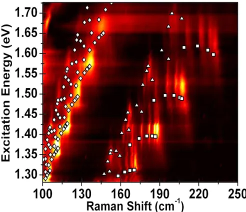
Raman spectra of the sample were obtained with 51 closely spaced laser lines over the 1.28eV to 1.73eV energy range, with a Ti:Sapphire laser and a SPEX triple monochro-mator Raman spectrometer by collaborators from the Chemistry Division of Los Alamos National Laboratory, USA. Laser power densities were kept constant and low enough (25mW with a 10cm focal distance objective) to avoid heating effects.
The Raman spectrum of a standard tylenol sample was measured after each RBM measurement, under the same laser power and focus conditions, and was used for intensity calibration of the RBM spectra. For each laser line, the non-resonant, integrated intensity of the two tylenol Raman peaks at 151cm−1
and 213cm−1
Figure 4.3: Experimentally obtained intensity-calibrated RBM RRS map. Intensity cal-ibration was made by measuring a standard tylenol sample at each laser line. Symbols indicate the transition energies andωRBM for different SWNTs: diamonds forE11M, squares forES1
22 and triangles forES
2
22. Brighter colors indicate higher Raman intensity. Transition energy values were obtained with equation (2.18) and the parameters from [29].
The intensity-calibrated RBM RRS map is shown in figure 4.3, along with symbols indicating the optical transition energies and ωRBM for experimentally observed SWNTs: diamonds represent EM
11, squares represent ES
1
22 and triangles represent ES
2
Chapter 5
Combining HRTEM and Raman
In possession of both the experimental diameter distribution and the intensity-calibrated RBM RRS map of the sample, we can calibrate the Raman cross-section and use this information to determine the diameter distribution of other SWNT samples. However, in order to proceed we must make some assumptions, described in the following section.
5.1
Model assumptions
5.1.1
Population model assumptions
HRTEM measurements determined the diameter distribution of the studied sample, not the relative population of each (n, m) species. Therefore, we assumed that SWNTs of different chiral angles are equally abundant for the “super-growth” process. Though the assumption of chirality-independent growth should not be rigorously true due to structural energy considerations, especially towards very small diameter tubes (dt <1nm) [56, 57],
any under- (over-) estimation of the population of tubes with a certain chiral angle is compensated by an over- (under-) estimation of the RRS RBM cross-section dependence on θ. Therefore, its dt dependence and consequent diameter distribution determination
will still be correct.
Figure 5.1: The modeled population of each nanotube species for the “super-growth” sample. The colorbar represents a species’ chiral angle, in degrees. There is no need to compute the relative population of tubes with dt greater than 4nm because their RBM
frequencies fall too close to the elastically scattered laser light, below the cutoff value of our Raman spectrometer.
given diameter scales linearly with dt. Also, chiral SWNTs (0◦ < θ < 30◦) are twice as
populous as achiral ones, since both right-handed and left-handed isomers contribute to the total Raman intensity of a RBM feature assigned to an (n, m) species. The modeled (n, m) population for the “super-growth” sample is shown in figure 5.1
5.1.2
Raman cross-section model assumptions
The RBM resonance profiles obtained experimentally showed only one resonance peak, thus we were unable to separate the contributions from resonances with the incident and scattered photons. This happened because, as expected from theoretical calculations [22], the resonance window width was larger than the RBM phonon energy. Therefore, we considered the resonance window width γ(n,m) to be the same for both intermediate states.
Note that, since we cannot know the absolute number of SWNTs of a given species in the spectrometer’s focal region, we cannot obtain the absolute Raman cross-section, but rather the relative cross-section, which is related to the absolute cross-section by a multiplicative constant.
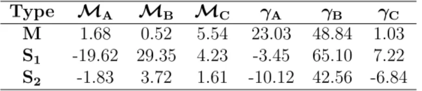
We modeled M(n,m) and γ(n,m) according to the following equations:
M(n,m) =
MA+MB
dt
+ MCcos(3θ)
d2
t
2
γ(n,m) =γA+
γB
dt
+γCcos(3θ)
d2
t
(5.1)
where Mi and γi (i=a,b,c) are adjustable parameters with different values for metallic,
S1 and S2 SWNTs, since theoretical calculations [22, 23] show that the both γ(n,m) and
M(n,m) are very different depending on the SWNT’s type.
These function forms were chosen because they are able to closely reproduce the-oretical calculations available in the literature [22, 23], while still limiting the fitting parameters to an acceptably small number.
5.2
Simulating a resonance Raman map
Each SWNT in the sample contributes to the RBM RRS spectra with a Lorentzian line-shape [16] centered on its RBM frequency, given by:
L(n,m,ω,Elaser) =I(n,m,Elaser)
Γ/2
(ω−ωRBM)2+ (Γ/2)2 (5.2)
where ω is the Raman shift, Γ is the Lorentzian’s full-width at half-maximum – ob-tained experimentally and originating from both the spectrometer’s resolution and the uncertainty in the phonon’s energy – and I(n,m,Elaser) is its total integrated intensity at
excitation laser energyElaser which, once the Raman spectrum has been corrected for the spectrometer’s response, is proportional to the Raman cross-section. In our study, we set Γ = 3cm−1
Type MA MB MC γA γB γC M 1.68 0.52 5.54 23.03 48.84 1.03 S1 -19.62 29.35 4.23 -3.45 65.10 7.22 S2 -1.83 3.72 1.61 -10.12 42.56 -6.84
Table 5.1: Fitted parameters Mi and γi for metallic (M: 2n+m mod 3 = 0),
semicon-ductor type 1 (S1 : 2n+m mod 3 = 1) and type 2 (S2 : 2n+m mod 3 = 2) SWNTs. These parameters are to be used in equation (5.1) with dt in nm, yielding M(n,m) in arbitrary units and γ(n,m) in meV.
From equation (3.10) and our model assumptions, we have:
I(n,m,Elaser)=
M(n,m)
(Elaser −Eii+iγ(n,m))(Elaser −~ωRBM−Eii+iγ(n,m))
2 (5.3)
γ(n,m) and M(n,m) are described by equations (5.1) and are assumed to be constant over the observed energy range.
Since each spectrum (S(ω,Elaser)) is a sum of the individual contributions of all
SWNTs, it can be written as:
S(ω,Elaser) =
X
n,m
Pop(n,m)L(n,m,ω) (5.4)
where Pop(n,m) is the population of the (n, m) nanotube species.
5.3
Results
Using our models for Pop(n,m), γ(n,m) and M(n,m), we simulate a RBM RRS map and
adjust the fitting parameters γi and Mi in order to obtain a least squares fit to the
experimental map, shown in figure 5.2(b). The best values for the fitting parameters, considering the excitonic transitions ES
22 and the lower branch of E11M are listed in table 5.1 for dt in nm, γ(n,m) in meV and M(n,m) in arbitrary units.
Figure 5.2(c) shows the absolute value of the subtraction between the experimental and modeled maps. The overall low intensity of the features in figure 5.2(c) shows that the functions chosen for M(n,m) and γ(n,m) are representative of their experimental behavior. The most pronounced differences between the experimental and the modeled maps come from a region above EM
11 at around 105cm −1
Figure 5.2: RBM RRS maps. (a) Intensity-calibrated experimental RBM RRS map. (b) Modeled RBM RRS map, obtained by using equation (5.4) with the fitting parameters in table 5.1 at the same excitation energies range as (a). (c) Absolute value of the subtraction of the experimental (a) and modeled (b) maps. Symbols indicate the transition energies and ωRBM for different SWNTs: diamonds for E11M, squares for E
S1
22 and triangles forE S2
22. The color bar scale is the same for all three maps. Transition energy values were obtained with equation (2.18) and the parameters from [29].
simulated map. This does not reflect the actual expected Raman intensity values, but is rather an artifact of the simulation: only ES1
22, ES
2
22 and E11M resonances were simulated, while experimentally the ES
33 resonance becomes important in this region.
5.3.1
Comparison of experimental and theoretical
M
and
γ
Figures 5.3(a)–(c) show a comparison of experimental and theoretical [22] values for the resonance window width γ(n,m). Additional theoretical data for metallic SWNTs with
dt > 1.5nm was kindly supplied by J S Park. Of note is the fact that the dependence
of γ(n,m) on chiral angle is similar for both experimental and theoretical values: γM is practically independent of chiral angle, while γS1(γS2) decreases (increases) when going
from zig-zag (Z) to armchair (A) SWNTs. There is very good agreement between theo-retical and experimental γS2
, while there is a slight underestimation (≈ 15meV) on the theoretical calculations forγS1
Figure 5.3: Experimental (solid circles) and theoretical (open circles) [22, 23] γ(n,m) (left) and M(n,m) (right), separated by SWNT type (M,S1,S2). Values are for the E11M and E22S transitions. The letters A and Z indicate armchair-like (θ ≈30◦
) and zig-zag-like (θ ≈0◦ ) SWNTs, respectively. The arrow with θ beside it indicates how the chiral angle varies within a 2n+m = constant family. Additional data for dt >1.5nm SWNTs was kindly
lead to the appearance of an enlarged γ(n,m).
Figures 5.3(d)–(f) show a comparison of experimental and theoretical [23] values for the matrix element M(n,m). Theoretical values were obtained by the following equation:
M(n,m) =
v u u tIref ×
"
γ2 ref +
~
ωRBM 2
2#
(5.5)
where Iref is the intensity per unit length, extracted from FIG.14(a) and FIG.14(c) of reference [23] and γref = 0.06eV is the value assumed in their paper for the resonance window width of all SWNTs. This is obtained by choosing Elaser = Eii +~ωRBM/2 in equation (5.3), which is the laser excitation energy for maximum RRS RBM intensity.
Consistently with the theoretical predictions, our measurements show the largest values for MS1
, while MS2
and MM are of the same order of magnitude. However, we find a steeper dependence of MS1
Chapter 6
Applications
6.1
Determining a sample’s diameter distribution from
Raman RBM spectra
In order to determine the diameter distribution of a SWNT sample from RBM RRS measurements alone, one needs to know the RRS RBM cross-section of each tube in the sample, which includes knowledge of Eii, ωRBM, M(n,m) and γ(n,m). Eii and ωRBM are obtained from the literature for a wide variety of samples and a general picture has been provided for both [20, 30]. The values for M(n,m) and γ(n,m) can be determined by using the fitting parameters provided in table 5.1 in equations (5.1) for theES
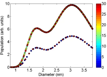
22 and E11M optical transitions, under the assumptions described in section 5.1. We then compare the pre-dicted RRS RBM intensities with the relative intensity ratios obtained from experimental RRS RBM spectra and obtain the diameter distribution of the sample.
The easiest way to compare the experimental intensities with the calculated RRS RBM cross-sections is to compare the experimental spectra with simulated spectra ob-tained by assuming a “dummy” constant diameter distribution, a procedure which is accomplished with the help of the MatLab program SpectraSimulation.m in appendix A. (Important: this program only simulates resonance with ES
Figure 6.1: The modeled population of each nanotube species for the “dummy” popu-lation, with a constant diameter distribution. The colorbar represents a species’ chiral angle, in degrees.
the population of each tube is given by:
Pop(n,m) =
(
1/dt if θ = 0◦ or θ = 30◦
2/dt otherwise
(6.1)
since the density of different (n, m) species scales linearly with dt and chiral tubes have
optical isomers (right-handed and left-handed varieties both of which contribute to the same RBM feature) while achiral tubes do not. This “dummy” population is shown in figure 6.1. Using this “dummy” population, we simulate spectra using the same laser excitation energies that were used experimentally with equation (5.4).
The MatLab program SpectraSimulation.m in appendix A generates a spectrum using the equations and parameters described here for γ(n,m) and M(n,m), taking only
ES
22 and E11M resonances into account. The simulated spectrum is exported as the file
SimSpec[Elaser].txt, where the used excitation energy substitutes the string [Elaser] in the file name. Parameters adequate for SWNT samples with small bundles or SWNTs wrapped in surfactants are used for Eii [36] and ωRBM [20]. All one needs to do is to run the program and state the Elaser that was used and the observed experimental full-width at half-maximum of RBM features (Γ) in cm−1
Figure 6.2: Experimental (blue) spectrum from an alcohol CVD SWNT sample [36] and simulated (red) spectrum, obtained by using equation 5.4 and the “dummy” constant population distribution (see text). The two spectra are normalized by a common RBM peak. As expected, the spectra do not match, since the sample’s diameter distribution is not the same as the “dummy” constant diameter distribution.
Now, compare each experimental RBM spectrum with its simulated counterpart by fitting each of them with the same number of Lorentzians, each centered at the same wavenumber (allowing a freedom of ±3cm−1
, to account for experimental error). The ratio between the areas under these peaks will be directly proportional to the population ratio between the real sample’sdtdistribution and the constant “dummy”dt distribution.
In order to transform the axis from Raman shift (cm−1
) into dt (nm), all one needs
is the correct ωRBM → dt relation. By default, the program uses equation (2.20) with
C = 0.05786nm−2
, which is a constant that fits the data for most of the samples in the literature [20], but may need to be changed depending on your sample. Equation (2.20) can be easily inverted to yield:
dt=
ω2
A2 −C
−1/2
(6.2)
where A= 227nm·cm−1 [20].
Plotting the area ratios versus dt (obtained from the Raman shift by inverting)
Figure 6.3: Black squares represent the integrated area ratios between the Lorentzian peaks used to fit the experimental and simulated spectra in figure 6.2. The red curve is a lognormal [55] fit to the data points. The horizontal axis was transformed from Raman shift (cm−1
) to diameter (nm) by using equation (6.2).
Chapter 7
Final remarks
In summary, we have combined the diameter distribution of a SWNT sample, obtained by high resolution transmission electron microscopy, and a RBM resonance Raman map in order to determine the RBM Raman cross-section of a wide variety of SWNTs. This result allows us to use a sample’s RBM signal in the inverse process, that is, to determine its diameter distribution using only resonance Raman scattering. Due to the very special nature of the “super-growth” sample, the values displayed here are representative of nearly ideal SWNTs, such that the results of this study are useful as experimental data for theorists, as well as a tool which we hope will be useful to experimentalists.
While the procedure described in 6 remains assumption-dependent for a determina-tion of the relative populadetermina-tion of an individual (n, m) species, it is assumption-independent for obtaining the diameter distribution. Notice also that the fitting parametersMi andγi
population for those SWNT which are fully resonant at Elaser (due to an overall increase of the estimated RRS RBM cross-section).
Appendix A
SpectraSimulation.m MatLab
program
%IMPORTANT! This program requires a clean workspace and thus begins with a %"clear" command. Please take the appropriate measures is you wish to save %your workspace before running this program.
%
%This program simulates the Raman RBM spectrum of a SWNT with a constant %diameter distribution, as explained previously. The simulated
%spectrum is exported to the file SimSpec[E_L].txt , where the actual %excitation energy used replaces [E_L] in the file name.
%
%The parameters we use to define the RBM frequency and transition energies %should be valid for SWNT sample with small bundles or of SWNTs wrapped in %surfactancts. If your sample is very different, the parameters defined in %the program should be changed. All of the values that might need to be %changed are commented as such.
%
%We define the basic properties of SWNTs based on their (n,m)
clear
nmin=3; %Tubes from (nmin,0) up to (nmax,nmax) will be considered nmax=40;
C=0.05786; %This constant is used to determine the RBM of the tubes. %PRB 77, 241403 (2008).
%This value is adequate for bundled or wrapped SWNTs and might need to be %changed depending on the sample you are studying.
%First we determine the basic structural properties of the tubes. %Pre-allocating some variables, for better speed
tamn=nmin:nmax; tamk=1:nmax+1; d(tamn,tamk)=0; cosa(tamn,tamk)=0; cos3angle(tamn,tamk)=0; fam(tamn,tamk)=NaN; rbm(tamn,tamk)=0; Eph(tamn,tamk)=0; popconst(tamn,tamk)=0;
for n=nmin:nmax
for k=1:n+1 %m starts from 0 and goes to n m=k-1;
d(n,k)=0.142*(3*(n.^2+n*m+m.^2))^0.5/3.141593;
%tube diameter in nm, using a c-c distance of 0.142 nm
cosa(n,k)=(2*n+m)./(2*((n.^2+n*m+m.^2)^0.5));
cos3angle(n,k)=cos(3*acos(cosa(n,k))); %cos(3*theta) fam(n,k)=mod((2*n+m),3);
rbm(n,k)=227/d(n,k)*sqrt(1+C*d(n,k)^2);
%SWNT’s RBM frequency, in cm^-1.PRB 77, 241403 (2008).
Eph(n,k)=(1.239842E-4)*rbm(n,k);
%hbar*wRBM. Energy of the RBM phonon in eV
if k==1 || k==n+1 %if the tube is achiral popconst(n,k)=1/d(n,k);
%This population is for the "dummy" diameter distribution else %if the tube is chiral
popconst(n,k)=2/d(n,k);
%If the tube is chiral, then left- and right-handed isomers %contribute
end
end end
%Now we determine their transition energies. These values were taken from %PRL 98, 067401 (2007) and should be valid for samples consisting of small %bundles or of SWNTs wrapped with surfactants. For freestanding
%individualized SWNTs (such as those in the "super-growth" sample), the %values of Phys. Stat. Sol. (b) 245, No. 10, 2201-2204 (2008)
%/ DOI 10.1002/pssb.200879625 should be used.
%These values might need to be changed depending on your sample. Please see %PRL 103, 146802 (2009) for a discussion on how the environment can change %the transition energies of tubes.
%The following values are for Eii in units of eV and d(n,k) in nm. Elin=1.049;
%Eii S1
betas(1,1)= 0.05; %E11 betas(1,2)=-0.19; %E22 betas(1,4)= 0.42; %E33 betas(1,5)=-0.4; %E44
%Eii S2
betas(2,1)=-0.07; %E11 betas(2,2)= 0.14; %E22 betas(2,4)=-0.42; %E33 betas(2,5)= 0.4; %E44
%Eii M
betam(1,1)=0.19; %E11M upper branch. Not usually observed in Raman betam(1,2)=-0.19; %E11M lower branch
%Now we calculate the transition energies in units of eV
%First we pre-allocate for speed tamp=1:4;
TE(tamp,tamn,tamk)=0;
for n=nmin:nmax for k=1:n+1
%S2 semiconducting nanotubes transition energies if fam(n,k)==2
TE(1,n,k)= Elin*1/d(n,k).*(1+Elog*log10(lambda*d(n,k)./1))+... betas(2,1)*cos3angle(n,k)./(d(n,k).^2); %E11 S2 TE(2,n,k)= Elin*2/d(n,k).*(1+Elog*log10(lambda*d(n,k)./2))+...
betas(2,2)*cos3angle(n,k)./(d(n,k).^2); %E22 S2 TE(3,n,k)= Elin*4/d(n,k).*(1+Elog*log10(lambda*d(n,k)./4))+...
TE(4,n,k)= Elin*5/d(n,k).*(1+Elog*log10(lambda*d(n,k)./5))+... betas(2,5)*cos3angle(n,k)./(d(n,k).^2)+5/4*... g/(d(n,k)); %E44 S2
end
%S1 semiconducting nanotubes transition energies if fam(n,k)==1
TE(1,n,k)= Elin*1/d(n,k).*(1+Elog*log10(lambda*d(n,k)./1))+... betas(1,1)*cos3angle(n,k)./(d(n,k).^2); %E11 S1 TE(2,n,k)= Elin*2/d(n,k).*(1+Elog*log10(lambda*d(n,k)./2))+...
betas(1,2)*cos3angle(n,k)./(d(n,k).^2); %E22 S1 TE(3,n,k)= Elin*4/d(n,k).*(1+Elog*log10(lambda*d(n,k)./4))+...
betas(1,4)*cos3angle(n,k)./(d(n,k).^2)+g/(d(n,k)); %E33 S1
TE(4,n,k)= Elin*5/d(n,k).*(1+Elog*log10(lambda*d(n,k)./5))+... betas(1,5)*cos3angle(n,k)./(d(n,k).^2)+5/4*... g/(d(n,k)); %E44 S1
end
%M metallic nanotubes if fam(n,k)==0
TE(1,n,k)= Elin*3./d(n,k).*(1+Elog*log10(lambda*d(n,k)./3))... +betam(1,1)*cos3angle(n,k)./d(n,k).^2;
%E11M upper branch
TE(2,n,k)= Elin*3./d(n,k).*(1+Elog*log10(lambda*d(n,k)./3))... +betam(1,2)*cos3angle(n,k)./d(n,k).^2;
%E11M lower branch end
%Now we determine the Raman properties of the tubes, based on the values %from our paper. These are only valid for E22^S and E11^M (lower branch).
%Parameters for the matrix element aMS1=[-19.62 29.35 4.23]’;
aMS2=[ -1.83 3.72 1.61]’; aMM =[ 1.68 0.52 5.54]’;
%Parameters for the resonance window width gamma aGS1=[ -3.45 65.10 7.22]’;
aGS2=[-10.12 42.56 -6.84]’; aGM =[ 23.03 48.84 1.03]’;
%First we pre-allocate for speed M(tamn,tamk)=0;
G(tamn,tamk)=0;
for n=nmin:nmax for k=1:n+1
if fam(n,k)==1 %For S1 tubes
M(n,k)=([1 1/d(n,k) cos3angle(n,k)/d(n,k)^2]*aMS1)^2; G(n,k)=[1 1/d(n,k) cos3angle(n,k)/d(n,k)^2]*aGS1*10^-3; %the 10^-3 factor is so the values are in eV, not in meV elseif fam(n,k)==2 %For S2 tubes
M(n,k)=([1 1/d(n,k) cos3angle(n,k)/d(n,k)^2]*aMS2)^2; G(n,k)=[1 1/d(n,k) cos3angle(n,k)/d(n,k)^2]*aGS2*10^-3; %the 10^-3 factor is so the values are in eV, not in meV elseif fam(n,k)==0 %For metallic tubes
M(n,k)=([1 1/d(n,k) cos3angle(n,k)/d(n,k)^2]*aMM)^2; G(n,k)=[1 1/d(n,k) cos3angle(n,k)/d(n,k)^2]*aGM*10^-3; %the 10^-3 factor is so the values are in eV, not in meV end
end
%Now all we need is to calculate the expected spectrum of this "dummy" SWNT %population
w=10:550; %this is the frequency range of the Raman spectrum in cm^-1. %Feel free to change this according to your preference
EL=input(’Excitation energy in eV = ’); %This is the laser excitation %energy used in eV. This should be changed acording to the laser %excitation energy you used for the experimental spectrum.
FW=input(’FWHM for the RBM Lorentzian in cm^-1 = ’); %This is the %Full-Width at Half-Maximum intensity (in cm^-1) for the tube’s RBM %lorentzian. This should be changed to match the values you get for your %sample.
S(1:max(size(w)))=0; %The spectrum starts as a baseline, at 0 intensity.
%First we pre-allocate for speed I(tamn,tamk)=0;
for n=nmin:nmax for k=1:n+1
I(n,k)= (abs(M(n,k)/((EL-TE(2,n,k)+1i*G(n,k))*(EL-TE(2,n,k)-... Eph(n,k)+1i*G(n,k)))))^2;
for cont=1:max(size(w))
S(cont)=S(cont) + popconst(n,k)*I(n,k)*(FW/2)/((w(cont)-... rbm(n,k))^2+(FW/2)^2);
dlmwrite([’SimSpec’ num2str(EL) ’.txt’], [w’ S’],’ ’)
figure(1) plot(w,S,’k-’)
title([’Simulated spectrum at ’ num2str(EL) ’eV’]) xlabel(’Raman shift (cm^-^1)’)
Bibliography
[1] S.B. Mitra, D. Wu, and B.N. Holmes. An application of nanotechnology in advanced dental materials. The Journal of the American Dental Association, 134(10):1382, 2003.
[2] D. Pum and U.B. Sleytr. The application of bacterial s-layers in molecular nanotech-nology. Trends in Biotechnology, 17(1):8–12, 1999.
[3] L.S. Zhong, J.S. Hu, A.M. Cao, Q. Liu, W.G. Song, and L.J. Wan. 3d flowerlike ceria micro/nanocomposite structure and its application for water treatment and co removal. Chemistry of Materials, 19(7):1648–1655, 2007.
[4] D.K. Tiwari, J. Behari, and P. Sen. Application of nanoparticles in waste water treatment. Carbon Nanotubes, 3(3):417–433, 2008.
[5] P. Guo. Rna nanotechnology: engineering, assembly and applications in detection, gene delivery and therapy. Journal of nanoscience and nanotechnology, 5(12):1964, 2005.
[6] J. Shi, A.R. Votruba, O.C. Farokhzad, and R. Langer. Nanotechnology in drug delivery and tissue engineering: From discovery to applications. Nano letters, 2010. [7] E. Frackowiak and F. Beguin. Electrochemical storage of energy in carbon nanotubes
and nanostructured carbons. Carbon, 40(10):1775–1787, 2002.
[8] M. Terrones, F. Banhart, N. Grobert, J.C. Charlier, H. Terrones, and PM Ajayan. Molecular junctions by joining single-walled carbon nanotubes. Physical review let-ters, 89(7):75505, 2002.
[10] R. Martel, T. Schmidt, HR Shea, T. Hertel, and P. Avouris. Single-and multi-wall carbon nanotube field-effect transistors. Applied Physics Letters, 73:2447, 1998. [11] A. Star, V. Joshi, S. Skarupo, D. Thomas, and J.C.P. Gabriel. Gas sensor array
based on metal-decorated carbon nanotubes. The Journal of Physical Chemistry B, 110(42):21014–21020, 2006.
[12] A.K.T. Lau and D. Hui. The revolutionary creation of new advanced materials carbon nanotube composites. Composites Part B: Engineering, 33(4):263–277, 2002.
[13] D. Tom´anek and R.J. Enbody. Science and application of nanotubes. Springer, 2000. [14] V.N. Popov. Carbon nanotubes: properties and application. Materials Science and
Engineering: R: Reports, 43(3):61–102, 2004.
[15] G. Dresselhaus R. Saito and M. S. Dresselhaus. Physical Properties of Carbon Nan-otubes. Imperial College Press, London, 1998.
[16] R. Saito A. Jorio, M. S. Dresselhaus and G. Dresselhaus. Raman Spectroscopy in Graphene Related Systems. WILEY-VCH, Weinheim, 2011.
[17] Z. Luo, L.D. Pfefferle, G.L. Haller, and F. Papadimitrakopoulos. (n, m) abundance evaluation of single-walled carbon nanotubes by fluorescence and absorption spec-troscopy. Journal of the American Chemical Society, 128(48):15511–15516, 2006. [18] Z. Luo, F. Papadimitrakopoulos, and S.K. Doorn. Bundling effects on the
intensi-ties of second-order raman modes in semiconducting single-walled carbon nanotubes.
Physical Review B, 77(3):035421, 2008.
[19] A. Jorio, R. Saito, J. H. Hafner, C. M. Lieber, M. Hunter, T. McClure, G. Dressel-haus, M. S. DresselDressel-haus,. Physical Review Letters, 86:1118, 2001.
[20] P. T. Araujo, I. O. Maciel, P. B. C. Pesce, M. A. Pimenta, S. K. Doorn, H. Qian, A. Hartschuh, M. Steiner, L. Grigorian, K. Hata, A. Jorio. Nature of the constant factor in the relation between radial breathing mode frequency and tube diameter for single-wall carbon nanotubes. Physical Review B, 77:241403(R), 2008.


![Figure 5.3 : Experimental (solid circles) and theoretical (open circles) [22, 23] γ (n,m) (left) and M (n,m) (right), separated by SWNT type (M,S 1 ,S 2 )](https://thumb-eu.123doks.com/thumbv2/123dok_br/15741375.125555/38.892.112.780.311.764/figure-experimental-solid-circles-theoretical-circles-separated-swnt.webp)
