N.Kapileswar
1and P.Vijaya Santhi
2Dept.of ECE,NRI Engineering College, Pothavarapadu,,,INDIA
Abstract:
This paper presents circuit design for a low power fault secure encoder and decoder system. Memory cells in logic circuits have been protected from soft errors for more than a decade due to increase in soft error rates. In this paper the circuitry around the memory block have been susceptible to soft errors and must be protected from faults. The proposed design uses error correcting codes and ring counter addressing scheme. In the ring counter several new clock gating techniques are proposed to reduce power consumption. A fault secure Encoder and Decoder error free low power logic circuits can be achieved by the proposed design. Simulation results show great improvement in power consumption. Fault secure Encoder and Decoder with clock gated by CG-element consumes approximately half the power of that consumed by the fault free circuit which doesn’t employ clock gating technique
Keywords
:
GC-element, first-in–first-out (FIFO), gated-clock, ring-counter, Double edge triggered(DET ) D flip-flop(DFF ), encoder, decoder, detector, corrector.
1.1
Introduction
circuit reduce error rate and also consumes less power. The existing circuit is just a encoder and decoder with out any fault secure system. The data is stored in memory address generated by binary address decoder. Memory system which can tolerate errors in any part of the system, including the storage unit, encoder and decoder. The information bits are fed into the encoder to encode the information vector. At the output of encoder, error may occur in the code word. The error should be detected and corrected before storing it in memory. The code word is then stored in the memory. Later during operation, the stored code word will be retrieved from the memory unit. Since the code word is susceptible to transient faults while it is stored in the memory, or retrieving the code word. Before decoding the code word, errors should corrected, otherwise the decoded information is not same as the transmitted information. There is need to add detector and corrector circuitry to both encoder and decoder to reduce error rate. To reduce error rate in logic circuits a fault secure encoder and decoder is needed. On adding fault secure design to existing encoder and decoder circuit will increase power consumption.
1.2 Clock gating:
The idea of clock gating is to shut down the clock of any component whenever it is not being used (accessed).on inserting combinational logic along the clock path the unnecessary switching of sequential elements are prevented. Now a days Power consumption has become one of the biggest challenges in high-performance logic circuit design. Designers are thus continuously challenged to come up with innovative ways to reduce power, while trying to meet all the other constraints imposed on the design. Clock gating has been used to reduce dynamic clock power through all levels of the design hierarchy from the top-most chip level down to the individual latch level .On increasing the circuitry in clock path power consumption is reduced. If there is no need of switching some elements in the circuit, then clock is not supplied to those elements. Main concentration is on clock signal because major consumption of power is by clock signal.
2.1 Implementation of fault Secure Encoder and Decoder with clock
gating.
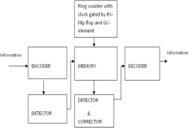
Figure1. Block diagram of fault secure encoder and decoder with clock gating
The information bits are fed into the encoder to encode the information vector, and the fault secure detector of the encoder verifies the validity of the encoded vector. If the detector detects any error, the encoding operation must be redone to generate the correct code word. The code word is then stored in the memory by address generated by ring counter. The ring counter employs clock gating techniques. Later during operation, the stored code word will be retrieved from the memory unit. Since the code word is susceptible to transient faults while it is stored in the memory, the retrieved code-word must be fed into the detector to detect any potential error and possibly to the corrector to recover any erroneous bits. The circuit designed consumes less power and is a fault secure system
2.2 Design Structure of Encoder
An n-bit code-word c, which encodes bit information vector i is generated by multiplying the k-bit information vector with k × n k-bit generator matrix G, i.e.,
c = i · G. Fig.2 shows the generator matrix of (15, 7) code. All the rows of the matrix are cyclic shifts of the first row. This cyclic code generation does not generate a systematic code and the information bits must be decoded from the encoded vector, which is not desirable for our fault-tolerant approach due to the further complication and delay that it adds to the operation[2].
C0c1c2 c3 c4 c5 c6 c7 c8 c9c10c11c12c13c14 I0 1 0 0 0 1 0 1 1 1 0 0 0 0 0 0 I1 0 1 0 0 0 1 0 1 1 1 0 0 0 0 0 I2 0 0 1 0 0 0 1 0 1 1 1 0 0 0 0 I3 0 0 0 1 0 0 0 1 0 1 1 1 0 0 0 I4 0 0 0 0 1 0 0 0 1 0 1 1 1 0 0 I5 0 0 0 0 0 1 0 0 0 1 0 1 1 1 0 I6 0 0 0 0 0 0 1 0 0 0 1 0 1 1 1
The generator matrix of any cyclic code can be converted into systematic form (G = [I : X]) The encoded vector, which is generated by the inner product of the information vector and the generator matrix, consists of information bits followed by parity bits, where each parity bit is simply an inner product of information vector and a column of X, from G = [I : X].
2.3 Design structure of Fault Secure Detector
The core of the detector operation is to generate the syndrome vector, which is basically
implementing the following vector-matrix multiplication on the received encoded vector c and
parity-check matrix H. cHT = S.
Figure 3. Fault-secure detector for (15, 7) code
Therefore each bit of the syndrome vector is the product of C with one row of the parity-check matrix. This product is a linear binary sum over digits of C. where the corresponding digit in the matrix row is 1. This binary sum is implemented with an XOR gate. Fig.3 shows the detector circuit for the (15, 7) code. An error is detected if any of the syndrome bits has a nonzero value. The final error detection signal is implemented by an OR function of all the syndrome bits. The output of this r-input OR gate is the error detector signal.
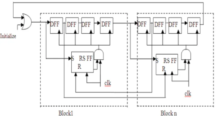
2.4 Design structure of Ring counter with clock gated by R–S flip-flop
By observing the fact that only one of the DFFs in the ring counter is activated at any time, the gated-clock technique has then been proposed to be applied to the DFFs. every eight DFFs in the ring counter are grouped into one block. Then, a “gate” signal is computed for each block to gate the frequently toggled clock signal when the block can be inactive so that unnecessary power
wasted in clock signal transitions is saved. The clock signal is gated by RS-flip flop.
DET DET DET DET Initialize1
clk
DET DET DET DET
clk
Block1 Block n CG
Initialize2
CG
when the input of the first DFF in a block is asserted, it sets the output of the RS-flip flop to “1” at the next clock edge. Thus, the incoming “1” can be trapped in that block and continue to propagate inside the block. On the other hand, the successful propagation of “1” to the first DFF in the next block can henceforth shut down the unnecessary clock signal in the current block. Although some power is indeed saved by gating the clock signal in inactive blocks, the extra RS- flip flops still serve as loading of the clock signal and demand more than necessary clock power.
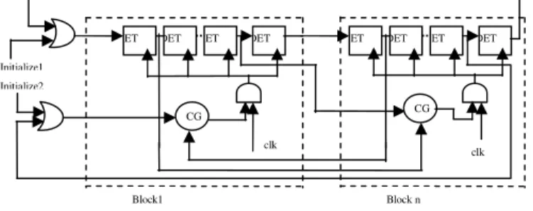
2.5 Design structure of Ring counter with clock gated by CG-element
As the extra RS- flip flops still serve as loading of the clock signal and demand more than necessary clock power, the idea is to replace the RS-flip flop by a CG-element which greatly reduce the power consumption. Additionally, replacing D-flip flops by DET flip-flops reduce the clock rate to half and thus also reduce the power consumption on the clock signal.
Figure 5. Ring counter with clock gated by CG-elements
2.6
Design structure of CG-element
The CG-element is an essential element in asynchronous circuits for handshaking. The logic of the
CG-element is given by C+ =AB+BC+CA
Figure 6. The CG-element
Where A as well as B are its two inputs and C+ as well as C are the next and current outputs. If
A=B, then the next output C+ will be the same as A. Otherwise A B, and C+ remain
are active. The “gate” signal (CKE ) can also be derived from the output of the DET flip-flops in the ring counter.
2.7 Design structure of Corrector
One-step majority logic correction is a fast and relatively compact error-correcting technique.
One-Step majority Logic Corrector: One-step majority logic correction is the procedure that
identifies the correct value of a each bit in the codeword directly from the received codeword; this is in contrast to the general message-passing error correction strategy, which may demand multiple iterations of error diagnosis and trial correction. Avoiding iteration makes the correction latency both small and deterministic. This technique can be implemented serially to provide a compact implementation or in parallel to minimize correction latency. This method consists of two parts: 1) generating a specific set of linear sums of the received vector bits and 2) finding the majority value of the computed linear sums. The majority value indicates the correctness of the code-bit under consideration; if the majority value is 1, the bit is inverted, otherwise it is kept unchanged.
Figure7. Serial one-step majority logic corrector structure
3. Simulation results
3.1 Power analysis
Figure 8. Power consumption of proposed system
0 500 1000 1500 2000 2500 3000
50 70 90 200
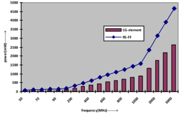
Figure 9. Power consumption of ring counter with RS-FF and CG-element
Table 1 Power consumption of Ring counter
Ring counter structure Power consumption(mW)
Clock gated by RS-flip flop
107mW
Clock gated by CG-element
65mW
Table 2 Power consumption of Ring counter
Voltage (in volts)
Power consumption(mW) Clock gated by
RS-flipflop
Clock gated by CG-element
1.2 28 19
1.4 36 23
1.6 45 28
1.8 55 34
2.0 67 40
2.5 107 65
Table 3 Power consumption of existing and proposed systems
0 500 1000 1500 2000 2500 3000 3500 4000 4500 5000
50 70 90 200 400 600 800 1000 2000 3000
Systems
Power Consumption (mW)
Clock frequency
(MHz)
Delay time (nsec)
Supply voltage (volts)
Without clock gating 105 60 4.990 2.5
Clock gated by RS-flip flop
107 60 4.950 2.5
Clock gated by CG-element
57 60 4.670 2.5
By observing Table 1, Table 2 and Table 3, proposed system with clock gated by CG-element consumes less power than the system with out clock gating and also clock gated by RS-flip flop. For supply voltage of 2.5v and at frequency of 60 MHz, fault secure encoder and decoder without clock gating consumes 105mW of power, with clock gated by RS-flip flop consumes 107 mW and with clock gated by CG-element consumes 57mW of power. The proposed system consumes less power and also has less delay time. The optimum frequency is 60 MHz for the designed system. An important observation from Table 3 is system clock gated by RS-flip flop consumes more power than the system without clock gating because the extra RS-flip flops still serve as loading of the clock signal and demand more than necessary clock power.
3.2 Conclusion
An efficient circuit to reduce soft error’s in logic circuits is designed. Proposed system with clock gated by CG-element consumes less power than the system without clock gating and also clock gated by RS-flip flop. For supply voltage 2.5v and at frequency of 60 MHz, fault secure encoder and decoder without clock gating consumes 105mW of power, with clock gated by RS-flip flop consumes 107 mW and with clock gated by CG-element consumes 57mW of power. The proposed system consumes less power and also has less delay time. The optimum frequency is 60 MHz for the designed system. The system clock gated by RS-flip flop consumes more power than the system without clock gating because the extra RS-flip flops still serve as loading of the clock signal and demand more than necessary clock power. The proposed technique can be used in low power circuit design for multimedia communication devices where long battery life is a crucial factor.
3.3
References
[1] Gallager R.G, “Low-Density Parity-Check Codes”. Cambridge, MA:MIT Press, 1963
[2] McEliece R.J, “The Theory of Information and Coding”. Cambridge, U.K.: Cambridge University Press, 2002.
[3] Tsern.E K and Meng T. H, “A low-power video-rate pyramid VQ decoder,” IEEE J. Solid-State Circuits, Vol. 31, No. 11, Nov. 1996, pp. 1789–1794.
[4] Po-Chun Hsieh, Jing-Siang Jhuang, Pei-Yun Tsai, “A Low-Power Delay Buffer Using Gated Driver Tree” IEEE Trans. Very Large Scale Integr. (VLSI) Syst.,Vol. 17, No. 9, Sep. 2009.
[6] Pastuszak G, “A high-performance architecture for embedded block coding in JPEG 2000,” IEEE Trans. Circuits Syst. Video Technol., Vol. 15, No. 9, Sep. 2005, pp. 1182–1191.
[7] Ryan W. E, “An Introduction to LDPC Codes”, in CRC Handbook for Coding and Signal Processing for Recording Systems (Ed. B. Vasic), CRC Press, 2004.
[8] Karkooti M, Cavallaro J.R, “Semi-Parallel Reconfigurable Architectures for Real-Time LDPC Decoding”, ITCC 2004.
[9] Zhong H, Zhang T, “Design of VLSI Implementation-Oriented LDPC Codes”, IEEE Semiannual Vehicular Technology Conference (VTC), Oct. 2003.
[10] Yeo E, Nikolic B, and Anantharam V, “Architectures and Implementations of Low-Density Parity Check Decoding Algorithms”, IEEE International Midwest Symposium on Circuits and Systems, August. 2002.
[11] Naeimi H and DeHon A, “Fault secure encoder and decoder for memory applications,” in Proc. IEEE Int. Symp. Defect Fault Tolerance VLSI Syst., Sep. 2007, pp. 409–417.
[12] Howard S.L, Gaudet V.C, and Schlegal C, “Soft-Bit Decoding of Regular Low-Density Parity Check Codes”, IEEE Transactions on Circuits and Systems.
[13] Naeimi H and DeHon A, “Fault-tolerant nano-memory with fault secure encoder and decoder,” presented at the Int. Conf. Nano-Netw., Catania, Sicily, Italy, Sep. 2007.
[14] Piestrak S. J, Dandache A, and Monteiro F, “Designing fault-secure parallel encoders for systematic linear error correcting codes,” IEEE Trans. Reliab., vol. 52, no. 4, Jul. 2003, pp. 492–500.