J. Nano- Electron. Phys.
3 (2011) No1, P.117-126 (Sumy State University) 2011 SumDU
117 PACS numbers: 61.05.C – , 68.37.Hk
STRUCTURE, OPTICAL AND ELECTRICAL CHARACTERIZATION OF TIN SELENIDE THIN FILMS DEPOSITED AT ROOM TEMPERATURE
USING THERMAL EVAPORATION METHOD
N. Kumar1, V. Sharma1, U. Parihar1, R. Sachdeva1, N. Padha1, C.J. Panchal2
1 Jammu University, Department of Physics and Electronics,
Ambadkar Road, 180006, Jammu, India E-mail: nareshpadha@yahoo.com
2 M.S. University of Baroda,
Faculty of Technology and Engineering, Vadodara, 390-00 India
Tin Selenide (SnSe) is an important IV-VI compound semiconducting material used for various devices like memory switching, an efficient solar cell and holographic recording systems. SnSe thin films of the thickness of 100 nm were deposited by thermal evaporation method on a Glass substrate at room temperature. The prepared samples were investigated for structural, compositional, morphological and optical characte-rization respectively by using X-ray diffraction analysis (XRD), scanning electron microscopy (SEM) and transmission measurements. Thus deposited films showed a good polycrystalline quality having preferred (111) orientation with uniformly distributed spherical grains having size 16nm.The grown film identified as P- types by hot probe method. The films were found to have direct band transition having an optical bandgap (Eg) of 1.92 eV at room temperature. The temperature depended electrical resistivity ( ) determined by using the two probe method, found to be 390 m at room temperature.
Keywords: TIN SELNIDE, THIN FILMS, SUBSTRATE TEMPERATURE, XRD,
SEM, EDAX, TRANSMISSION ANALYSIS, ELECTRICAL RESISIVITY.
(Received 04 February 2011)
1. INTRODUCTION
2. EXPERIMENT DETAILS
The SnSe thin films studied in this work were grown on a glass substrate at room temperature by using fine-grained pulverized SnSe powder (99.99 %), which was obtained from Alfa Aesar (USA) in a Hind Hivac Vacuum coating unit (model No 12-A4D). The vacuum was maintained at a base pressure of 10 mbar during deposition. The SnSe thin films considered in this study were deposited on soda lime glass substrates with dimensions of approximately 76 25 1 mm3. The quality of the substrate, prior to the
growth of the thin films, is a crucial factor, which influences the material properties of the deposited thin films. Surface defects, such as scratches and dust on the substrate, have an adverse effect on the structural properties of the thin film. In order to obtain glass substrates with a high degree of chemical cleanliness, the following procedure of organic cleaning was used: 1. The glass substrate was rinsed in hydrogen peroxide to remove conta-minants. 2. Substrate was then cleaned, in turn, under vapors of acetone, trichloroethylene, and methanol, respectively. The rate of deposition was 0.3 nm/s and typical thicknesses of the films were 100 nm that were continuously monitored during the deposition using a quartz crystal thickness monitor DTM-101 (Hindhivac, India).
2.1 Characterization Technique
The structural characterization of thin film under investigation was carried out using an X-ray diffractometer (XRD), D-Max-III (Rigaku), in 2 range of 20 °- 60 , at a scan-rate of 0.05°s1, using Cu K ( 0.154 nm) radiation. The surface morphology of the films were studied using a Scanning Electron Microscope (SEM), JSM-5600 (JEOL), operated at 20 kV. To have an idea about the surface elemental composition of the film, Energy Dispersion Analysis by X-ray (EDAX) was carried out by using JEOL EDX Spectrometer (Model No.6360). The optical transmittance measurement was carried out with unpolarized light, at normal incidence, in the photon energy range of 0.8 - 2.5 eV, using the monochromator, CM110, photodetectors, and a lock-in amplifier, SR-530. The whole setup was automated using Lab View (Version 8.2). Temperature depended resistivity measurements for the samples were carried out in a Liquid Nitrogen bath in the temperature range 80 330 K using Keithley Model 6517A programmable electrometer. A Lake Shore model no 340-temperature controller is used for controlling and measuring the temperature (T).
3. RESULTS AND DISCUSSION
STRUCTURE AND CHARACTERIZATION OF TIN SELENIDE… 119
Fig. 1 – XRD Spectra of SnSe thin film (100 nm) at room temperature
A similar preferred orientation of (111) plane in SnSe film was observed by Bhatt et al. [12] and by Dang Tran Quan et al. [14] in the thin films grown by the Vacuum Evaporation Technique and by Singh & Bedi et. al. [15] prepared by Hot Well Epitaxy method. Whereas Teghil et al. [16] observed preferred orientation in the (011) and (200) crystallographic planes in the SnSe thin film prepared by Laser Ablation Method and John et al. [17] repeated (400) plane for films grown by Reactive Evaporation. The various preferred orientation reported for SnSe films indicate that the deposition technique plays an important role for the orientation of SnSe thin film deposition. The XRD data have also found useful for establishing dhkl, Crystallite size (D), Strain ( ) and Dislocation density ( ). The inter-planar spacing dhkl was calculated for the (111) plane using the Bragg’s relation [18]
2 sin
hkl
n
d , (1)
where is the wavelength of the X-ray used, n is the order number and is Bragg’s angle. The crystallite size (D) of the films was calculated from the Debye Scherrer’s formula from the full width at half maximum (FWHM) of the peaks expressed in radians [18]
0.94 cos
D , (2)
where is the FWHM calculated from the (111) plane. The dislocation density ( ) defined as the length of dislocation lines per unit volume of the crystal and calculated by using the formula
2 1
D . (3)
The values of interplaner spacing (d) Grain size (D), and Dislocation density ( ) are calculated from Eq. (1), (2) and (3) are given in table no (1) respectively.
20 30 40 50 60
0 20 40 60 80 100 120
(4
11
)
(3
11
)
(1
1
1)
(0
1
1
)
In
te
n
s
it
y
2
Table 1 – Structural parameter of SnSe film deposited on glass substrate at room temperature
Substrate Temperature
( C)
Plane (hkl)
Thickness (Å), nm
Interplanar Spacing(d),
Lattice
const., FWHM (Degrees)
Grain Size(D)
(nm)
Dislocation density
(1010 line\m2) Room
Temperature (111) 100 3.03807 5.25558 0.50742 16 0.05896
The analysis of the diffraction patterns also suggests that the SnSe thin-film deposited at room temperature has orthorhombic structure with lattice parameters a b 0.431 nm and c 0.540 nm belonging to the D2h16 space group while the interplaner spacing d value corresponding to the (111) prominent peak is determined to be 3.03 nm which is in accordance with the d value given in the JCPDS data. Also, the position and intensities of the peaks are consistence with JCPDS card File (No. 32-1392). This shows that the film grown at room temperature has good crystallinity.
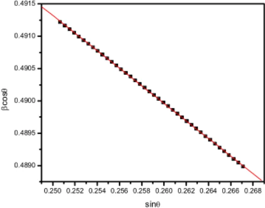
The strain ( ), particle size (D) and dislocation density ( ) are also calculated by using the Williamson and Smallman relation (19)
cos sin
D , (4)
where is the wavelength of the radiation used (0.15418 nm), the full width at half maximum, and the angle of diffraction.
0.250 0.252 0.254 0.256 0.258 0.260 0.262 0.264 0.266 0.268 0.4890
0.4895 0.4900 0.4905 0.4910 0.4915
c
o
s
sin
Fig. 2 – Plot of cos vs sin for a SnSe thin films of thickness of 100 nm grown at room temperature
STRUCTURE AND CHARACTERIZATION OF TIN SELENIDE… 121
Table 2 – Micro-structural parameters of SnSe films deposited on glass substrate at room temperature
Substrate Temperature
C
Plane (hkl)
Thickness (Å), nm
Average internal strain ( )
FWHM (Degrees)
Average grain size, nm
Dislocation density
(1010 line\m2) Room
Temperature (111) 100 0.13543 0.50742 16 0.05896
3.1 Composition analysis
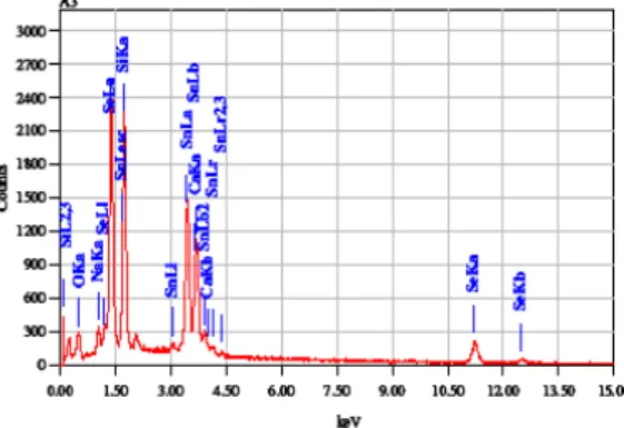
The composition analysis of the SnSe thin films has been carried out using Energy dispersive analysis of X-ray (EDAX) recorded in the binding energy range 0 - 20 KeV. The EDAX spectra of SnSe thin film shown in Fig. 3 revealed that SnSe contents depend critically on the growth condition and technique used for deposition of thin films. From the EDAX patterns, the presence of Sn and Se peaks is observed and some other peaks are also observed which corresponds to Si, Na, Ca and O that can be attributed to the glass substrate used [21]. The atomic mass percentages SnSe of the films grown at room temperature have been found to be 31.78 and 33.18 respectively. This shows that the film grown at room temperature is slightly rich in Selenium and is nearly stoichiometric in nature, which is in agreement with the reported value of Tomkiewicz et al. (22) and Skyllas kazcos and Miller [23].
Fig. 3 – EDAX Spectra of SnSe thin film (100 nm) deposited at room temperature on the glass substrate
3.2 SEM Analysis
Fig. 4 – Scanning Electron Micrograph of SnSe thin film (100 nm thick) deposited on the glass substrate at room temperature
3.3 Optical Analysis
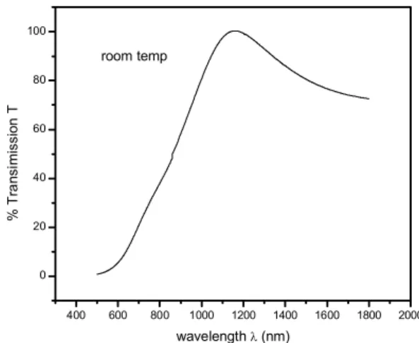
Optical studies are obtained by recording the transmission spectra of the thin film deposited on glass substrate in the wavelength range of 500 nm to 1500 nm at room temperature. Fig. 5 shows the optical transmission spectra of SnSe thin film deposited at room temperature. Film shows more than 50 % transmission for wavelength longer than 800 nm which is an indication of good crystallinity of the film.
400 600 800 1000 1200 1400 1600 1800 2000 0
20 40 60 80 100
%
T
ra
n
s
im
is
s
io
n
T
wavelength (nm) room temp
Fig. 5 – Transmission spectra of SnSe thin film at room temperature
The optical absorption coefficient was calculated using Lambert law (24)
0
ln I 2.303A d
I , (5)
STRUCTURE AND CHARACTERIZATION OF TIN SELENIDE… 123
The spectral dependence of absorption coefficient i.e the function a f(hn) at room temperatures is shown in Fig. (6). The relation between absorption coefficient ( h )2 and the photon energy h is given by the equation of Bardeen et al (25)
h B(h – Eg)x, (6)
where B is the edge width parameter; x 0.5 for direct transition, x 1.5 for allowed and forbidden transition respectively, x 2 for indirect allowed transition, x 3 for indirect forbidden allowed transition. It is observed that the spectral variation can be described by equation (6) with x ½.
0.6 0.8 1.0 1.2 1.4 1.6 1.8 2.0 2.2 2.4 2.6 0.00E+000
5.00E+010 1.00E+011 1.50E+011 2.00E+011 2.50E+011 3.00E+011
room temp band Gap = 1.92eV
(
h
)
2
e
V
2 -c
m
-2
Photon energy h (eV)
Fig. 6 – Plot of ( h )2 vs photon energy h of SnSe thin film (100 nm)
The optical band gap Eg of the film was determine from the extrapolation
of the linear fit plot of ( h )2 versus at h 0 and was found to be 1.92 eV at room temperature. Linearity of above plot indicates that the material is of the direct band gap. The values of bands gap in agreement with the band gap values as repeated by other Nariya et al reported an indirect band gap value of 1.0 eV by direct vapor transport technique [26], Zulkarnain et al reported an indirect band gap of 1.25 eV by a combination of chemical precipitation and vacuum evaporation technique [27], N.A. Okereke et al. reported reported an indirect band gap of 1.5 eV by a combination of chemical deposition [31] and Matthew et al. reported the direct band gap value of 1.71 eV by a Solution-Phase Synthesis [32].
3.4 Electrical Analysis
Fig. 5 shows the variation of electrical resistivity with change in temperature. The decrease in resistivity as temperature increase shows the semiconducting nature of the film [30].
50 100 150 200 250 300 350 10
100 1000 10000 100000 1000000 1E7 1E8 1E9 1E10
R
e
s
is
ti
v
it
y
l
o
g
(
)
Temperature (K)
Fig. 7 – Temperature depended Electrical Resistivity measurement of SnSe thin film using two probe method in the temperature range from 325 K down to 80 K
The electrical resistivity of a polycrystalline thin film sample is a complex phenomenon, involving charge-carriers transport through both the “bulk-like” part of the semiconductor crystals and through the inter-crystalline (grain) boundaries. In the literature [28] the temperature dependence of the semiconductor material’s resistivity is expressed by the equation no (7)
0exp
a
b
E
R R
K T , (7)
where R0 is the pre-exponential factor, Ea is the activation energy for this thermally activated process and Kb is the Boltzmann constant.
0 .0 0 4 0 . 0 0 8 0 .0 1 2 0
5 1 0 1 5
A = -9 .6 6 18 9 + /- 0. 08 4 7 1 B = 2 94 7 .8 9 2 1 6+ /- 16 .8 98 8 3 E g = 0 .2 6 8 e V
ln
(
R
/R
3
0
0
K
)
1 /T (K- 1)
Fig. 8 – Plot of ln(R/R300K) versus 1/T for a SnSe thin film of thickness of 100 nm grown at 350 K temperature
STRUCTURE AND CHARACTERIZATION OF TIN SELENIDE… 125
conductivity it is enough to measure the electrical resistance R since we are interested in the slope of the linear-least square fit only. So, the temperature dependence of resistance of SnSe thin films has been studied by measuring the resistance in the temperature range 80 - 330 K using the Keithley Model 6521 scanner card. Depending on the sample resistivity, a voltage limit was adjusted to obtain reliable data. The data collected was normally repeated for reproducibility check. After stabilizing to the desired temperature, the resistance values were normally recorded three times and their mean was noted. Once the dimensional factors were determined for each sample, the resistivity values were calculated. The resistivity thus obtained had an estimated error within 5%.The values of the activation energy for electrical conduction closely correspond with the measurements performed by another group [29].
4. CONCLUSION
Tin Selenide thin films have been successfully grown by thermal evaporation technique onto glass substrate held at 3050 K. X-ray Diffraction analysis confirmed that the deposited SnSe thin films were polycrystalline in nature having Orthorhombic structure with preferred orientation of grains along the (111) direction. Various structural parameters such as crystalline size, Strain and Dislocation Density are calculated from the XRD Spectra. SEM studies reveal that the SnSe films exhibited uniformly distributed grain over the entire surface of the substrate. The average sizes of the grains are found to be 16 nm. The presences of elemental composition were confirmed from EDAX analysis. Optical Transmittance measurements indicate the deposited film have a direct bandgap of 1.92 eV which confirms the formation of well crystallized SnSe films. Activation energy calculated from temperature dependent resistivity measurements was found to be 0.268 eV which correspond to shallow donor level near conduction band.
REFERENCES
1. A. Agarwal, S.H. Chaki, D. Lakshminarayan, Mater. Lett. 61, 5188 (2007). 2. A. Agarwal, P.H. Trivedi, D. Lakshminarayan, Cryst. Res. Technol. 40, 789
(2005).
3. Z. Zainal, S. Nagalingam, A. Kassim, M.Z. Hussian, W.M.M. Yunus, Sol. Energy Mater. Sol. Cells81 No2, 261 (2004).
4. V.E. Drozd, I.O. Nikiforova, V.B. Bogevolnov, A.M. Yafyasov, E.O. Filatova, D. Papazoglou, J. Phys. D: Appl. Phys 42, 125306 (2009).
5. Z. Zainal, N. Saravanan, K. Anuar, M.Z. Hussein, and W.M.M. Yunus, Mater. Sci. Eng. B 107, 181 (2004).
6. D. P. Padiyan, A. Marikani, and K.R. Murali, Cryst. Res. Technol.35, 949 (2000). 7. N.D. Boscher, C.J. Carmalt, R.G. Palgrave, and I.P. Parkin, Thin Solid Films
516, 4750 (2008).
8. L. Amalraj, M. Jayachandran, and C. Sanjeeviraja, Mat. Res. Bull.39, 2193 (2004). 9. Z. Zainal, A. Jimale Ali, A. Kassim, and M.Z. Hussein, Sol. Energy Mater. Sol.
Cells79 No2, 125 (2003).
10. G.H. Chandra, J. Naveen Kumar, N. Madusudhana Rao, S. Uthanna, J. Cryst. Growth306, 68 (2007).
11. T. Subba Rao, B.K. Samantharay and A.K. Chaudhuri, J. Mat Sci Lett 4, 743 (1985).
13. R.D. Engelken, A.K. Berry, Doren Van, J.L.T.P. Boone and A.J. Shanazary,
Electro Chem. Soc.133, 581 (1986).
14. D.T. Quan, phys. status solidi a86, 421 (1984). 15. J.P. Singh, R.K. Bedi, J. Appl. Phys.68, 2776 (1990).
16. R. Teghil, A. Santagata, V. Marotta, S. Orlando, G. Pizzella, A. Giardini-Guidoni, A. Mele, Appl. Surf. Sci.90, 505 (1995).
17. K.J. John, B. Pradeep, E. Mathal, J. Matter. Sci.29, 1581 (1994).
18. B.D. Cullity, Elements of X-ray Diffraction (Addison-Wesley: Reading, M.A.: 1972).
19. G.B. Williamson, R.C. Smallman, Phil. Mag.1, 34 (1956).
20. B.D. Cullity, Elements of X-ray Diffraction (Addison-Wesley Publ. Co.: California: 1956).
21. S. Prabahar, M. Bhanam, J. Cryst. Growth285, 41 (2005).
22. M. Skyllas Kazcos, B. Miller, J. Electrochem. Soc. 127, 2016 (1980). 23. R.B. Kale, C.D. Lokhande, Semicond. Sci. Tech.20, 1 (2004). 24. A. Adachi, A. Kudo, T. Sakata, Bull. Clm. Soc. Jpn.68, 3283 (1995).
25. J. Bardeen, F.J. Blatt, L.H. Hall, R. Brechenridge, B. Russel, T. Hahn, Photoconductivity Conf. (Wiley: New York: 1956).
26. B.B. Nariya, A.K. Dasadia, M.K. Bhayan, A.J. Patel, A.R. Jani, Chalcogenide Lett. 6, 549 (2009).
27. Z. Zulkarnain, J. Ali, K. Anuar, H. Mohd Zobir, Malaysian Journal of Analytical Sciences 7, 197 (2001).
28. A.J. Moulson, Electroceramics (Wiley: USA: 1990).
29. K. Chung, D. Wamwangi, M. Woda, M. Wuttig and W. Bensch, J Appl. Phys. 103, 083523 (2008).
30. N. Kumar, V. Sharma, N. Padha, N.M. Shah, M.S. Desai, C.J. Panchal, I.Yu. Protsenko, Cryst. Res. Technol.45, 53 (2010).
31. N.A. Okereke, A.J. Ekpunobi, Chalcogenide Lett. 7, 531 (2010).