J. Nano- Electron. Phys.
3 (2011) No1, P. 507-513 (Sumy State University) 2011 SumDU
507
PACS numbers: 68.37. Hk, 81.15.Ef, 68.55.aq, 78.66. – w, 61.05.C –
GROWTH STRUCTURAL AND OPTICAL PROPERTIES OF THE THERMALLY EVAPORATED TIN DISELENIDE (SnSe2) THIN FILMS
R. Sachdeva1,M. Sharma1, A. Devi1, U. Parihar1, N. Kumar1,
N. Padha1*, C.J. Panchal2
1 University of Jammu,
Baba Sahib Ambedker Road, 180006, Jammu Tawi, India E-mail: [email protected]
2 M. S. University of Baroda
390001, Vadodara, India
Tin diselenide (SnSe2) compound was prepared by melt-quenching technique from its constituent elements. The phase structure and composition of the chemical constituents present in the bulk has been determined using X-ray diffraction (XRD) and energy dispersion X-ray analysis (EDAX) respectively. SnSe2 thin films were grown using direct thermal evaporation of SnSe2 compound material on chemically cleaned glass substrate, which were held at different substrate temperatures. X-ray diffraction and Scanning Electron Microscopy (SEM) were used to examine structure and surface morphology of the films. The investigations show that the films grown above 150 C are single phase and polycrystalline in nature. VIS-IR Spectra of the films were recorded in the wavelength range 380 nm to 1300 nm. The data has been analyzed to find optical parameters like absorption coefficient and energy bandgap.
Keywords: SnSe2, THIN FILMS, THERMAL EVAPORATION, SEM, XRD, TRAMS-MITTANCE MEASUREMENTS.
(Received 04 February 2011, in final form 19 June 2011)
1. INTRODUCTION
508 R. SACHDEVA, M. SHARMA, A. DEVI, ET AL.
2. EXPERIMENTAL DETAILS 2.1 Film Preparation
Thin films of tin diselenide were prepared from the bulk material by a thermal evaporation technique on chemically-cleaned glass substrates at different temperatures ranging from RT to 300 C at a reduced pressure of 10 – 5 Torr (1 Torr 1.333 10 – 2Pa) using the conventional vacuum coating
unit (Hind Hivac Co. Ltd., India). Molybdenum boat was used to evaporate SnSe2 powder. The deposition rate of 0.4-0.6 nm/s for typical thickness of
100 nm was continuously monitored during the deposition using a quartz crystal thickness monitor DTM-101 (Hind Hi Vac., India). The substrate temperature was measured using chromel-alumel thermocouple kept in good thermal contact with the substrate.
2.2 Characterization techniques
The structural characterization of the thermally evaporated SnSe2 thin
films were carried out using an X-ray diffractometer (Philips X’Pert PRO MRD HR X-Ray Diffraction System) in 2θ range of 10 to 80 at a scan rate of 0.05 s – 1 using CuK radiation. The morphology of the film was
studied by scanning electron microscopy (FEI, Quanta 200F, Netherland). The optical transmittance measurements used to determine the absorption coefficient and the optical bandgap (Eg) were carried out using monochrometer (CM110), photodetectors (New port 818-SL and 818-SR) and lock in amplifier. The whole setup was automated using LabVIEW8.2.
3. RESULTS AND DISCUSSIONS
3.1 Structural characterization of SnSe2 thin films
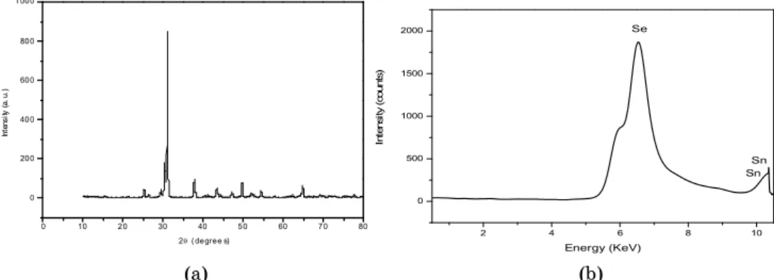
Fig. 1 a shows the X-ray diffraction pattern of the synthesized SnSe2 powder.
The sharp peaks present in X-ray diffraction pattern indicate that the prepared SnSe2 has hexagonal structure and polycrystalline in nature [10]. EDAX analysis of the compound was done to confirm the stoichiometric. The EDAX pattern of the powder is also shown in Fig. 1 b. Table 1 presents EDAX data which indicates the stoichiometry of elements which verifies formation of SnSe2 phase in synthesized powder.
0 10 20 30 40 50 60 70 80 0 200 400 600 800 1000
2 (degree s)
In te ns ity (a . u .)
2 4 6 8 10
0 500 1000 1500 2000 In te ns ity (c ou nt s) Energy (KeV) Sn Se Sn
(a) (b)
GROWTH STRUCTURAL AND OPTICAL PROPERTIES OF... 509
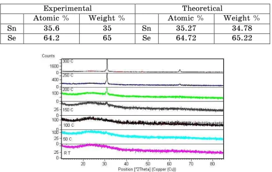
X-ray diffraction pattern of the SnSe2 thin films deposited at different
substrate temperatures are shown in Fig. 2. From the figure, it is clear that the substrate temperature has significant influence on the quality of the films. For instance, the films grown at room temperature to 150 C are amorphous in nature.
Table 1 – Experimental and theoretical EDAX data of the prepared SnSe2
compound
Experimental Theoretical
Atomic % Weight % Atomic % Weight %
Sn 35.6 35 Sn 35.27 34.78
Se 64.2 65 Se 64.72 65.22
Fig. 2 –The XRD pattern of SnSe2 films at different substrate temperatures
The initialization of the crystalline phase has started when the substrate temperature increased above 150 C. Further, thin films grown at substrate temperature 150-300 C are single phase having orientation of the grains in (101) plane. The crystallite size of the films deposited at different substrate temperatures were calculated using the well known Scherrer’s formula [11].
0.9 cos
d B
(1)
Where is the wavelength of CuK ( 1.5418 Å) radiation, B is the full-width half-maximum (FWHM). The position and FWHM of the (101) peak, along with the calculated values of the crystallite size for films grown at different substrate temperatures are shown in Table 2.
510 R. SACHDEVA, M. SHARMA, A. DEVI, ET AL.
Table 2 – Position of (101) peak, Crystallite size and FWHM of SnSe2 films grown at different temperatures
Substrate Temperature
(Ts), C
Position of peak
(101), degrees FWHM, radians
Crystallite size, nm
150 30.9069 0.44 31.20
200 30.9069 0.39 35.15
250 30.9658 0.29 46.80
300 31.0339 0.12 111.44
Fig. 3 – SEM images of the films grown at 150 C (a), 200 C (b), 250 C (c), 300 C (d)
3.2 Optical characterization
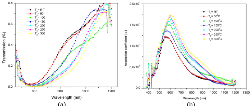
3.2.1 Transmission Spectra and Absorption Coefficient
The plots of transmission spectra versus wavelength and absorption coefficient versus wavelength are shown in Fig. 4.
(a) (b)
GROWTH STRUCTURAL AND OPTICAL PROPERTIES OF... 511
(a) (b)
Fig. 4 – Transmission spectra (a) and the absorption coefficient (b) of SnSe2 thin films deposited at different substrate temperatures
3.2.2 Absorption coefficient and energy bandgap
Transmission spectra in the wavelength range 380 nm to 1300 nm at normal incidence of as-deposited (at different substrate temperatures) films were recorded. From these spectral data optical absorption coefficient was calculated using Lambert’s law [12],
0
ln I 2.303A d
I
(2)
where I and I0 are the intensity of the incident and transmitted light, A is
the optical absorbance and d is the film thickness. The absorption coefficient was found to follow the relation [13],
1 2g
h B h E
, (3)
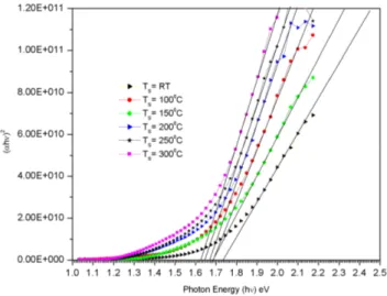
where B is a constant and Eg is the bandgap energy. Plot of (h)2 versus the photon energy (h) for films deposited at different substrate temperatures is shown in Fig. 5.
Linearity of the plot indicates that the material is of direct bandgap [14]. The values of bandgap estimated from the plot of the films are shown in Table 3.
Table 3 – Variation of bandgap with substrate temperature
Substrate Temperature Ts,C Eg, eV
RT 1.72
50 1.72
100 1.67
150 1.67
200 1.68
250 1.65
512 R. SACHDEVA, M. SHARMA, A. DEVI, ET AL.
Fig. 5 – Plot of images of (h)2 versus the photon energy (h) of the SnSe2films
The bandgap calculated on the basis of this analysis is found to decrease with increase in the substrate temperature and vary from 1.62 eV to 1.72 eV in the manner as shown in Table 3. These values are in good agreement with the bandgap values as reported by many earlier workers [15-17]. The decrease in the direct bandgap value with increasing temperature in semiconductors was studied by Olguin et al. [18]. The authors reported two main reasons for this behavior. The first reason for the direct bandgap shift is the effect of thermal expansion of the lattice, which relates to the change of electron energies with volume. The second reason is the direct renormalization of the band energies due to temperature dependence of the electron-phonon interactions.
4. CONCLUSION
In this work, SnSe2 thin films were prepared from stoichiometric compound
using direct thermal evaporation method. X-ray diffraction and SEM analyses revealed that the Thin Film grain size increased with the substrate temperature and it has provided maximum value of 111.4 nm at the substrate temperature of 300 C having preferred orientation in the (101) direction. The transmission spectrum was analyzed to obtain optical parameters. The films have absorption coefficient in the range 10 to 20 and provides direct bandgap which decreases with increase in substrate temperature. Typical value of the bandgap which has been obtained at 300 C is 1.62 eV.
REFERENCES
1. M. Ohring, The material and science of thin films (New York, FRG: Academic press: 1992).
GROWTH STRUCTURAL AND OPTICAL PROPERTIES OF... 513
3. A. Agarwal, M.N.E. Vashi, D. Lakshminarayana, N.M. Batra, J. Mater. Sci. Mater. El. 11, 67 (2000).
4. T. Subba Rao, A.K. Chaudhuri, J. Phys.: D Appl. Phys.18, L35 (1985). 5. T. Subba Rao, A.K. Chaudhuri, J. Phys.: D Appl. Phys.19, 861 (1986). 6. D.P. Padiyan, A. Marikani, K.R. Murali, Cryst. Res. Technol. 35, 949 (2000). 7. R.D. Engelken, A.K. Berry, T.P. Van Qoren, J.L. Boone, A. Shahnazary,
J. Electrochem. Soc. 133, 581 (1986).
8. B. Subramanian, T. Mahalingam, C. Sanjeeviraja, M. Jayachandran, M.J. Chockalingam, Thin Solid Films 357, 119 (1999).
9. J.P. Singh, R.K. Bedi, J. Appl. Phys. 68, 2776 (1990).
10.Evans, Hazelwood, Ph. D Thesis R. Hazelwood Reading, Private Communication, (1970).
11.B.D. Cullity, Elements of X-ray Differaction (London, FRG: Addison Willy: 1978).
12.A. Adachi, A. Kudo, T. Sakata, Bull. Cem. Soc. Jpn. 68, 3283 (1995).
13.J.I. Pankove, Optical processes in Semiconductors, (Englewood Cliffs: Prentice Hall: NJ: 1971).
14.N.M. Shah, J.R. Ray, K.J. Patel, V.A. Kheraj, M.S. Desai, C.J. Panchal, B. Rehani, Thin Solid Films 517, 3639 (2009).
15.G. Domingo, R.S. Itoga, C.R. Kannewurf, Phys. Rev. 143, 536 (1966). 16.V.P. Bhatt, K. Gireesan, C.F. Desai, Cryst. Res. Technol. 25, 209 (1990). 17.M.M. El-Nahass, J. Mater. Sci. 27, 6597 (1992).