Instituto de Ciˆ
encias Exatas
Departamento de F´ısica
Laborat´
orio de Estrutura Eletrˆ
onica
L´ıdia Carvalho Gomes
Two-Dimensional Materials: Electronic
and Structural Properties of Defective
Graphene and Boron Nitride from First
Principles.
Tese de Doutorado
L´ıdia Carvalho Gomes
Two-Dimensional Materials: Electronic
and Structural Properties of Defective
Graphene and Boron Nitride from First
Principles.
Orientador:
Prof. Ricardo Wagner Nunes
Tese apresentada ao Programa de P´
os-gradua¸c˜
ao do
Departa-mento de F´ısica da Universidade Federal de Minas Gerais como
requisito parcial `
a obten¸c˜
ao do grau de Doutor em F´ısica.
Aos meus pais Jo˜ao e Cleusa, e `a minha irm˜a La´ıs, pelo amor imenso e pelo apoio. Mais
que minha fam´ılia s˜ao mesmo anjos na minha vida, a quem sempre dedicarei cada passo novo que eu der. Amo vocˆes.
A todos os tios e tias, primos e primas, vovˆos e vov´os. Mais que fam´ılia no nome ou no sangue, ´e fam´ılia de cora¸c˜ao, que torce e est´a presente a todo momento. Em especial `a
Tia Lˆe, que esteve em meus pensamentos a cada palavra colocada aqui.
Ao Ricardo, pelo exemplo profissional e humano. Muito obrigada pela orienta¸c˜ao sempre
paciente e presente. Obrigada pelos minutos r´apidos de tirar d´uvidas que sempre viraram verdadeiras aulas de f´ısica. Esses anos foram certamente de valor imenso na minha
forma¸c˜ao.
`
A Simone, ao M´ario e ao H´elio Chacham, pela amizade, pelas colabora¸c˜oes, discuss˜oes, e por estarem sempre abertos a nos dar apoio quando preciso.
A todos os amigos desse lado do mundo: Aninha, Alana, D´ebora, L´ıgia, Vivi, Regi, Mangos, Medeir˜ao, Matheus, Ananias, Emilson, Daniel, Davi, Ingrid, Campˆo, Jena ...
Enfim, a todos aqueles (e foram muitos) que de alguma maneira contribu´ıram para que esses quatro anos tenham valido a pena.
Ao Antˆonio H´elio, pela oportunidade de crescimento profissional e pessoal. Muito obri-gada pela confian¸ca, pelo incentivo e pelas portas abertas. Isso ter´a sempre uma
im-portˆancia enorme para mim.
`
A minha fam´ılia portuguesa/singapurense: N´adia, Manuel, Z´e Carlos, Inˆes, F´abio,
Miguel, Paula, Alan, Alexandra, Tˆania e V´ıtor. Ao Jo˜ao Nuno, pelo carinho e apoio todo especiais. Sem vocˆes meu ´ultimo ano n˜ao teria sido t˜ao sorridente e acolhedor. Obrigada de todo o cora¸c˜ao.
A todo o departamento de F´ısica da UFMG: professores, secretaria, administra¸c˜ao, mo¸cas da limpeza. O conjunto todo faz desse lugar um ambiente t˜ao saud´avel de se
trabalhar.
`
A FAPEMIG pelo apoio financeiro e ao LCC-CENAPAD-UFMG pelo suporte
computa-cional.
We use first principles calculations based on the formalism of Density Functional Theory
(DFT) to investigate electronic and structural properties of graphene and boron nitride two-dimensional materials. In the first work, we present a study of stability and
elec-tronic properties of nine different models for extended one-dimensional (1D) defects in monolayer BN. A low-energy stoichiometric model for an armchair-direction antiphase
boundary (APB) in monolayer BN is introduced. The second work investigates four different grain boundaries in bilayer graphene, aiming an understanding of the degree
of localization of the electronic states in the atoms that compose the line defects. In-teresting results like magnetic instabilities and changes from metallic to semi-metallic character of these systems are discussed. In the third work we study the low-energy
electronic transport across stacking boundaries in graphene. The electron scattering by interfaces formed between regions of monolayer and bilayer graphene is investigated
by a continuum approach. The fourth work was developed in collaboration with the experimental group of the National University of Singapore (NUS) which synthesized coherent interfaces between graphene and h-BN. We use DFT calculations to investigate
the introduction of a core dislocation in the h-BN lattice as a mechanism of strain re-lease in order to keep the continuity of the film along the interface. In the fifth work we
present a recently started study of two-dimensional semiconductors monochalcogenides, focus on the electronic and optical properties of these materials.
Utilizamos c´alculos de primeiros princ´ıpios, baseados na teoria do funcional da
den-sidade (DFT) para investigar propriedades estruturais e eletrˆonicas de materiais bi-dimensionais. No primeiro trabalho apresentamos um estudo de estabilidade e pro-priedades eletrˆonicas de diferentes defeitos unidimensionais estendidos em monocamadas
de BN. Introduzimos um modelo estequiom´etrico de baixa energia formado na dire¸c˜ao armchair, e que define uma fronteira de antifase nesse material. O segundo trabalho
aborda a introdu¸c˜ao de defeitos lineares em bi-camadas de grafeno, focando no grau de localiza¸c˜ao dos estados eletrˆonicos nos ´atomos que formam os defeitos. Instabilidades
magn´eticas e transi¸c˜oes de metal para um semi-metal s˜ao observadas e discutidas. No terceiro trabalho utilizamos um modelo cont´ınuo de baixas energias para estudar o
es-palhamento eletrˆonico em interfaces formadas entre mono e bi-camadas de grafeno. O quarto trabalho foi desenvolvido em colabora¸c˜ao com o grupo experimental da Univer-sidade Nacional de Singapura. Filmes hibridos de grafeno e BN foram sintetizados com
interfaces coerentes entre esses materiais. Utilizamos c´alculos DFT para investigar a introdu¸c˜ao de discordˆancias no BN como um mecanismo de relaxa¸c˜ao de strain da rede,
permitindo a forma¸c˜ao de filmes coerentes ao longo da interface. O quinto trabalho ap-resenta resultados preliminares de semicondutores bi-dimensionais formados por ´atomos do grupo dos calcogˆenios. Esse trabalho est´a em seus passos iniciais, e ser´a focado no
estudo das propriedades estruturais, ´opticas e eletrˆonicas desses materiais.
Acknowledgements ii
Abstract iv
Resumo v
Contents vi
List of Figures ix
List of Tables xvii
1 Introduction 1
2 Two-Dimensional Materials: A brief introduction to Graphene and
hexagonal-Boron Nitride. 3
2.1 Graphene structure and electronic dispersion. . . 3
2.1.1 Single layer graphene. . . 3
2.1.2 Bilayer graphene: AB’ and AA’ stackings. . . 6
2.2 Hexagonal Boron Nitride. . . 8
3 Methodology 9 3.1 Density Functional Theory . . . 9
3.1.1 Hohenberg-Kohn Theorems . . . 10
3.1.2 Kohn-Sham equations . . . 11
3.2 Exchange-Correlation functional approximations . . . 12
3.3 The SIESTA and Quantum Espresso codes and the main parameters con-sidered in the calculations. . . 14
4 Stability of edges and extended defects on boron nitride and graphene monolayers: the role of chemical environment 15 4.1 Introduction. . . 15
4.2 GB Models . . . 17
4.3 Energetics . . . 19
4.3.1 Defective Graphene . . . 19
4.3.2 Defective BN. . . 20
4.4 Electronic Properties: Band Structure and Density of States of defective
graphene and h-BN. . . 28
4.4.1 Defective Graphene: A48 and Z558 boundaries. . . 28
4.4.2 Defective h-BN: AS48, ZN558, ZB558, ZN6, ZB6, ZCB558, and ZCN558 boundaries. . . 29
AS48: . . . 30
ZN558 and ZB558: . . . 31
ZB558: . . . 31
ZN558: . . . 32
ZN6, ZB6, ZCB558, and ZCN558: . . . 33
4.5 Conclusions . . . 34
5 Electronic Properties of Grain Boundaries in Graphene Bilayers. 36 5.1 Introduction. . . 36
5.2 Double-Layer Graphene: the AB’ stacking. . . 38
5.3 Extended line defects in graphene monolayer. . . 39
5.4 Defective Graphene Bilayers . . . 44
5.4.1 Electronic Structure . . . 47
GB(5,0)|(3,3): . . . 47
GB(1,2)|(2,1): . . . 49
GB(5,3)|(7,0): . . . 52
GB(2,0)|(2,0): . . . 52
5.4.2 Conclusions . . . 57
6 Electronic Transmission in Graphene: Monolayer−Bilayer interfaces. 59 6.1 Introduction. . . 59
6.2 Linear and Parabolic dispersion of single and double layer graphene: a continuum approach. . . 61
6.3 Scattering . . . 65
6.3.1 Monolayer-Bilayer interface . . . 65
6.3.2 Transmission and Reflection coefficients . . . 72
Direct Incidence . . . 72
Oblique Incidence . . . 74
6.3.3 Bilayer-Monolayer interface . . . 76
6.3.4 Bilayer-Monolayer-Bilayer interfaces: the barrier problem . . . 82
6.4 Conclusions . . . 87
7 Lattice Relaxation at the Interface of Two Two-Dimensional Crystals: Graphene and Hexagonal Boron-Nitride 89 7.1 Introduction. . . 89
7.2 Experimental Results. . . 91
7.2.1 Interfacial strain relaxation . . . 93
7.3 Ab initio calculations . . . 95
7.3.1 Strain calculations for G|BN interfaces with and without misfit dislocation . . . 98
7.4 Energetics . . . 104
7.5 Electronic Properties . . . 107
7.5.2 Interfacial electronic states - Ab initio calculations. . . 108
7.6 Conclusions and Perspectives . . . 112
8 Beyond Graphene: Electronic and Structural Properties of Bulk and Few-layers Semiconductors Monochalcogenides. 115 8.1 Introduction. . . 115
8.2 Structural and Electronic Properties . . . 117
8.2.1 Crystal Structure of the α phase. . . 118
8.2.2 Electronic Properties of single-layer, double-layer and bulk models.120 SnS:. . . 121
SnSe: . . . 123
GeS: . . . 123
GeSe: . . . 126
8.3 Conclusion and Final Comments . . . 128
2.1 (a) Honeycomb lattice of graphene formed by two interpenetrating triangular lattices named A (atoms in red) and B (atoms in gray) lattices. The lattice vectors~a1 and~a2 are also shown. (b) Brillouin Zone defined by the reciprocal
lattice vectors~b1and~b2 and the position of the special Dirac points K and K’,
around which the electronic dispersion is linear for low energies. . . 4 2.2 The unitcell of graphene highlighted by the yellow box and the translational
vectoraacthat defines the period along the armchair directions of the hexagonal
structure. The three nearest-neighbor vectors~δ1,~δ2 and~δ3 are also shown. . . . 4 2.3 Electronic dispersion for the honeycomb lattice of graphene. The Dirac points
localized at the six corners of the hexagon that define the BZ show linear dis-persion at low energies. . . 6 2.4 (a) AA’ and AB’ stackings in bilayer graphene. The AB’ stacking is defined whit
the A lattice (in red) of the top layer positioned directly above the B’ sub-lattice (in gray) of the bottom layer. In a similar way, a AA’ stacking is defined when the top A(B) sub-lattice is directly above the bottom A’(B’) sub-lattice. . 7 2.5 Parabolic electronic dispersion for bilayer graphene in the AB’ stacking.. . . 7 2.6 h-BN lattice adopts the same structure as in graphene but is formed by different
atomic species: B and N. The unit cell is shown by the yellow box. . . 8 4.1 Scanning tunneling microscopy image of graphene on Ni(111) and the
superimposed defect model obtained in the experimental work in Ref. [30]. 16 4.2 Transmission electron microscopy image for the finite segment of squares
and octagons obtained by electron bean irradiation in graphene in Ref.[36] in shown in (a). By the same process, this defect configuration was also obtained in the form of extended defect lines in BN [37]. In this case, TEM image is shown in (b), with the atomic theoretical model (left panel) and corresponding simulated image in (c). . . 17 4.3 Structures of grain boundaries (GB) in monolayer graphene. Left - A48:
an armchair-chirality graphene GB with fourfold and eightfold rings in the defect core. Right - Z558: a zigzag-chirality graphene GB with fivefold and eightfold rings in the defect core. Core atoms are drawn as darker circles. . . 18
4.4 Structures of antiphase boundaries (APB) in monolayer boron nitride. Boron, nitrogen, and carbon atoms are shown by orange, green, and grey circles, respectively. Labeling is explained in the text. Top row shows stoichiometric boundaries. Left panel - AS48: armchair chirality with a fourfold and an eightfold ring in the periodic unit of the defect core; [38] middle panel - AS6: armchair chirality with a hexagon in the core; right panel - ZS558 (a GB, not an APB): zigzag chirality with two pentagons and an octagon in the core. Middle row shows nitrogen-rich boundaries. Left panel - ZN558: zigzag chirality with two pentagons and an octagon in the core; middle panel - ZN6: zigzag chirality with a hexagon in the core; right panel - ZCB558: zigzag chirality with two pentagons and an octagon
in the carbon-doped core. Bottom row shows boron-rich boundaries. Left panel - ZB558: zigzag chirality with two pentagons and an octagon in the core; middle panel - ZB6: zigzag chirality with a hexagon in the core; right panel - ZCN558: zigzag chirality with two pentagons and an octagon
in the carbon-doped core. . . 18 4.5 Ribbon and triangle geometries for computation of line-defect energies in
monolayer boron nitride. (a) Ribbon with nitrogen-rich zigzag antiphase boundary in the middle and nitrogen-terminated zigzag edges. (b) Ribbon with stoichiometric armchair boundary in the middle and armchair edges. (c) Triangle with the same nitrogen-terminated zigzag edges as ribbon in (a). (d) Triangle with the same stoichiometric armchair edges as ribbon in (b). . . 22 4.6 Formation energy of BN triangles as a function of the number of edge
units. The left (middle) panel shows the energies of the triangles with boron-terminated (nitrogen-terminated) zigzag edges [ZB-edge (ZN-edge)], under the limiting N-rich and B-rich environments. The right panel shows the energy of the stoichiometric armchair AS-edge. . . 24 4.7 Formation energy Ef of grain boundaries and antiphase boundaries in
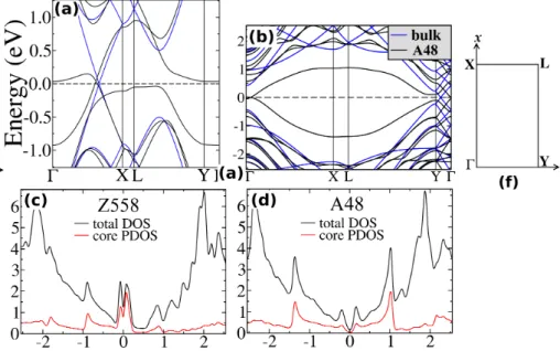
boron nitride as a function of the nitrogen chemical potential µN. The maximum and minimum values of µN are given in the text (see Eq. 2). Vertical lines indicate the values of µN for different molecular and solid-state sources of N-rich and B-rich environments. . . 25 4.8 Band structure and density of states (DOS) for the A48 and Z558 in
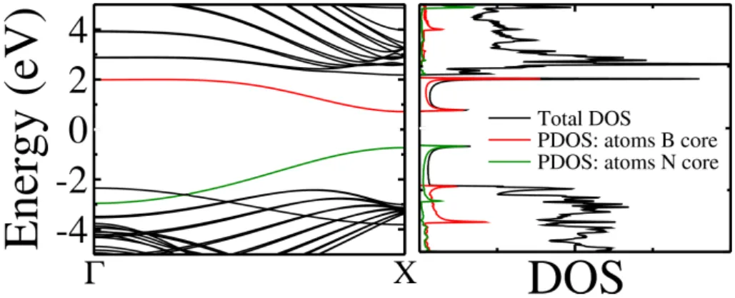
graphene. Black curves show the (a) Z558 and (b) A48 supercell band structure while the blue curves show bulk bands folded onto defect su-percell. (c) and (d) show total DOS and the projected DOS (PDOS) for the core atoms for the Z558 and A48, respectively. (f) The Brillouin zone corresponding to the supercell calculations in the present study. . . 29 4.9 Band structure and DOS for bulk BN and the AS48 boundary. The
4.10 DOS, PDOS, and band structures along the Γ-X line (parallel to the APB direction) for the ZB558 (top row) and ZN558 (bottom row). Supercell calculations are shown in the left panels and ribbon calculations in the right panels. The contribution of the core-atom orbitals to the total DOS is shown by green (N orbitals) and red (B orbitals) PDOS curves. Defect bands in the gap are shown by green and red curves, according to the dominant atomic-orbital contribution in each case. The DOS features associated to the ribbon-edge states are shown by orange curves in the right panels. . . 32 4.11 DOS, PDOS, and band structure along the Γ-X line (parallel to the APB
direction) for the ZN6 and ZB6 boundaries, from a supercell calculation. Defect bands in the gap and PDOS curves are shown by green (ZN6 states) and red (ZB6 states) curves, according to the dominant atomic-orbital contribution in each case. . . 33 4.12 DOS, PDOS, and band structures along the Γ-X line (parallel to the APB
direction) the ZCB558 (top row) and ZCN558 (bottom row) boundaries,
from a supercell calculation. Contributions of the core-atom orbitals to the total DOS are shown by blue (N orbitals), green (B orbitals), and red (C orbitals) PDOS curves. Defect bands in the gap are shown by green, red, and blue curves, according to the dominant atomic-orbital contribution in each case. . . 34 5.1 Electronic bands at the K point in the BZ for (a) graphene monolayer
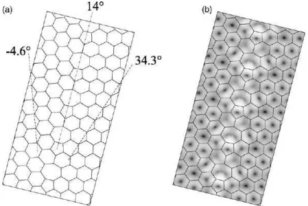
and (b) AB’ stacked graphene bilayer: the linear character of the bands in monolayer is lost with the introduction of the second layer, giving rise to doubled bands with parabolic dispersion around the Fermi level. . . 37 5.2 Moire pattern formed by relative rotations between graphene layers. For
different angles of rotation θ, a characteristic physics is observed in the electronic properties of this material. . . 37 5.3 Geometries of extended one-dimensional periodic defects in graphene,
in-vestigated in Ref.[31]; Introduction of GB(2,0)|(2,0) gives rise to magnetic states in graphene. Grain boundaries GB(5,0)|(3,3), GB(5,3)|(7,0) and GB(2,1)|(1,2), introduces electronic states which hybridize with the bulk states and are only partially confined to the defect core. . . 38 5.4 (a) The honeycomb structure of graphene monolayer in (a) and the two simplest
stackings between two layers: The AA’ stacking, in (b), where atoms of the same sublattice in the top and bottom layers are positioned directly above each other. The AB’ stacking, in (c), is formed when sublattice A in the top layer is placed directly above sublattice B’ in the bottom layer. . . 39 5.5 Geometries of one-dimensional periodic defects in graphene. In (a) the
trans-lational GB named GB(2,0)|(2,0) and the tilt GBs in (b) GB(1,2)|(2,1), (c) GB(5,0)|(3,3) and (d) GB(5,3)|(7,0). The translation vectors of the defect core
TGB, shown as a black arrow, can be written as a sum of the lattice vectors in
graphene bulk, in both sides of the grain boundary, and define the labels for the for different models considered.. . . 40 5.6 Optimized atomic model of the grain boundary with a linear chain of
5.7 Schematic suppercell for the defective bilayer graphene (left) and the correspond-ing Brillouin zone (BZ) (right). The high-symmetry lines are defined by the special points Γ, X, L and Y. Γ-Y and X-L lines are in the same direction of the GB for all models. . . 42 5.8 Electronic structure of the graphene monolayers with the tilt grain boundaries
GB(1,2)|(2,1), GB(5,0)|(3,3) and GB(5,3)|(7,0). The total DOS is represented by the black curves, while the red curves represent the partial DOS, projected onto the carbon atoms that form the defect core. . . 43 5.9 (a) Electronic bands and (b) DOS of the translational grain boundary GB(2,0)|(2,0)
in the graphene monolayer. The total DOS is shown by the black curve and the PDOS, projected onto the core atoms, by the red curve. In (a) is also included (in blue color) the band structure of a bulk suppercel obtained by removing the two atoms forming the dimer at the center of the defect core . . . 44 5.10 Graphene Bilayers constructed from the monolayers with grain boundaries
in-vestigated in Ref. [31]. A reasonable choice of initial structures is to define an AB’ stacking in some region, which consequently lead to the formation of Moire patterns in the region that presents a rotation due to the introduction of the GBs. 45 5.11 Unit cells for bilayer graphene with GB(5,3)|(7,0) defects with 336 and
422 atoms, with distance between GBd= 10.2 ˚A and 14.3 ˚A. The bottom pristine graphene layer is represented in gray, while the atoms in green represent the top layer, with two defect lines. The portion of the graphene lattice with armchair orientation along the GB direction is chosen to have an AB’ stacking registry with the additional second layer. . . 46 5.12 Unit cells for bilayer graphene with GB(2,0)|(2,0) formed by 168 and 254
carbon atoms with distances between adjacent GB of d = 14.4 ˚A and 23 ˚A, respectively. In this case, the introduction of three line defects is necessary to build the periodic structure composed of two layers, as the GB translate the lattice by 1/3 of the lattice period along the armchair direction (aAC vector defined in Chapter 2). . . 47 5.13 Electronic structure for monolayer (upper panel) and bilayer graphene
with supercells of two different sizes (middle and lower panels) with GB(5,0)|(3,3). A very similar electronic dispersion is observed for the three systems, with the main differences observed at the FL region. . . 48 5.14 Electronic structure for monolayer (top panel) and graphene bilayers
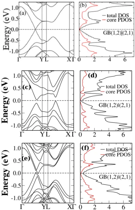
(middle and lower panels) for systems with GB(1,2)|(2,1). The distances between defect lines are d = 17.2 ˚A for the defective monolayer and d= 12.3 ˚A andd= 17.2 ˚A for the defective bilayers. . . 50 5.15 Electronic structure for defective bilayer graphene with GB(1,2)|(2,1) and
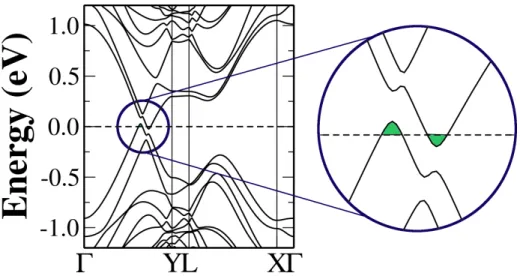
d = 17.2 ˚A. A semimetalic behavior is observed when a second pristine graphene layer in introduced in this system. . . 51 5.16 Electronic structure for monolayer (upper panel) and bilayer graphene
(middle and lower panels) with GB(5,3)|(7,0). For the three models, electronic states due to the defect are mixed with bulk states indicating a high degree of hybridization between such states. . . 53 5.17 Band structure and DOS of the translational GB(2,0)|(2,0) in monolayer graphene.
5.18 Electronic bands and DOS for the bilayer graphene with distance between trans-lational GB(2,0)|(2,0)d= 14˚A. (a) Calculation with no spin polarization shows a highly-localized peak at the FL, with a contribution of states from atoms that form the core of∼73%. (b) Spin polarization calculation stabilizes a magnetic state with magnetic moment 0.12µB (per defect unit). The main differences
be-tween total DOS of majority (black curve) and minority (blue curve) spin show up between -0.1 and 0.3 eV. . . 55 5.19 Electronic structure for GB(2,0)|(2,0) graphene bilayer, for the 254-atoms
supercell (d=23.0 ˚A). The neutral system in (a-b) does not present mag-netic moment. (c-d) By adding an extra charge, the FL is raised by 0.03 eV and a spin polarization calculation reveals a magnetic state with total DOS for majority and minority spins as represented black and blue colors, respectively in (e-f). . . 57 6.1 Band structure of bilayer graphene. Double parabolic bands are observed at low
energies with two of them (Ψ+
v and Ψ−c) touching at zero energies and the other
two (Ψ−
v and Ψ+c) showing an energy gap of 2γ(γ ≈0.35 eV). . . 63
6.2 Example of incidence from the k- to the q-region. Electron emerging from a state of positive energy ϕ+a(b) with angle of incidence θk can be transmitted to
theq-region for states Ψ±
c with transmission probabilities Tc± or reflected back
to theq-region. Angles θk(= arctan(ky/kx)), andα±c are also shown. . . 65
6.3 Interface between uncoupled layers, that obey the Dirac Hamiltonian of mono-layer graphene, and a region of bimono-layer graphene for which a parabolic dispersion is observed at low energies. . . 66 6.4 Scattering from k- to q-region: electrons initially in a region with linear
dis-persion (left panel), characteristic of monolayer graphene systems, go through a region of bilayer graphene with parabolic dispersion (right panel). . . 66 6.5 Critical energies occurs for initial states when it is not possible to conserve the ˆy
component of momentum in the scattering process. The yellow area in the blue circle corresponds to the range of initial momentumkin the k-region for which the ˆy component can be conserved in theq-region. For scattering from ak- to a
q-region we havekc =cos2γ(θk). . . 69
6.6 Reflection coefficients|ra|2,|rb|2andR=|ra|2+|rb|2for direct incidence (θk= 0)
from k- toq-region as a function of the energy of incidencek. . . 73 6.7 Transmission coefficients T+
c and Tc− to states of higher and lower energy in
bilayer graphene Ψ+
c and Ψ−c , and total transmission to theq-regionT =Tc++Tc−. 73
6.8 k-toq-region: Reflection coefficients|ra|,|rb|for layersaandband total reflection
|R| = |ra|+|rb|as a function of the angle of incidenceθk. . . 75
6.9 k-to q-region: Transmission coefficients T∓
c for statesP si∓c and total reflection
T =T−
c +Tc+ to theq-region as a function of the angle of incidenceθk. . . 75
6.10 For scattering from aq- to ak-region electrons at low energies go from a parabolic to a linear dispersion regime. . . 76 6.11 Interface between bilayer graphene and a second region of uncoupled graphene
layers. . . 76 6.12 For electrons crossing an interface between aq- and ak-region the critical angle
kc is defined askc=γtg2(α−c) for incidence from Ψ−c. . . 77
6.13 q- tok-region: Reflection coefficients as a function of the (a) incident energyk
and (b) angle of incidence α+
c for incidence from states of higher energy Ψ+c.
Reflection occurs just for the same state of incidence, so thatR =R+
6.14 q- to k-region: Transmission coefficients for incidence from Ψ+
c as a function of
the (a) incident energy k and (b-c) angle of incidence α+
c. For incidence from
Ψ+
c states, electrons are equally transmitted for both uncoupled layers and the
total transmission is T = 2×Ta(b). . . 80 6.15 q- to k-region: Reflection coefficients as a function of the (a) incident energy
k and (b) angle of incidence α−
c for incidence from states of lower energy Ψ−c.
Reflection occurs just for the same state of incidence, so that R = R−
c. The
regions of total reflection (R= 1) are defined by the critical energieskc=γtg2(α−c ). 81
6.16 q- to k-region: Transmission coefficients for incidence from Ψ−
c as a function of
the (a) incident energy k and (b-c) angle of incidence α−
c. For incidence from
Ψ−
c states, electrons are also equally transmitted for both uncoupled layers, so
that the total transmission isT = 2×Ta(b). Regions of null transmission (T = 0)
can be observed for energiesk < kc =γtg2(α−c). . . 81
6.17 Dispersion relations for q-k-q regions, that defines the barrier problem of two semi-infinite graphene bilayers separated by a finite region of two uncoupled monolayers.. . . 82 6.18 Transmission coefficients T+
c for incidence from Ψ+c state as a function of the
incident energy k, for the barrier widths (a) d=6 nm, (b) d=10 nm and (a)
d=13 nm.. . . 85 6.19 Transmission coefficients T+
c for incidence from Ψ+c state as a function of the
angle of incidenceα+
c, for the barrier widths (a)d= 6 nm, (b)d= 10 nm and (a)
d= 13 nm. . . 85 6.20 Transmission coefficients T−
c for incidence from Ψ−c state as a function of the
incident energy k, for the barrier widths (a) d=6 nm, (b) d=10 nm and (a)
d=13 nm.. . . 86 6.21 Transmission coefficients T−
c for incidence from Ψ−c state as a function of the
incident angle α−
c, for the barrier widths (a) d=6 nm, (b) d=10 nm and (a)
d=13 nm.. . . 87 7.1 STM imaging of atomically-sharp G|BN heterointerface. (a) BN nucleates
on the edges of graphene on Ru(0001) by a low dosage of borazine (5L) at 800 K. (b) A sharp G|BN interface with length <21 nm at 800 K. (c) Magnified view in b shows the formation of a seamless G|BN interface at the atomic scale. (d) Magnified view of (c) shows a zigzag edge of graphene bonded to a zigzag edge of BN at the interface. Scale bars in a-d are 50, 2.5, 0.5 and 0.25 nm, respectively. . . 92 7.2 Stretching in the C-N(B) bonds at the interface between h-BN and graphene
due to the mismatching of the lattices. . . 93 7.3 The formation of MDs at extended G|BN interface (>100nm). (a)
7.4 Strain profile of BN at G|BN interface with and without MD. (a), Il-lustrates the formation of MDs in layered heteroepitaxial growth of thin film above a critical thickness (tc). (b), For the graphene edge templated heterogrowth of BN, a misfit dislocation forms above the critical width (wc) to relieve strain. (c) Left: atomic resolved coherent lattice at the G|BN interface for strain analysis. Right: Experimental values of strain propagation parallel to the interface before (in red) and after (in blue) introducing MD. . . 96 7.5 Interfaces between h-BN and graphene formed by (a) C-B and (b) C-N bonds.
Nitrogen and boron atoms in h-BN are respresented in blue and green colors, while carbon atoms are shown in gray. The core MDs in the h-BN lattice formed by the pentagon-heptagon pair for each of these interfaces are also shown.. . . . 97 7.6 Example of a super-cell with C-N interface. In order to simulate the
graphene substrate, the two zigzag lines of carbon atoms at the edge of graphene side (in light blue box), are fixed during the optimization of the structure. The distance d of the 5-7 ring (in light green) from the interface (in light yellow) is chosen as that observed in the experiment, of ∼5 lattice parameter. . . 98 7.7 (a), Average strain profile for interfaces with (in blue color) and without
(in red color) MD for different lateral sizes of the nanoribbons. Ribbons with 11 and 15 lines of zigzag BN lines (nBN) where used for the models without MD, while ribbons with nBN = 13, 17 and 19 were used for the interfaces where we have included the MD. (b), A nanoribbon with MD, showing the numbering scheme for the zigzag BN lines [the horizontal axis in (a)] for which the average strain were computed. . . 99 7.8 Average strain profile for C-B (in green color) and C-N (in blue color)
zigzag linked interfaces compared to that of defect free interface (in red color). Both atomic configurations of the zigzag linked G|BN boundary (C-B and C-N) with the MD are equally efficient in relief the strain in the BN lattice. . . 101 7.9 Stone-Wales (left) and isolated pentagon-heptagon pair (right) introduced in
a hexagonal lattice. Both defects induce buckling in the planar sp2 bonded
structure as a mechanism of strain relief due to the compressed bonds. . . 102 7.10 Initial supercell with MD and the optimized structure: the pentagon-heptagon
pair induces the buckling of the heterostructure, and a reduction of the strain is observed. . . 103 7.11 High profiles in valleys with and without the dislocation core in BN-lattice.104 7.12 . . . 106 7.13 Probing the intrinsic electronic states at the G|BN interface after O2
7.14 Calculated electronic properties of G|BN heterostructures with linked C - N (higher panel) and C - B (lower panel) zigzag interfaces. Total density of states (DOS) and partial DOS (PDOS) analysis shows the introduction of interface states near the FL at ∼ 0.08 eV for C-N and ∼ -0.15 eV for C-B interfaces. States due to the 5-7 pair introduce a sharp peak at 0.8 eV and -0.63 eV, for C-N and C-B, respectively. . . 110 7.15 Local density of states (LDOS) for G|BN heterostructures with C-N (left) and
C-B (right) bonds at the interface. For each interface the LDOS is plotted for states in the energy range corresponding to the peaks in the DOS with major contribution from the atoms of the interface (0.05 to 0.15 eV for the C-N interface and -0.2 to 0.06 eV for the C-B interface). . . 111 7.16 Calculated electronic properties of G-BN heterostructures with linked
C-N (higher panel) and C-B (lower panel) zigzag interfaces including the edge states of both graphene and h-BN lattice. Edge states (in green and yellow) are strongly localized at the edges and can be discerned from the interface states. . . 113 8.1 Structural model for the orthorhombic cell of theα-phase. We show the unitcells
for single and double layers, which are repeated along the ˆx direction. A zoom in the structure shows one atomic species and its three first neighbors of the second atomic species that compounds the system. . . 117 8.2 (a) Unitcell and (b) the repeated structure of the bulk in the α phase. The
respective BZ is shown in (c) with the special points Γ, Y, T, Z, localized at theb∗-c∗, plane, corresponding to the plane of the puckered layers in the reals space. The orthorhombic lattice is shown in (d) . . . 118 8.3 Different types of interatomic distances for theαphase of SnS, SnSe, GeS, GeSe.
The small circles (M) stands for Sn and Ge, while the large circles (X) stands for Se and S atomic species. Figure taken from Ref. [126]. . . 120 8.4 Electronic band structures for single-layer, double-layer and bulk for α phase
of SnS. Indirect band gaps are calculated for all models, and direct band gaps higher in energy by a few meV define the possible direct transitions 1 and 2. The red and green points mark positions of CBM and VBM respectively. . . 122 8.5 Electronic band structures for single-layer, double-layer and bulk forαphase of
SnSe. A direct gap is predicted for single-layer, while indirect gaps are calculated for double-layer and bulk. The red and green points mark positions of CBM and VBM respectively. . . 124 8.6 Electronic band structures for single-layer, double-layer and bulk forαphase of
GeS. Indirect gaps are predicted for single-layer and double-layer, while a direct gap is calculated for the bulk. The red and green points mark positions of CBM and VBM respectively. . . 125 8.7 Electronic band structures for single-layer, double-layer and bulk forαphase of
4.1 Formation energies (Ef in eV/˚A), and average, maximum, minimum, and dispersion values for bond lengths (din ˚A) and bond angles (θ) for zigzag and armchair grain boundaries in graphene. . . 20 4.2 Edge energy per edge unitλedgef from fitting of triangle energies to Eq. 5,
for the N-rich zigzag edge (ZN-edge), and the B-rich zigzag edge (ZB-edge), for different values of N-rich and B-rich chemical potentials. . . 24 4.3 Comparison of formation energy values Ef of grain boundaries and
an-tiphase boundaries in monolayer BN computed with supercells and ribbon geometries. Supercells are stoichiometric and corresponding Ef values do not depend on chemical potentials of B and N. Supercells for non-stoichiometric boundaries contain the pair of partner boundaries indi-cated. In the top part of the Table, the sum of the Ef values obtained for the two boundaries using the ribbons is given for comparison with su-percell results. Values for the individual non-stoichiometric boundaries, computed with the ribbons, are given in the bottom part of the Table, for the limiting N-rich and B-rich environments.. . . 27 4.4 Formation energy of grain boundaries and antiphase boundaries in
mono-layer BN from combination of elastic energy and chemical-bond energy models. . . 27 7.1 Formation energy per unit length (eV/˚A) for C-B and C-N interfaces with
and without the MD for different values of N-rich and B-rich chemical po-tentials. Calculations of individual interfaces were obtained using ribbons. Results for two positions for the 5-7 ring from the interface (d1 = 0.65 nm
and d2 = 1.08 nm) are also included. . . 106
8.1 Optimized lattice vectors for αphase of SnS, SnSe, Ges, GeSe. . . 119 8.2 Ab initio interatomic distances according to Fig. 8.3. A1 stands for atomic
species Sn and Ge while A2represents S and Se. With the interatomic distances
type we denote in and ex as the distances valid for intra and inter puckered layers, respectively. The experimental values obtained in Ref. [126] are shown in parenthesis.. . . 120 8.3 Total energies (ET) and gap energies(Eg) for monolayer, bilayer and bulk of SnS,
SnSe, GeS, GeSe. The star (*) indicates the direct band gaps. . . 121 8.4 Direct transitions energies observed from band structure calculations for all
com-pounds, indicated by blue arrows in Figs. 8.4, 8.5, 8.6 and 8.7. These transitions are higher in energy by a few eV than the energy gaps. . . 123
Introduction
Two-dimensional (2D) materials have been an extensively studied classes of materials since a single-layer graphene was obtained in a stable form by mechanical exfoliation[1].
From there, the interest in 2D crystals was promptly extended to matherials other than graphene, such as hexagonal boron nitride (h-BN) and layered metal dichalcogenides
(LMDCs) to name a few[2–4].
The development of reliable synthesis methods of single and few-layer 2D materials
combined with their unusual and very interesting properties, directly related to their lower dimensionality, has attracted a massive attention of the scientific and industrial community. Much progress has been made, but it is still a challenge to obtain a total
control of the properties of any material at the nanoscale.
The synthesis process of materials in this scale results in polycristalline samples with
abundant topological defects. A great improvement in the production of defect-free low dimensional materials has been made[5, 6], but defective samples are very com-monly obtained. Introduction of defects strongly influence the electronic, chemical, and mechanical properties of materials, and a deep understanding on how these properties are altered in the presence of different defects is of essential importance to achieve the
desired control of these properties.
In this thesis we use first principles calculations based on the formalism of Density
Functional Theory (DFT) to investigate electronic and structural properties of two-dimensional materials. Defective graphene and hexagonal boron nitride are the main
focus, while preliminary results of a work in progress are also presented, were we inves-tigate two-dimensional monochalcogenide semiconductors.
The thesis is organized as follows:
In the Chapter 2, we provide a brief overview of basic concepts on graphene and boron nitride.
In the Chapter 3 we present the methodology used for the development of the
work.
In the Chapter 4, we present a study of stability and electronic properties of
nine different models for extended one-dimensional (1D) defects in monolayer BN.
A low-energy stoichiometric model for an armchair-direction antiphase boundary (APB) in monolayer BN is introduced.
In the Chapter 5, grain boundaries in graphene bilayers are investigated, aiming
at the understanding of the degree of localization of the electronic states in the atoms that compose the core of the line defects. Interesting results like magnetic
instabilities and changes from metallic to semi-metallic character of these systems are discussed.
In the third work, presented in Chapter 6, we study the low-energy electronic
transport across stacking boundaries in graphene. The electron scattering by in-terfaces formed between regions of monolayer and bilayer graphene is investigated
by a continuum approach.
In the Chapter7, we discuss a work that was developed in collaboration with an
experimental group of the Graphene Research Centre (GRC) of the National Uni-versity of Singapore (NUS) and with Prof. Antˆonio H´elio Castro Neto. Results
obtained from synthesis of coherent interfaces between graphene and h-BN moti-vated DFT calculations to investigate the introduction of a core dislocation in the h-BN lattice as a mechanism of strain relief, in order to keep the continuity of the
film along the interface. Electronic properties of this system are also discussed.
In the Chaper8, preliminary results of a study of two-dimensional semiconductors
monochacogenides is presented. It focuses on the electronic and optical properties
Two-Dimensional Materials: A
brief introduction to Graphene
and hexagonal-Boron Nitride.
2.1
Graphene structure and electronic dispersion.
2.1.1 Single layer graphene.
The hexagonal structure of graphene, with two carbon atoms per unit cell, can be seen as made out of two interpenetrating triangular lattices as presented in Fig.2.1-a. With the value of the carbon-carbon distance a = 1.42 ˚A obtained experimentally[7], the lattice vectors can be written:
a1 =
a
2(3, √
3), a2=
a
2(3,− √
3), (2.1)
with the three nearest-neighbor vectors~δ1,~δ2 and~δ3 given by:
δ1 =
a
2(1, √
3), δ2 =
a
2(1,− √
3), δ3 =−a(1,0) (2.2)
as shown in Fig. 2.2.
In addition to the aforementioned lattice vectors a1 and a2 usually adopted to describe the structure of graphene, we define the vector aac as shown in Fig. 2.2, which define the lattice period along the armchair direction of graphene.
Figure 2.1: (a) Honeycomb lattice of graphene formed by two interpenetrating
tri-angular lattices named A (atoms in red) and B (atoms in gray) lattices. The lattice vectors~a1 and~a2 are also shown. (b) Brillouin Zone defined by the reciprocal lattice
vectors~b1 and~b2 and the position of the special Dirac points K and K’, around which
the electronic dispersion is linear for low energies.
Figure 2.2: The unitcell of graphene highlighted by the yellow box and the
transla-tional vectoraacthat defines the period along the armchair directions of the hexagonal
By the definition of reciprocal space vectors, bi = 2π~ai·~a(j~a×j×~ak~a
k), the reciprocal vectors
for this triangular lattice are given by:
b1 = 2π
3a(1,
√
3), b2 = 2π
3a(1,−
√
3). (2.3)
The two-dimensional Brillouin Zone (BZ) of graphene, defined byb1 andb2, has also a
hexagonal form, but rotated by 30° in relation to the lattice in the real space, as seen
in Fig. 2.1-b.
The main electronic properties of graphene are well documented in the literature, with a massive number of works on this topic, since it became the “material of the future”.
The tight-binding approach has been largely used to describe its electronic dispersion, as an analytic expression for the energy bands can be obtained in a reasonable accordance with more accurate results.
The energy bands derived from a tight-binding Hamiltonian were first derived by P. R. Wallace [8], and have the form:
E±(k) =±tp3 +f(k)−t′f(k), (2.4)
with
f(k) = 2cos√3kya
+ 4cos
√ 3 2 kya
!
cos
3 2kxa
. (2.5)
Here, t ≈ 2.8 eV is the nearest-neighbor hopping energy (hopping between different sublattices), and t′, the next nearest-neighbor hopping energy.
By expanding the full band structure in Eq.2.4 around to the K~ (K~′) vectors, which
define the K (K’) points in the BZ, as k= K~ +q, with |q| ≪ |K~|, we have, for the π
bands:
E±(q) =±~νF|q|+O[(q/K)2], (2.6)
whereνF is the Fermi velocity, given byνF = 3ta/(2~) ≃1×10⁶m/s. The linear energy
dispersion close to theK (K’) points, is characteristic of massless Dirac fermions.
Figure 2.3: Electronic dispersion for the honeycomb lattice of graphene. The Dirac
points localized at the six corners of the hexagon that define the BZ show linear dis-persion at low energies.
2.1.2 Bilayer graphene: AB’ and AA’ stackings.
The simplest realization of a multilayer graphene system is that formed by two layers pilling up together in the known Bernal or AB’ stacking. As shown in Fig. 2.4, the Bernal stacking is defined when different sublattices of the two graphene layers are positioned directly above each other. So, if a sublattice A of a ‘top’ graphene layer is positioned above the sublattice B’ of a ‘bottom’ graphene layer, where we use the prime
to distinguish the two layers, this stacking is of the AB’ type, as shown in Fig. 2.4. In the same way, if the same sublattices from both layers are positioned directly above each
other, we have an AA’ stacking. Such definitions will be used throughout this work.
The two layers in a graphene bilayer system are weakly coupled by van der Waals
forces[7], and the measured interlayer distance is ∼3.4˚A.
The tight-binding model developed for graphene and briefly presented here, can be
extended to stacks with a finite number of graphene layers. The first approximation for this problem is to consider the inclusion of the hopping energy between nearest-atoms belonging to different layers, γ. For AB’ stacking, γ is the hopping energy between the
atoms of sublattices A and B’ of the two layers.
For free electrons in a bilayer graphene with AB’ stacking, the solution of the eigenvalue
problem gives a parabolic relation between low energy states and total momentum q=
p
Figure 2.4: (a) AA’ and AB’ stackings in bilayer graphene. The AB’ stacking is
defined whit the A sub-lattice (in red) of the top layer positioned directly above the B’ sub-lattice (in gray) of the bottom layer. In a similar way, a AA’ stacking is defined
when the top A(B) sub-lattice is directly above the bottom A’(B’) sub-lattice.
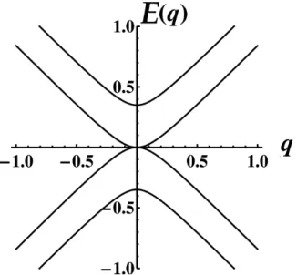
Figure 2.5: Parabolic electronic dispersion for bilayer graphene in the AB’ stacking.
E(q) =±γ±
p
4q2+γ2
ht
Figure 2.6: h-BN lattice adopts the same structure as in graphene but is formed by
different atomic species: B and N. The unit cell is shown by the yellow box.
2.2
Hexagonal Boron Nitride.
Despite adopting exactly the same hexagonal structure as graphene, hexagonal boron nitride (h-BN) shows a completely different electronic behavior, due to the asymmetry
between the two sublattices, that are now occupied by different atomic species. By con-sidering a minimal tight-binding model for a single layer h-BN, that takes into account
the hopping t among nearest neighbor atoms and on-site energies for boron (EB) and
nitrogen (EN) atoms, it can be shown[9] that the energy relation dispersion assumes the
form:
E(k) =E0± 1 2
q E2
g + 4|φ|2 (2.8)
where it can be identified the insulating behavior of this material, with energy gap
Eg =EB−EN >5 eV[9,10]. We also have in Eq.2.8E0 = (EB+EN)/2 the energy in
the middle of the gap and
φ/t= 1 +eia(−kx/2+
√
3ky/2)+eia(kx/2+
√
3ky/2). (2.9)
In this way the Dirac cones observed in graphene do not appear in h-BN due to the
Methodology
3.1
Density Functional Theory
In quantum mechanics, all information about a given system is contained on its wave function, that can be obtained by solving the Schr¨odinger equation (SE). So, in
prin-ciple, if we know the wave function of a given system we can extract from it all other information of interest.
In this way, the starting point to solve a quantum system is the resolution of its Schr¨odinger equation, that for a generic electronic system with N electrons can be
written:
HΨ(~r1, ~r2, ..., ~rN) =EΨ(~r1, ~r2, ..., ~rN). (3.1)
However, resolution of such equation presents a great challenge. The exact solution of
3.1can be obtained analytically just for the hydrogen atom (N=1); for a system with 2 electrons, it is already required the use of approximations to describe electron- electron
interactions. For a simple system with about 10 electrons (a CH4molecule, for example), we are already facing a huge problem, which solution is quite difficult even with more
sophisticated computational methods [11].
DFT is an alternative to solve the electronic Hamiltonian of many-body systems. The idea is to promote the particle density ρ(~r) to the status of key variable, on which the
calculation of all other observables can be based.
The advantage of this choice is that now we are dealing with a function of just three
variables, the three spacial coordinates of ρ(~r), that is more practical than the wave function, with 3N variables.
3.1.1 Hohenberg-Kohn Theorems
The Hohenberg-Kohn theorems [12] states that ρ(~r) can be used in a many-body elec-tronic system as the key variable, of which all observables are functionals. The first
Hohenberg-Kohn theorem states that:
The external potentialν(~r), and hence the total energy, is a unique functional of the electron density.
So, ρ(~r) would be sufficient to know Ψ(r~1, ..., ~rN) from which we could obtain all
rel-evant informations in our problem. From this, we conclude that the wave function
Ψ(r~1, ..., ~rN) is a functional of the density ρ(~r), and as all observables can be obtained
from Ψ(r~1, ..., ~rN), they can also be written as functionals ofρ(~r). In special, the ground
state energyE0 can be expressed in terms of the ground-state densityρ0(~r):
E0 =minE[ρ] =hΨ[ρ0]|H|Ψ[ρ0]i. (3.2)
The energy functional presents the variational property
E[ρ0]≤E[ρ] (3.3)
whereρ0 is the ground-state density, and ρis some other density. Equation (3.3) tell us that the calculation of the energy by a different density than the ground-state density,
give us an energy higher than the ground-state energy. This important information is known as the second Hohenberg-Kohn theorem:
The ground state energy can be obtained variationally: the density that min-imizes the total energy is the exact ground state density.
Despite the great importance of the Hohenberg-Kohn theorems, which allow us to express
any physical observable as unique functionals of the electronic density, effectively to solve the many-body problem requires a more practical scheme than the earlier attempts of
minimizing E as a functional ofρ directly.
The Kohn-Sham approach, presented by Kohn and Sham [13] in the form of the called Kohn-Sham equations, is nowadays the most common and efficient way of minimizing
3.1.2 Kohn-Sham equations
In the Kohn-Sham formulation, it is possible to solve the total energy functional almost
exactly, remaining only a small part to be solved approximately.
The total energy functional of a generic system can be decomposed as:
E[ρ] =Ts[ρ] +Tc[ρ]
| {z }
Te[ρ]
+UH[ρ] +Uxc[ρ]
| {z }
Vee[ρ]
+Uext[ρ]. (3.4)
Here, Ts[ρ] is the single particle kinetic energy, that represents the kinetic energy of
a non-interacting electron system with density ρ;Tc[ρ] is the kinetic energy correlation
term, due to the electron interactions effects. The electron- electron interaction potential
Vee[ρ], is dismembered in a classical contribution, the Hartree energy UH[ρ], and in a
part of quantum nature Uxc[ρ], which includes exchange and correlation effects. The
remaining term Uext[ρ], represents the potential due to the external sources.
The explicit form of Ts[ρ],Uext[ρ] and UH[ρ] can be written:
Ts=−1
2
N X
i=1
Z
φ∗i(~r)∇2φi(~r)d~r (3.5)
UH[ρ] =
1 2
Z Z ρ(~r)ρ(~r′)
|~r−~r′| d~rd~r′ (3.6)
Uext[ρ] = Z
ρ(~r)νext[ρ]d~r (3.7)
with φi the single particle orbital, and νext the external potential per particle, which
depends on the interaction of the electronic system with external sources.
Despite of the fact that the explicit form of the remaining terms is not known, the Hohenberg-Kohn theorems ensure that they can be written as a density functional. It
is usual to join these unknown terms in one, the so-called exchange-correlation energy
Exc=Exc[ρ].
With these informations, we can rewrite Eq.3.4 as:
E[ρ] =Ts[ρ] +
1 2
Z Z ρ(~r)ρ(~r′)
|~r−~r′| d~rd~r′+
Z
In order to find expressions that allow us to obtain the total energy of the system, as well as another relevant properties, we proceed by minimizing the energy functional relative
to the electronic density ρ(~r). In their formulation, Kohn and Sham assume that the ground state density of the original interacting system ρ0(~r) is equal to that of some
chosen non-interacting system ρso(~r) :
ρ0(~r)≡ρs0(~r) =
N X
i
φ∗i(~r)φi(~r). (3.9)
From this derivation considerations, we get the expressions:
"
−12∇2+ 1 2
Z ρ(~r)
|~r−~r′|d~r+Uext[ρ] +
δExc[ρ] δρ
!#
φi(~r) =εiφi(~r) (3.10)
or
−12∇2+νef f(~r)
φi(~r) =εiφi(~r) (3.11)
where we consider the terms in parentheses as a unique effective potential νef f
νef f =
1 2
Z ρ(~r)
|~r−~r′|d~r+νext[ρ] +
δExc[ρ]
δρ . (3.12)
Equation 3.11 has the form of a single-particle Schr¨oedinger equation , and the single-particle orbitals φi(~r) provide the electronic ground state density of the non-interacting
systemρs
0(~r), that is the same as the one for the interacting system ρ0(~r).
The Kohn-Sham ansatz for the density (Eq. 3.9) make it possible to replace the many-body interacting problem by an auxiliary single-many-body system, which can be solved more easily.
In Kohn-Sham formulation, DFT looks formally like a single-particle theory, thought many-body effects are still included via the so called exchange-correlation functional.
3.2
Exchange-Correlation functional approximations
There are several different approaches used for the exchange-correlation potential,
In the LDA approximation, the real inhomogeneous system is decomposed in small cells on which the density ρ(~r) is approximately constant. If we consider, for each cell (i.e.,
locally), the per-volume energy (ehomxc ) of a homogeneous system to be approximately the contribution of each cell to the real inhomogeneous system, we can make these cells
infinitesimally small and sum over all cells to obtain:
Exc[ρ]≈ExcLDA[ρ] = Z
ehomxc [ρ(~r)]d3r. (3.13)
The functional ehomxc is decomposed in a contribution of the exchange and correlation
energies so thatehomxc =ehomx +ehomc . For the exchange energy, the per-volume energy is considered as that of the homogeneous electron liquid [14,15]. On the other hand, the correlation partehom
c is not known exactly, and approximations for this term are based
on parametrization of results obtained from Quantum Monte Carlo (QMC) calculations for the electron liquid[16].
Although the local approximation has proved quite successful, the real systems, such as atoms, molecules and solids, are all inhomogeneous, that is, their density ρ(~r) varies
spatially. An improvement of the LDA approximation is to consider the spatial varia-tion of the density in terms of the gradient ∇ρ(~r) in writing the exchange-correlation
functional Exc[ρ]. In this way, Exc[ρ] has the general form:
ExcGGA[ρ] =
Z
f(ρ(~r),∇ρ(~r))d~r (3.14)
and have become known as the generalized-gradient approximations (GGAs)[17].
Many different GGAs can be obtained, depending on the method of construction
em-ployed for obtainingf(ρ(~r),∇ρ(~r)). In physics, the most popular GGAs functionals are that proposed by Perdew, Burke and Ernzerhof (PBE)[18]. The BLYP, which denotes a combination of Becke’s exchange functional[19] and the correction functional of Lee,
Yang and Parr[20] are mainly used in chemistry.
Both GGA and LDA functional are very useful and have shown to produce reliable
3.3
The SIESTA and Quantum Espresso codes and the
main parameters considered in the calculations.
Except for Chapter 6, where continuum approach for the Dirac Hamiltonian was used to study interfaces between graphene layers, in all other works we employ a first prin-ciples approach based on the Kohn-Sham density functional theory (KS-DFT), [13], as
implemented in the SIESTA [22] (Chapters4, 5.10 and 7) and Quantum Espresso [23] (Chapter8) codes.
For works developed with SIESTA code, the generalized-gradient approximation (GGA) is used for the exchange-correlation term. [18] Interactions between valence electrons
and ionic cores are described by Troullier-Martins pseudopotentials. [24] and a double-ζ
pseudoatomic basis set augmented with polarization orbitals is employed, with an energy
cutoff of 0.01 Ry. From previous work by ours and other groups, it is established that this is a carefully-tested calculation setup for problems involving BN and carbon systems. Careful convergence tests of all our results were performed with respect to the numerical
parameters of these methodology. Structural optimization has been performed initially with residual forces of less than 0.04 eV/˚A on each atom, and further relaxation of the
geometries has been carried out with a more stringent tolerance of 0.005 eV/˚A. Values of 200 Ry and 250 Ry for the equivalent plane-wave cutoff for the real-space integration
mesh have been used for total energy calculations and geometry relaxations.
In Chapter8the DFT calculations are performed using the plane-wave pseudopotential method[25, 26] as implemented within the QUANTUM-ESPRESSO package. Norm-conserving pseudopotentials for Sn, Ge, Se and S are generated with the APE pseu-dopotential generator. For all calculations the wave functions are expanded in plane
waves with a kinetic energy cutoff of 70 Ry. This value has been shown enough for energy convergence, as some earlier works[27] used for very similar systems a cutoff of 50 Ry, that already reproduces well converged results. Structural optimization was
Stability of edges and extended
defects on boron nitride and
graphene monolayers: the role of
chemical environment
4.1
Introduction
Many proposed applications of nanomaterials require the ability to control their
elec-tronic properties. In particular, graphene and boron nitride (BN) in the two-dimensional (2D) monolayer form have become an important subject of research, owing to their me-chanical strength and a rich variety of physical phenomena connected to their electronic
structure. [7] The introduction of structural defects presents an alternative for manipu-lating the electronic and magnetic properties in these materials. [7,28–33] In graphene grown on Ni(111) substrates, a translational grain boundary (GB) with a core structure
consisting of topological defects (TD) in the form of non-hexagonal rings (pentagons and octagons) has been theoretically proposed [29] and recently observed in STM
ex-periments by Lahiriet. all[30]. One of the images obtained in this experimental work is shown in Fig.4.1, where we can easily identify the GB formed by two pentagons followed by one octagon.
The occurrence of magnetism for the quasi-one-dimensional electronic states introduced
by this defect has also been suggested by ab initio calculations. [31] This graphene GB lies on the zigzag direction and arises due to the presence of two possible stackings of the graphene monolayer with respect to the Ni(111) substrate, which leads to the possibility
Figure 4.1: Scanning tunneling microscopy image of graphene on Ni(111) and the
superimposed defect model obtained in the experimental work in Ref. [30].
of domains related by a relative translation, with the GB emerging as the boundary between two such domains. [30] In the case of monolayer BN grown on Ni(111), the same
stacking mechanism holds, [34] and the possibility of engineering smaller band gaps in this large-band-gap material by the introduction of this zigzag-direction boundary has been recently considered. [32]
In this work, we introduce a low-energy stoichiometric model for an armchair-direction antiphase boundary (APB) in monolayer BN, [35] based on a structural pattern observed
experimentally in irradiated graphene in the form of finite segments of squares and oc-tagons. [36] A very recent experimental work [37], published after we finish our work
presented in this chapter, also shows that extended one-dimensional lines formed by a se-quence of square-octagon polygons can form in the hexagonal lattice of BN monolayers.
The origin of this defect occurs by a reconstruction process after electron bean irradia-tion, and the obtained structure can be identified by transmission electron microscopy and computational simulations, as shown in Fig.4.2-b and c.
Furthermore, we investigate the electronic properties and compare the stability of the aforementioned zigzag and armchair boundaries in graphene, as well as of nine different
models for extended one-dimensional (1D) defects in monolayer BN, including five vari-ations of the zigzag boundary with TDs in the core. The two graphene boundaries are
shown in Fig.4.3, and the nine BN boundaries are shown in Fig. 4.4.
This work was published in The Journal of Physical Chemistry C. Reference: L. C.
Figure 4.2: Transmission electron microscopy image for the finite segment of squares
and octagons obtained by electron bean irradiation in graphene in Ref.[36] in shown in (a). By the same process, this defect configuration was also obtained in the form of extended defect lines in BN [37]. In this case, TEM image is shown in (b), with the
atomic theoretical model (left panel) and corresponding simulated image in (c).
4.2
GB Models
The translational GB observed in graphene in Ref.[30] is obtained by cutting a graphene sheet along the zigzag direction, displacing the two halves by one-third of the lattice
period in the direction perpendicular to the cut, and inserting carbon dimers with their common bond oriented along the cut, generating a line of pentagon-pentagon-octagon units, as shown in the right panel in Fig.4.3. Being oriented along the zigzag direction, this boundary is labeled Z558 in our discussion. We also examine the armchair-direction counterpart of the Z558 in graphene. This armchair grain boundary, which we label A48,
can be obtained by cutting a graphene sheet in the armchair direction and translating one side of the sheet with respect to the other side by half the lattice period along
the armchair direction, generating a line defect that contains squares and octagons alternately arranged in its core, as shown in the left panel in Fig. 4.3. Small finite segments of this core structure have already been observed in graphene as result of reconstruction after electronic-beam irradiation. [36] Chiral GB geometries may also be built by combining these two basic structures.
Figure 4.3: Structures of grain boundaries (GB) in monolayer graphene. Left - A48:
an armchair-chirality graphene GB with fourfold and eightfold rings in the defect core. Right - Z558: a zigzag-chirality graphene GB with fivefold and eightfold rings in the
defect core. Core atoms are drawn as darker circles.
Figure 4.4: Structures of antiphase boundaries (APB) in monolayer boron nitride.
Boron, nitrogen, and carbon atoms are shown by orange, green, and grey circles, re-spectively. Labeling is explained in the text. Top row shows stoichiometric boundaries. Left panel - AS48: armchair chirality with a fourfold and an eightfold ring in the peri-odic unit of the defect core; [38] middle panel - AS6: armchair chirality with a hexagon in the core; right panel - ZS558 (a GB, not an APB): zigzag chirality with two pen-tagons and an octagon in the core. Middle row shows nitrogen-rich boundaries. Left panel - ZN558: zigzag chirality with two pentagons and an octagon in the core; middle panel - ZN6: zigzag chirality with a hexagon in the core; right panel - ZCB558: zigzag
chirality with two pentagons and an octagon in the carbon-doped core. Bottom row shows boron-rich boundaries. Left panel - ZB558: zigzag chirality with two pentagons and an octagon in the core; middle panel - ZB6: zigzag chirality with a hexagon in the core; right panel - ZCN558: zigzag chirality with two pentagons and an octagon in the
formed at the interface of two domains with opposite assignments of the B and N atoms to the two triangular sublattices of the BN honeycomb lattice. In this material, the
geometries of the graphene Z558 and A48 translate naturally into APBs. In the present study, we consider a total of eight APB models and one translational GB model in
BN. [32] The labeling we adopt for the line defects in BN is based on three features: (i) the chirality of the defect, with armchair(zigzag)-oriented defects denoted by the
letter A(Z); (ii) the stoichiometry (i.e., the number of B and N atoms) of the defect core, with stoichiometric cores indicated by the letter S, and boron(nitrogen)-rich cores indicated by the letter B(N); (iii) the types and multiplicities of the polygons present in
the periodic unit of the defect core, with each core polygon denoted by the number of its sides.
Hence, the two armchair-oriented stoichiometric APBs, shown in the left and middle panels in the top row in Fig.4.4are labeled AS48 and AS6, respectively, while the zigzag-oriented stoichiometric grain boundary (not an APB in this case) in the right panel is labeled ZS558. Generally, the core of zigzag APBs containing odd-membered TDs is either N-rich or B-rich, if one adopts the criterion of minimizing the number of homopolar
(N-N or B-B) bonds. We consider two N-rich versions of zigzag boundaries, shown in the middle row on the left and middle panels, labeled ZN558 and ZN6, respectively,
with the B-rich ZB558 and ZB6 counterparts shown in the bottom panel. Note that the ZN6 and ZB6 boundaries contain only hexagons in their core. [32] By replacing the B2 and N2 dimers with substitutional C2 dimers in the cores of the ZB558 and ZN558,
we obtain the carbon-doped ZCB558 (N-rich) and ZCN558 (B-rich) boundaries shown in the right panels of the middle and bottom rows, respectively.
To address all these models, we use supercells that are periodic in the monolayer plane. Very large vacuum regions (∼30-40 ˚A) are included to impose periodic boundary
condi-tions in the perpendicular direction. We have tested convergence of the structural and electronic properties, as well as of the energetics of the defects, by performing
calcu-lations with supercells where distances between the defects and their nearest periodic images in the monolayer plane vary between 10 ˚A and 19 ˚A.
4.3
Energetics
4.3.1 Defective Graphene
We seek to compare the relative stability of the above 1D defects in graphene and BN.
by
EfGB = E
GB
tot (N)−N µbulkgraph
ℓ (4.1)
where Edeftot (N) is the total energy of theN-atom supercell containing a GB, µbulk graph
=-154.867 eV is the bulk chemical potential of graphene, obtained as the total energy per atom in a pristine graphene calculation, and ℓ is the length of the supercell along the defect direction.
Our calculated values for EfZ558 and EfA48 in graphene are included in Tab. 1. In this material, the Z558 is more stable than the A48 by 0.25 eV/˚A due to the smaller bond-length and bond-angle distortions from the ideal bulk values (dbulk = 1.442 ˚A and
θbulk = 120◦ in our calculations) incurred in the pentagon-pentagon-octagon core of the
Z558, when compared with the tetragon-octagon core of the A48. Average bond lengths
and bond angles, as well as maximum and minimum values and standard deviations for these quantities are included in Tab. 1 for the Z558 and the A48. While average values
are similar for both bond lengths and bond angles, deviations from the bulk reference values are larger in the A48 core.
This indicates that the nature of the energy difference between the A48 and the Z558
in graphene is essentially elastic. Indeed, a Keating-model calculation with a Keating potential fitted for diamond carbon [39] predicts the elastic energy of the A48 to be about twice that of the Z558, in qualitative agreement with our ab initio results. A
more quantitative agreement would require fitting the Keating potential to the graphene bonding environment.
Ef d¯ dmax dmin σd θ¯ θmax θmin σθ
Z558 0.48 1.45 1.48 1.41 0.02 120◦ 141.7◦ 104.6◦ 11.1◦
A48 0.73 1.44 1.52 1.40 0.04 120◦ 147.9◦ 90◦ 16.8◦
Table 4.1: Formation energies (Ef in eV/˚A), and average, maximum, minimum, and
dispersion values for bond lengths (din ˚A) and bond angles (θ) for zigzag and armchair grain boundaries in graphene.
4.3.2 Defective BN.
In BN, the lack of inversion symmetry means that in a periodic supercell calculation for non-stoichiometric boundaries, such as the ZN558 and its ZB558 partner [and the
(ZN6,ZB6) and (ZCB558,ZCN558) pairs as well, both boundaries are included in the periodic cell, hence only the sum of the formation energies of the two 1D defects can be extracted from such calculation. Formation energies of individual boundaries can be