DEPARTAMENTO DE F´ISICA
PROGRAMA DE P ´OS-GRADUAC¸ ˜AO EM F´ISICA
FRANCISCO WELLERY NUNES SILVA
STRUCTURAL, ELECTRONIC AND TRANSPORT PROPERTIES OF NANOSCALED SYSTEMS
STRUCTURAL, ELECTRONIC AND TRANSPORT PROPERTIES OF NANOSCALED SYSTEMS
Tese de Doutorado apresentada ao Programa de P´os-Gradua¸c˜ao em F´ısica da Universidade Federal do Cear´a, como requisito parcial para a obten¸c˜ao do T´ıtulo de Doutor em F´ısica.
´
Area de Concentra¸c˜ao: F´ısica da Mat´eria Condensada.
Orientador: Prof. Dr. Eduardo Bedˆe Barros
STRUCTURAL, ELECTRONIC AND TRANSPORT PROPERTIES OF NANOSCALED SYSTEMS
Tese de Doutorado apresentada ao Programa de P´os-Gradua¸c˜ao em F´ısica da Universidade Federal do Cear´a, como requisito parcial para a obten¸c˜ao do T´ıtulo de Doutor em F´ısica.
´
Area de Concentra¸c˜ao: F´ısica da Mat´eria Condensada.
Aprovada em 26/08/2016.
BANCA EXAMINADORA
Prof. Dr. Eduardo Bedˆe Barros (Orientador) Universidade Federal do Cear´a (UFC)
Prof. Dr. Andrey Chaves Universidade Federal do Cear´a (UFC)
Prof. Dr. Jo˜ao Milton Pereira Junior Universidade Federal do Cear´a (UFC)
Prof. Dr. Eduardo Costa Gir˜ao Universidade Federal do Piau´ı (UFPI)
Biblioteca Universit´aria
Gerada automaticamente pelo m´odulo Catalog, mediante os dados fornecidos pelo(a) autor(a)
S58s Silva, Francisco Wellery Nunes .
Structural, Electronic and Transport Properties of NanoScaled Systems / Fran-cisco Wellery Nunes Silva. – 2016.
94 f. : il. color.
Tese (doutorado) - Universidade Federal do Cear´a, Centro de Ciˆencias, Pro-grama de P´os-Gradua¸c˜ao em F´ısica, Fortaleza, 2016.
Orienta¸c˜ao: Prof. Dr. Eduardo Bedˆe Barros
1. DFT. 2. Electronic Structure. 3. Graphene. 4. nanoribbon. 5. MoS2. I. T´ıtulo.
of science, and not merely a petty experimentalist, I should advise you to
apply to every branch of natural philosophy, including
I thank mom and dad...
I thank professor Eduardo Bedˆe Barros, for all his patience and advices given to me over the last years.
I thank Dr. Eduardo Cruz-Silva, for all his time and patience, during the time in which we worked together at PSU.
I thank professor Mauricio Terrones, for allowing me to join his group and helping me during my time at PSU.
I thank professor Humberto Terrones for every orientation and advices along all this time.
I thank professor Antˆonio Gomes de Souza Filho, for all support and compre-hension and for all advices and orientations as well along my journey at UFC.
I thank ”shihan” Josu´e Mendes Filho, for a life dedicated to this department, and for every thing which I have learned just observing him, who is a truthful master.
I thank professor Alexandre Ara´ujo Costa, who gave me indispensable support in a crucial moment of this step.
I thank Dr. Peter Koval for all good conversations about the SIESTA method.
I thank Dr. Andrei Postnikov for every tool shared for him, and for precious advices about the SIESTA method.
I thank professor Eduardo Costa Gir˜ao, for allowing our group to use his trans-port program.
I thank my room mates, Rafael, Bruno and of course Bruno ”senpai”, for every happy moment which came from a joke.
I thank Centro Nacional de Super Computa¸c˜ao CESUP, for every computa-tional support.
I thank Centro Nacional de Processamento de Alto Desempenho em S˜ao Paulo, for computational support.
M´etodos para c´alculos de estrutura de banda s˜ao aplicados neste trabalho, a fim de es-tudar as propriedades eletrˆonicas e de transporte de sistemas em nanoescala. A teoria do funcional da densidade (DFT) foi empregada para estudar as propriedades eletrˆonicas de uma ilha hexagonal de nitreto de boro (h-BN) embutida em nanofitas de grafeno (GNRs), considerando ambas as quiralidades de bordas, zigzag e armchair. Al´em disso, a contribui¸c˜ao do spin foi levada em conta no nosso c´alculo eletrˆonico. Os resultados referentes aos sistems n˜ao dopados mostraram a existˆencia de uma polariza¸c˜ao de spin natural associado a sistemas de borda zigzag, enquanto os sistemas de borda armchair s˜ao encontrados com spin degenerados no estado fundamental. N´os tamb´em investig-amos os efeitos devido `a dopagem com carbono no anel mais interno de um cluster de h-BN, onde o ´atomo C toma o lugar de um ´atomo de Boro ou de um ´atomo de Ni-trogˆenio. A dopagem conduz a uma estrutura de bandas ainda mais polarizada, para energias pr´oximas ao n´ıvel de Fermi. As propriedades de transporte eletrˆonico foram es-tudadas aplicando o formalismo de Landauer-B¨uttiker, para todos os sistemas propostos, e a condutˆancia quˆantica tamb´em apresenta uma dependˆencia de spin. Uma aplica¸c˜ao dos sistemas, como sensores moleculares dependentes de spin tamb´em ´e considerada. N´os adsorvemos diferentes mol´eculas em dispositivos ricos/deficientes de el´etrons e observamos que a condutˆancia eletrˆonica pode ser modulada por esses sistemas moleculares. Al´em disso, a fim de verificar a estabilidade termodinˆamica dos sistemas adsorvidos realizamos c´alculos de dinˆamica molecular sob o algoritmo de termostato proposto por Nos´e . Nessa tese, n´os tamb´em estudamos as propriedades eletrˆonicas dos metais de transi¸c˜ao dical-gogenados (TMDCs) por meio do m´etodotight-bindingcomo proposto por Slater-Koster, aplicado `a estrutura eletrˆonica. As propriedades de transporte eletrˆonico das nanofitas de dissulfeto de molibdˆenio (M oS2NRs) s˜ao consideradas, e os nossos resultados mostram que as bordas das fitas desempenham um papel importante no quadro da condutˆancia. Os nossos resultados mostram que mesmo um pequeno defeito devido a falta de um tr´ıo de
M oS2 na borda ´e suficiente para levar a uma forte supress˜ao da condutˆancia ao longo do sistema. Al´em disso, efeitos de interferˆencia devido aos defeitos, sugerem que M oS2NRs podem ser aplicadas como nanodiodos.
Band structure methods are applied in this work in order to study electronic and transport properties in nano-scaled systems. Density Functional Theory (DFT) has been employed in order to study the electronic properties of a hexagonal island of boron nitrite (h-BN) embedded into graphene nanoribbons (GNRs) in both edge chiralities, zigzag and armchair. Furthermore, in our electronic calculation the spin contribution has been taken into account. The results regarding the non-doped systems revealed that a natural spin splitting is associated to the zigzag edged systems, while the armchair one is found to have a spin degenerated ground state. We also investigate the effects due carbon doping in the innermost ring of the h-BN cluster, where the C atom take the place either the Boron or Nitrogen atom. The doping lead to an even more polarized band structure, for energies nearby the Fermi level. The electronic transport properties have been studied applying the Landauer-B¨uttiker formalism, for all proposed systems, and the quantum conductance also exhibit a spin dependence. An application of the systems, as spin dependent molecular sensors is also considered. We have adsorbed different molecules onto electron rich/deficient devices and observed that the electronic conductance may be modulated by those adsorbed systems. Also, in order to verify the thermodynamic stability of the adsorbed systems we have performed Molecular Dynamics calculations under the Nos´e thermostat algorithm. In this thesis, we also have studied the electronic properties of the transition metal dichalcogenides (TMDCs) by means the Slater-Koster tight-binding method for the electronic structure. The electronic transport properties of molybdenum disulfide (M oS2) nanoribbons (M oS2-NR) is considered, and our results show that the edges of the ribbons play an important role in the conductance framework. Our results show that even a small defect due the lack of a M oS2 triplet in the edge is sufficient to lead to a strong suppression of the conductance over the system. Furthermore, interference effects due to defects suggest thatM oS2-NR may be applied as nano-diodes.
Table 1 – Lattice parameter (a) in the periodic direction for the systems studied in this paper. . . 50 Table 2 – Comparison in percentage of the linear response current, at ±1.5 V,
be-tween the systems which suffered adsorption and its original ones. Also the magnet moments for the systems before (µ0) and after (µad)
Figure 1 – Fullerene MoleculeC60with a soccer ball format proposed by Krotoet al in 1985, in his paper where they assume that carbon prefer to be in C60 form, as observed in their mass spectroscopy measurements. . . 16 Figure 2 – Schematic representation of a singlewalled Carbon nanotube, Like the
structural model proposed by Ijima in 1991 ref. [1]. . . 17 Figure 3 – a) representation for atomic orbitals in the sp2 hybridization for carbon
case, which has a 120o between each other. b)Honeycomb lattice, the
vectors V1, V2 and V3 are connecting an atom in the sublattice A with it’s neighbours in the sublattice Bseparated by a distance of 1.42 ˚A. The vectors a1 and a2 are the base vectors which span the graphene structure. 18 Figure 4 – Graphene band structure in the k-space and the respective Density of
States, calculated using the Density Functional Theory (DFT). The Fermi energy was set up in the zero. . . 19 Figure 5 – a) Periodic AGNR the arrows indicate the continuousness, and the red
box shows the unit cell for computation. b) The ZGNR depicted as in the previous case. . . 20 Figure 6 – a) Reactions scheme using 6,11-dibromo-1,2,3,4-tetraphenyltriphenilene
monomer passing by different temperatures to form a new GNR. b) STM images containing several Chevron-type GNRs, adapted from Ref. [2] . . 21 Figure 7 – DOS of a BN sheet carried out using DFT method and under GGA
picture. Here we can see the huge electronic gap presented by this 2D crystal. It has made BN a good ultra-violet light emitter [3] . . . 22 Figure 8 – Some nanostructures based on Boron Nitride which can be eventually
applied in a such electronic/opto-electronic device, or even spintronics can be explored in the systems, by means of gap modulation using an external electric field. . . 23 Figure 9 – General staking of a TMDC in the trigonal prismatic phase. The black
obtained. After that it is possible to get a second value to the electronic density. The cycle is kept until a threshold value is reached for convergence. 35 Figure 12 –Schematic representation for the pseudopotential (full line in blue) and
AE potential (dot line in green), and the corresponding eigenstates. The vertical dot line in black represents the core radius, satisfying the condi-tions 1 and 2. . . 39 Figure 13 –Different bonding types,σ, π, δ, represented in hopping energiesVspσ,Vpdπ
and Vddδ. . . 43
Figure 14 –Two 2DEG separated by a narrow channel, the left 2DEG has a small difference in the chemical potential δµ in relation to the right one. . . . 43 Figure 15 –Simplified model, for a system formed by two contacts (L and R)
sepa-rated by a conductor (C). . . 45 Figure 16 –Schematic representation of the block Hamiltonian matrix, when the basis
set of every atom is known and the ordering of the atoms is performed as described in the text. . . 46 Figure 17 –(B27N27) cluster embedded into the zGNR (top) and aGNR (bottom)
contacts. The middle panel depicts four different configurations for the innermost hexagonal ring of the island, corresponding to (a) undoped BN, (b) negative doping CN, carbon substitution at boron site, (c) pos-itive doping BC, carbon substitution at nitrogen site, (d) Complete sub-stitution of the central ring by carbon atoms CC. . . 49 Figure 18 –Schematic representation of the two probe device, employed in this paper. 51 Figure 19 –Spin density (ρup−ρdown) for an hexagonal BN cluster inserted into a
zGNR is shown in a), the spin density for the pristine zGNR is depicted in b). . . 52 Figure 20 –Density of States (I), conductance spectra (II) for the (a)ZBN, (b)ZCN,
(c) ZBC andZCC systems. We also show the Down (III) and the Up (IV)
showing the DOS, conductance, charge density for Down and Up peaks of the aCN system, in the same order. Similarly Figures d I to IV are
displaying the DOS, conductance, charge density for Down and Up peaks of the aBC system. . . 56
Figure 22 –Partial density of states (PDOS), taken from aCN system, the colored
circle indicate the atoms which contributed for PDOS. . . 57 Figure 23 –Adsorbed systems studied in Figure 24 of this chapter. . . 58 Figure 24 –Spin polarized conductance and DOS for molecular groups adsorbed in
the different devices, O2 molecule were adsorbed in the systemszCN and
aCN thus the new systems being labeled as O2 @zCN and O2 @aCN
re-spectively. The red and blue color are associated to the Up and Down spin components in the same order. The solid line refer to a device without adsorption as the dashed line refers to a system in which there were adsorption of a molecular group. In the same way carbon monoxide molecule were adsorbed at zBC and aBC, therefore the new labels are
CO@zBC and CO @aBC. . . 59
Figure 25 –Schematic representation for a scattering region attached to semi-infinite electrodes, left (L) and right (R). . . 64 Figure 26 –Band structure, density of states and conductance spectra for M oS2
monolayer a), b) and c) in this same order, and for a M oS2 bi-layer d), e) and f). The Fermi energy is placed in zero, being represented by a blue dotted line. The inset g) depicts the band structure calculated for
W Se2 monolayer. . . 66 Figure 27 –Density of states calculated by DFT (solid blue line) and using our
TB method (solid black line). DFT calculated Partial density of states (PDOS) for atoms at the edges of the ribbon (light red area) and at the center of the ribbon (light blue area) are also shown. The dotted blue line represents the Fermi level in this plot, as well as in the following Figures. 67 Figure 28 –Pristine ribbon and basic defective geometries considered in this paper,
curves for the vacancy of a single Mo atom at the metal edge and the single vacancy and di-vacancy of S atoms in the chalcogen edge are con-sidered, these defects are labeled as Mo1, S1 and S2 in this same order.(c) Conductance curves for a system with the T1 and T2 defects symmetri-cally combined (T1T2sym). In (a), (b) and (c) the quantum conductance
for pristine 14z-M oS2NR is shown as a black dotted line, for comparison. (d) and (e) show the local current for the pristine conductance (black doted line) for -0.25 and 0.25 V. (f) shows the local current for the sys-tems containing M oS2 triplet vacancies in both sides in the voltage of 0.33 V. . . 68 Figure 30 –(a) Conductance curves for triplet defects in the metal edge of the ribbon
(T1-red line) and in the chalcogen edge (T2-blue line). (b) Conductance curves for the vacancy of a single W atom at the metal edge and the single vacancy and di-vacancy of Se atoms in the chalcogen edge are considered, these defects are labeled as W1, Se1 and Se2 in this same order.(c) Conductance curves for a system with the T1 and T2 defects symmetrically combined (T1T2sym). In (a), (b) and (c) the quantum
conductance for pristine 14z-W Se2NR is shown as a black dotted line, for comparison. (d) show the local current for the pristine conductance (black doted line) for -0.50 V. (e) The local current for the combined system in the range between -2mV and 2mV. (f) show the charge density associated to the DOS peak pointed by the blue arrow in (c). . . 70 Figure 31 –a) Quantum conductance for a single triplet defect at the metal edge (T1)
of the z-W Se2NR compared to a double triplet defective edge (T1B). b) Quantum conductance for a single triplet defect at the chalcogen edge (T2) of the z-W Se2NR compared to a double triplet defective edge (T2B). c) Conductance for two symmetric triplet vacancies at the edges of
z-W Se2NR (T1T2sym) and for the non-symmetric lack of the same triplets
(T1T2disp), the conductance curves are identical. . . 72
1 INTRODUCTION . . . 16
1.1 The Graphene Systems . . . 17
1.1.1 Graphene Nanoribbons . . . 19
1.2 Boron Nitride . . . 21
1.3 Transition Metal Dichalcogenides (TMDCs) . . . 23
2 THEORETICAL BACKGROUND . . . 26
2.1 The Quantum Problem . . . 26
2.2 The Born-Oppenheimer Approximation . . . 27
2.3 DFT Method . . . 28
2.3.1 The Thomas-Fermi Theory . . . 29
2.3.2 The Fundamental Theorems . . . 32
2.3.3 The Kohn-Sham Equations. . . 34
2.3.4 Exchange-Correlation Term . . . 35
2.3.5 The Pseudopotential Approach . . . 37
2.3.6 Base Functions . . . 41
2.4 Slater-Koster Tight Binding . . . 42
2.5 Ballistic transport . . . 43
2.5.1 Green’s Functions Formalism . . . 45
3 ELECTRONIC TRANSPORT THROUGH HEXAGONAL BORON NITRIDE CLUSTERS . . . 47
3.1 Model and Methods . . . 48
3.2 Zigzag Systems . . . 51
3.3 Armchair systems . . . 55
3.4 Spin Polarized Molecular Sensing . . . 57
3.5 Conclusions of This Chapter . . . 61
4 ELECTRONIC TRANSPORT IN MOS2/WS2 NANORIBBONS 63 4.1 Model and Methods . . . 64
4.2 Results . . . 65
4.2.1 MoS2 Nanoribbons . . . 72
4.3 Conclusions of This Chapter . . . 74
Conclusions and Perspectives . . . 76
1 INTRODUCTION
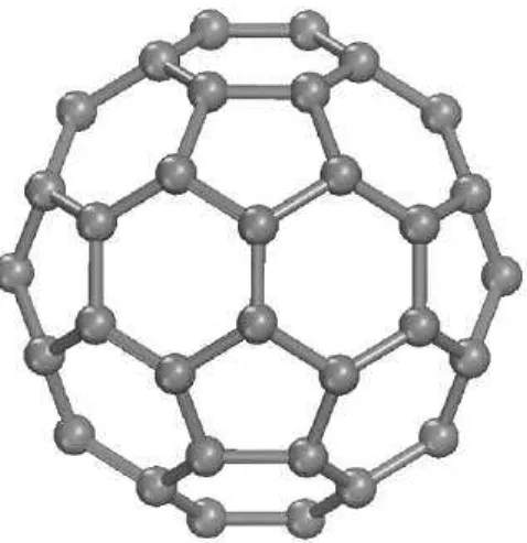
In view of the splendid technological development of the world one of the question that arises is how is it possible to maintain the current rate of advances in the electronic based industry. These advances are expected to reach a limit soon, as the silicon based technology development departs from Moore’s law. Many research groups around the world have been worked strongly to answer this question, and one promising way seems to be through the carbon based technology. The paper by Krotoet al[4] published in 1985 is remarkable because we can say that the research in carbon nano-structures had its beginning from that point.
Figure 1: Fullerene Molecule C60 with a soccer ball format proposed by Kroto et al in 1985, in his paper where they assume that carbon prefer to be in C60 form, as observed in their mass spectroscopy measurements.
Few years after Kroto’s seminal paper, another carbon allotrope was highly studied, the carbon nanotubes observed by Sumio Ijima [1], in 1991. This is another remarkable point in the nanotechnology world, since this quasi-unidimensional crystal showed promising physical properties. In a didactic model, the carbon nanotube may be understood as a single graphite layer rolled up to form a cylindrical structure, known as single walled carbon nanotube (SWCNT).
Figure 2: Schematic representation of a singlewalled Carbon nanotube, Like the structural model proposed by Ijima in 1991 ref. [1].
the main topic of this thesis, the search by new nanostructures in which the electronic properties may be applied in novel types of electronic devices or which may be useful in the newly emerging area of spintronics [7].
1.1 The Graphene Systems
The year was 2004, when a paper by Novoselovet al [8], employing the scotch tape method for exfoliation, demonstrated the existence of a single graphite layer, the so called graphene. Such monoatomic thin layer formed only by carbon atoms, is endowed with surprising physical properties, such as high electrical and thermal conductivities as observed experimentally. Since the beginning of the 2000’s, graphene has been the gold mine for many researches, in physics and chemistry especially.
Graphene is a remarkable material because it was the first 2D crystal to over-come the Mermin-Wagner theorem, which states that a 2D crystal looses its long-range order, thus melting the entire lattice, under any temperature above zero K, due to ther-mal fluctuations. However, what facts are behind graphene’s interesting properties? To answer this question we should first look at the carbon atom. Carbon can be hybridized in three different forms, sp1, sp2 and sp3. Here we will take into account just the sp2 hybridization, which is the one in which graphene is found to be. In that case the orbital 2s and two components of 2p are superposed, where we can represent them in the Dirac notation as |2pxi and |2pyi states, in such way that we obtain a planar hybridization.
Thus the three quantum-mechanical states are given as following:
|sp21i= √1
3|2si − r
|sp2 2i=
1
√
3|2si+ r
2 3
√
3
2 |2pxi+ 1 2|2pyi
|sp23i=− 1
−√3|2si+ r
2 3
√
3
2 |2pxi+ 1 2|2pyi
These orbitals are oriented in the xy-plane and they have a 120o angle
sep-aration between each other. Because of this hibridization, graphene is condensed in a honeycomb lattice, on which the two neighboring carbon atoms are not equivalent, what leads graphene to have a non-Bravais lattice. Indeed we can consider graphene as being composed of two triangular Bravais lattices intertwined, they are the sublattices A and B [9, 10]. The distance between two subsequent carbon atoms is 1.42 ˚A, this value is approximately an average of a single carbon bond C-C and a double carbon bond C=C distances.
The three vectors which connect an atom in latticeAto the other in the lattice B are given by:
~ V1 =
a
2 √
3bi+bj
~ V2 =
a
2
−√3bi+bj
~
V3 =−abj
And the real space lattice vector which span the graphene’s hexagonal lattice are expressed as,
~ a1 =
√
3 2 abi,
a
2bj
~ a2 =
√
3 2 abi,−
a
2bj
Where a=|a~1| = |a~2| = 1.42 ×
√
3 = 2.46 ˚A, this value is the lattice constant for two dimensional graphite. In Figure 3 we can see the schematic view of sp2 hybridization as well as for the honeycomb lattice.
Figure 3: a) representation for atomic orbitals in the sp2 hybridization for carbon case, which has a 120o between each other. b)Honeycomb lattice, the vectorsV1,V
2 and V3 are connecting an atom in the sublatticeAwith it’s neighbours in the sublatticeB separated by a distance of 1.42 ˚A. The vectors a1 and a2 are the base vectors which span the graphene structure.
of its hexagonal Brillouin zone. Also, a linear energy-momentum dispersion around what is called Dirac cone [11] is observed. Because of this property, low energy elec-trons in graphene may behave like relativistic particles [12, 13] thus allowing graphene to show outstanding ballistic transport properties, with a long coherence length, which makes graphene an excellent platform for studying many physical phenomena. Therefore, graphene is known to have a very high measured carrier mobility, up to 15×102 cm3/V s [14]. In addition to this, graphene still has a high Young’s modulus and strength and its thermal conductivity is comparable to those associated to carbon nanotubes [15–17].
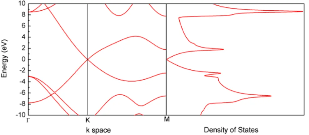
All those outstanding properties associated to graphene places this 2D-crystal among the most promising materials candidates for replacing silicon in electronic applica-tions for the future. In such asin devices like high frequency transistors, supercapacitors or touch screens [18]. However a pristine graphene sheet have no band gap as we can see in the band structure plot depicted in Figure 4.
Figure 4: Graphene band structure in the k-space and the respective Density of States, calculated using the Density Functional Theory (DFT). The Fermi energy was set up in the zero.
We can observe the link between the valence band and conduction band, ex-actly in theKpoint in the reciprocal space. Since many electronic devices interesting for technological applications are dependent of a switching character, the absence of a band gap in graphene is not desirable for some relevant applications, such as in transistors situation. Then for a real use of graphene in electronic applications, something must be done to find out a way to open a band gap in graphene based systems.
1.1.1 Graphene Nanoribbons
a graphene nanoribbon is built. Theoretical calculations have predicted that this kind of carbon structure exhibit electronic properties which make them attractive for the fabri-cation of nanoscale devices [19, 20]. It is also known in the literature, that the size of the energy gap and ribbon width are inversely proportional to each other [21, 22], and also depend on the chemical nature of the edges of the ribbon. This limits the range of widths for which the semiconducting behaviour is found. In general, graphene nanoribbons with widths smaller than ten nanometers are able to show semiconducting properties [2].
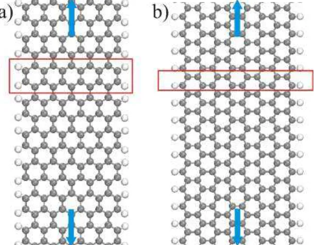
The edge termination exerts a strong influence in nanomaterials. The two most studied types of edge terminations in the graphene nanoribbon are the zigzag graphene naonoribon (ZGNR) and armchair graphene nanoribbon (AGNR) [23]. Figure 5 depicts an exemplification of these structures. In order to perform calculations based in this kind of periodic structure, periodic boundary conditions are usually applied.
Figure 5: a) Periodic AGNR the arrows indicate the continuousness, and the red box shows the unit cell for computation. b) The ZGNR depicted as in the previous case.
From the experimental point of view, there are several methods to fabricate a GNR including unzipping a carbon nanotube, lithographic methods, and recently a chemical method based in an intermolecular colligation using polymers as precursors for the bottom-up fabrication, have been proposed, as presented in Ref. [23]. The paper by Cai and co-workers opened precedents for the fabrication not only of a linear GNR, but also for, other types of configurations such as Chevron-type structure and the junction of two or more ribbons.
Figure 6: a) Reactions scheme using 6,11-dibromo-1,2,3,4-tetraphenyltriphenilene monomer passing by different temperatures to form a new GNR. b) STM images con-taining several Chevron-type GNRs, adapted from Ref. [2]
1.2 Boron Nitride
Boron Nitride BN is found in nature, in several different structural configu-rations, such as diamond like, cubic, wurtzite and also in a hexagonal phase similar to that of the graphite, called hexagonal boron nitride,h-BN. It is in the last structure that lies the focus of this work, Boron and Nitrogen forming covalent bonds. However there is a considerable difference in the Pauli electronegativity between the two atoms, thus this bond has some ionic features, existing an intrinsic electric dipole though the bonding. This leads to a charge transfer, where the electrons tend to be more localized in N atom. Moreover h-BN is known to have a huge electronic gap of the order of 5-6 eV [24]. The first applications of BN date from the 1940’s, in the cosmetic industry [25], as lubricants, due to its high stability at room temperature and due to its insulating properties, being useful as a substitute for graphite [26]. Chemical vapor depositionCVD growth of h-BN has been reported since the 70’s [27] and the primary evidence about single layer h-BN dates from 1990 [28].
h-BN composites the B atom is found at asp2 hybridization and regarding the primitive cell of both cases, they are isoelectronic, containing 12 electrons. In geometrical picture a h-BN single layer has an energy gap larger than the bulk phase for this material, once the Van der Waals interaction is missing.
In Figure 7 we can see a plot of Density of States (DOS) for an infinite h-BN sheet. The gap presented in that calculation is 5.80 eV, where it has been predicted by an ab-initio calculation. All those characteristics mentioned previously, makes h-BN a very good insulator in relation to graphene or even the ideal substrate for the latter. After the successfully growth of a pristine h-BN single layer, other geometrical configurations became possible, like the boron nitride nanoribbons BNNRs, boron nitride nanotubes BNNT, nanocages and other, which brought a enormous possibilities of technological applications to this material. As graphene, h-BN also have many physical properties very interesting, such as half metallicity which is a property very desired for spintronics purposes.
Figure 7: DOS of a BN sheet carried out using DFT method and under GGA picture. Here we can see the huge electronic gap presented by this 2D crystal. It has made BN a good ultra-violet light emitter [3]
Using passivation it is possible to change the electronic properties of these materials, as inserting new electronics states inside the gap for example. Among many possibilities to interfere in the electronic properties, the insertion of heteroatoms and topological defects like Stone-Wales open the horizons for several physics which are not known in this present times. Another point where passivation is important for flat systems, lies in the fact that without dangling bond saturation the geometric reconstruction takes place [31, 32], and such effect is not so interesting for some device applications. It reflects strongly in the band gap engineering of this kind of material, since switching devices for example, require the existence of a band gap. Therefore materials based on h-BN, like those shown in Figure 8 have been received more and more attention, in condensed matter research under a theoretical point of view or even in a experimental way, since the laboratory techniques are in constant improvement, like CVD method, which is seen as a promising tool, for growing such nanomaterials in a large scale framework.
Figure 8: Some nanostructures based on Boron Nitride which can be eventually applied in a such electronic/opto-electronic device, or even spintronics can be explored in the systems, by means of gap modulation using an external electric field.
1.3 Transition Metal Dichalcogenides (TMDCs)
Figure 9: General staking of a TMDC in the trigonal prismatic phase. The black sphere represent the metal, the yellow refers to the chalcogen atom.
the TMDCs group [33], and from the electronic point of view, they show elements with insulating character such asHf S2, passing by the semiconductors like,M oS2, to the fully metallic as in the N bS2 case [33]. We have focused this work on the semiconductor ones, in special on the molybdenum disulfide (M oS2) and tungsten diselenide (W Se2), since our research aims to model and propose new possibilities for semiconducting devices.
M oS2 has been studied both experimentally and theoretically. In its bulk formM oS2 is known to possess an indirect band gap or approximately 1.2 eV according to density functional theory calculations [34]. It is also predicted theoretically that a transition from indirect to direct gap is found from the bulk form to the monolayer [34]. Such prediction is confirmed by experiments, it has been found a strong photoluminescence associated to the monolayer case [35]. Furthermore recent experiments using the angle-resolved photoemission spectroscopy (ARPES), where further confirm the direct band gap for the single layerM oS2 [35], with a theoretical value of 1.9 eV [34]. Geometrically identical toM oS2, W Se2 also presents an indirect to direct transition in its bulk form to monolayer, howeverW Se2 is found to present a smaller band gap in its single layer form than M oS2, approximately 1.6 eV [36]. Furthermore, W Se2 exhibits a better electronic transport when compared toM oS2, since its carrier mobility is said to be higher than the later case. More than thisW Se2 is also more resistant to oxidation in humid atmospheres that M oS2 [37], which converts W Se2 in an interesting candidate for future practical applications.
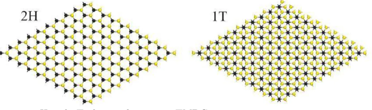
The TMDCs are very sensitive to the geometrical arrangement of the atoms, in special those specimens discussed here so far. Despite showing a semiconducting character in the hexagonal 2H (trigonal prismatic) phase, the electronic structure of M oS2 and
Figure 10: 2H and 1T phases of a generic TMDC.
2 THEORETICAL BACKGROUND
The theoretical model approach employed for calculating the electronic struc-ture of the materials studied in this work are discussed in this chapter. It is known that solving the Schr¨odinger equation is not an easy task for multi-electronic systems. Thus, along the twentieth century a few approaches were proposed in order to calculate the electronic structure of solids. Nowadays, two of those methods have been more applied in computational physics, the density functional theory (DFT) and the tight-binding (TB) method. In the following section we describe the quantum problem for many electron systems, the DFT formalism and the different approaches related to it. Then, we intro-duce our particular TB method based in a sp3d5 basis set. Finally, only the techniques for calculating electronic transport properties in nano-scaled devices within the ballistic transport regime are discussed in the final section.
2.1 The Quantum Problem
In quantum mechanics the systems are described in terms of their quantum states, such description is carried out using the Schr¨odinger equation, as :
i∂Ψ
∂t =HbΨ. (2.1)
The wave-particle duality observed for quantum particles in interference experiments, for instance, led to the postulate that the quantum state might be described by a wave function Ψ. Despite Ψ having no physical meaning by itself several information about the observable may be obtained from it using the quantum operators. In order to characterize the total energy of the system, the Hamiltonian operatorHb acts in the wave function. In the multi-electronic framework the Hamiltonian operator is written in atomic units as:
b
H =−1 2
X
i
∇2i −
1 2
X
j
∇2A
2MA − X i X A ZA riA +X i X j>i 1 rij +X A X B>A
ZAZB
RAB
. (2.2)
The first term yields the kinetic energy for the electrons Tbe. The second term is related
to the kinetic energy from the nuclei Tbn. The third factor is the attraction potential
between electron-nuclei Vbe−n, the fourth term is related to the potential resultant from
the interaction between electrons Ebe−e and the last represents the nuclei-nuclei repulsion b
Vn−n. Thus, Eq. 2.2 may be written as: b
Considering the time independence of the Hamiltonian operator, one could perform a variable separation in the wave function Ψ which exhibits a time dependence, thus:
Ψ(~r, t) = Φ(~r)Θ(t). (2.4)
Such mathematical practice yields two equations: b
HΦ = EΦ, (2.5)
i∂Θ
∂t =EΘ. (2.6)
Equation 2.5 is known as the time independent Schr¨odinger equation. Re-writing this equation in the form (Hb −Ψ)E = 0 leads to an eigenvalue problem for the Hamiltonian operator to be solved. Equation 2.6 represents the evolution of the temporal phase factor for the wave function. The solution to this equation is:
Θ(t) = Aexp(−iEt), (2.7)
with Eq. 2.7A is a normalization constant. For time independent problems in this frame-work only the spacial part of the wave function Φ(~r) needs to be considered. Observing the Hamiltonian operator (Eq. 2.2) we find that the third therm referring to the electron-nuclei coulombic interaction, turns the solubility of the problem difficult, thus it is needed to find out a valid approximation which enable us to separate the motions of the the electronic and nuclei parts since we are supposing to be working with many atoms in the system, and not just a simple problem like a single hydrogen atom. The solution to this problem, which allows decoupling the two motions is the Born-Oppenheimer approxima-tion. This theory is also known as adiabatic approximation and it is based on the fact that the difference between electron and nuclei masses is high.
2.2 The Born-Oppenheimer Approximation
The Born-Oppenheimer approximation has considerable importance in con-densed matter physics. It is the starting point to several other approximations which aims to describe the electronic structure of the matter. This approximation was proposed by M. Born and J.R. Oppenheimer in 1927 [39]. This approach is based on the fact that the rate between the electron mass and the electronic nuclei mass is very small. Such observation allows to consider that the nuclei can not move as fast as the electrons, thus considering the nuclei at rest. Therefore, the termTbn in 2.3 becomes negligible. In other
be written as:
Φ(~r) = ψ(~re)Ω(~rN). (2.8)
Substituting 2.8 in 2.5 we have, b
Hψ(~re)Ω(~rN) = Eψ(~re)Ω(~rN). (2.9)
where the positions of the electrons are labelled as~re and for the nuclei positions ~rN.
At this point we are able to solve the electronic problem. Since we are assuming that the nuclei positions does not changes in time. The interaction nuclei-nuclei can be taken as a parameter of the system, thus disregarding it as a variable. Furthermore the kinetic energy related to the nuclei is not taken into account, then we can reduce our problem to,
b
Heφ(~re) = Eeφ(~re). (2.10)
It is important to emphasize the fact that in the electronic problem the function Ω(~rN)
is a constant, since the nuclear positions are kept frozen. Here Hbe is called electronic
Hamiltonian operator. It is written as b
He =Tbe+Vbe−n+Ebe−e. (2.11)
After this simplification we can solve the electronic problem and find the wave function
ψ(~re) which corresponds to the electrons of the system, and consequently the electronic
energy Ee.
Even considering only the electronic problem it is still a difficult problem to be solved specially for system containing many electrons. Nowadays there are many methods to calculate the electronic structure of the matter, among the most applied are the Tight-Binding (TB) [40] and the Hartree-Fock (HF) based methods [41]. In these two examples the electron-electron interaction is not totally considered, what leads to a loss in the knowledge of the fine structure of the system. Thus in order to obtain more accuracy, we decided to employ in some sections of this work the Density Functional Theory (DFT) [10]. DFT has been employed in the study of molecules and solids since the nineties. Its use has been growing steadily due to the advances of computational tools and to its relatively low computational cost compared to other HF based methods.
2.3 DFT Method
as physics, chemistry, material sciences and engineering. A very interesting example of DFT application is the work by Umemoto, Wentzcovitch and Allen [42], where they have used DFT to model planetary formation. The DFT approach is based in obtaining the electronic density associated to the problem, which reduces the problem to a variable that depends only on the three spatial coordinates. Differently from the HF which depends on 3N variables, where N in the number of electrons. Such property of the DFT framework is very important from the practical point of view, since it allows for the lowering of the computational cost.
Density Functional Theory has been proposed within two seminal papers in the sixties, by Hohenberg and Kohn [43] and Kohn and Sham [44] where they describe the details of the theory and a methodology to apply it. However the basics of DFT lies in a theory proposed in the late twenties, the so called Thomas-Fermi approximation [45], which was proposed independently by Thomas in 1927 and Fermi in 1928. Thus due to the importance of Thomas-Fermi model to DFT we will make an introduction to this subject.
2.3.1 The Thomas-Fermi Theory
Historically L.H. Thomas was the first researcher to propose what we know as the Tomas-Fermi model, in 1926. His work aimed to develop a theory which was based on approximate fields for heavy atoms, in order to model quantum observables. This theory is based in four assumptions, which are:
1. Relativity corrections are negligible.
2. In the atom there is an effective field given by potential the V, depending only on the distance r from the nuclei, such that
V −→0 as r −→ ∞
Vr −→ Ze, the nuclear charge, asr −→ 0
3. The electrons are uniformly distributed in the phase space with six dimensions. Each electron pair occupies a volume of h3, whereh is the Planck’s constant.
4. The potential V is itself determined by the nuclear charge and the corresponding electronic distribution.
If we take an electron gas as a physical system enclosed onto a cubic box with a volume v, we could apply the periodic boundary conditions such that,
exp(ikxv
1
3) = exp(ik
yv
1
3) =exp(ik
zv
1
Thus starting from the plane wave solution to the free particle,
φk(r) =
1
v12
exp(iK ·r). (2.13)
Where the energy is given by,
ǫk=
¯
h2k2
2m . (2.14)
Then we can find, thatkx=nx2π/v
1 3, k
y =ny2π/v
1 3, k
z =nz2π/v
1
3, wheren
x, ny and nz
are integers. The possible wave vectors are those which in the k space are given by multiples of 2π/v13, and each k point occupies a volume Ω
k given by,
Ωk =
8π3
v . (2.15)
The total volume in reciprocal space will be given by a sphere of radiuskF:
Ωt=
4 3πk
3
F. (2.16)
Considering the number of electrons ( N ), and that each state k has two spin components, spin α and spin β we have,
N = 2Ωt Ωk
= k 3
Fv
3π2. (2.17)
Now we can write down an expression for the electronic density:
ρ= N
v = k3
F
3π2. (2.18)
If we write down the classical equation to the electron in a k state, under a electrostatic potential u(r), we will realize that within the volume of an atom the vector k must be related to the energy by,
ǫF =
¯
h2k2
F
2m −eu(r). (2.19)
Since there are no singularities in the charge density for R ≤ r, the potential u(r) and electric field shall be continuous, so
u(r) = Zefe
r , f or r > R. (2.20)
Where R is the radius for a positive ion with the chargeZef to be determined.
Thus the relations for r=R must be,
u(R) = Zefe
R and
du(r)
dr r =R
=−Zefe
R2 . (2.21)
Once an inner electron must be bound, its energy is less than the potential energy−eu(r) at the surface of the shell. In this situation we have,
¯
h2k2
F
2m =e[u(r)−u(R)]. (2.22)
At this point we can derive an expression to the electronic density, using the Poisson relation,
∇2u(r) =−4πeρ(r), (2.23)
ρ(r) = 1 3π2
2me ¯ h2 3 2
It is important to note here, that the equation 2.24 should be used when u(r) ≥ u(R) otherwise the density will be equal to zero. In order to simplify the calculations we could translate 2.24 to spherical coordinates, thus resulting in:
˜
u(r)≡ r
Ze[u(r)−u(R)], (2.25)
performing a simple change of variables, wherex= r a and,
a =
9π2 128Z
1 3 ¯h2
me2 = 0.88534Z
−13 h¯ 2
me2. (2.26)
We obtain the Thomas-Fermi relationif we take the second derivative, such that
d2u˜
dx2 = ˜
u32
√
x. (2.27)
Applying the boundary condition, we have ˜
u(0) = 1. (2.28)
Forx=R/a, we will have ˜u(x) = 0, and from 2.25 we know,
du˜(r)
dr R
= u(r)−u(R)
Ze R + ru
′(r) Ze R . (2.29)
The first term in the right side of the equation 2.29 is zero whenr =R and knowing that
u′(R) =
−Zefe/R2,
xu′(x) = −Zef
Z . (2.30)
At this point, under this conditions we can obtain the number of electrons inside the sphere. Combining 2.24 and 2.25 we find,
4π
Z R
0
ρ(r)r2dr=Z
Z x
0
x√xu˜(x)32dx, (2.31)
and paying attention to the fact that√xu˜′′ = ˜u32, we have:
Z
Z x
0
xu˜′′dx=Zu˜(0) + ˜u(x). (2.32) Now combining equations 2.28 and 2.30 It results in,
4π
Z r
0
ρ(r)r2dr =Z −Zef. (2.33)
The expression to the charge density (Eq. 2.24) can be derived by the variational principle, in which the total energy is a functional of the electronic density ρ, written in the form:
E[ρ] =ξ
Z
ρ53d3r−e Z
ρuNd3r−
1 2e
Z
ρued3r+UN N. (2.34)
Here
ξ = 3h 2 10m 3 8π 2 3 , (2.35)
and uN is the potential related to the nuclei, ue is the potential due to the electrons.
The first integral in 2.34 corresponds to the kinetic energy term for the electrons, the second integral is the energy due to the electron-nuclei interaction, the third integral is the term which describes the electron-electron interaction, and UN N is the interaction
Now we can write the Thomas-Fermi relation. Whether the energyE[ρ] has a stationary value in relation to the densityρand the number of electrons is kept constant in relation to the time. We obtain the following relation:
δ δρ
E[ρ]−u(R) Z
ρd3r
= 0. (2.36)
To finalize this exposure about this pioneer theory, we write the Thomas-Fermi-Dirac functionalE[ρ], which include the exchange term proposed by Dirac in 1930,
E[ρ] =ξ
Z
ρ53d3r−e Z
ρuNd3r−
1 2e
Z
ρued3r+UN N −
3 4e 2 3 π 1 3 Z
ρ43d3r. (2.37)
If E[ρ] is stationary in relation to variations of the electronic density ρ we have the equation of Thomas-Fermi-Dirac to the electronic density.
ρ= 8π
3h2(2me) 3 2
(2me3)1 2
h +
u−u(R) + 2me 3
h
1 23
. (2.38)
2.3.2 The Fundamental Theorems
Density Functional Theory is based on two elementary theorems, proposed by Honhenberg and Kohn in 1964 [43] as an improvement of the Thomas-Fermi method. The first theorem states,
”The ground state energy from Schr¨odinger’s equation is a unique functional of the electron density.”
Considering a number of electronsN, inside a large box and moving under the influence of an external potential u(r), and taking into account the coulombic repulsion, we can prove this theorem by reductio ad absurdum. Since the Hamiltonian for this system has the form:
b
H =Tb+Vb +U .b (2.39)
where, b
T ≡ 1
2 Z
∇ψ∗(~r)
∇ψ(~r)d~r, (2.40)
b
V ≡
Z
u(~r)ψ∗(~r)ψ(~r)d~r, (2.41)
b
U = 1 2
Z 1
|~r−~r′|ψ
∗(~r)ψ∗(~r′)ψ(~r)ψ(~r′)d~rd~r′. (2.42)
Assuming for simplicity that the ground stateψis not degenerate we can define the electronic density as:
ρ(~r) =X
i
ψ∗(~r)ψ(~r) =hψ|X
i
δ(~r−~ri)|ψi. (2.43)
Now if we consider another external potentialu′(~r), leading to a new HamiltonianHb and
electronic densityρ(~r), then:
E =hψ|Tb+Vb +Ub|ψi<hψ′|Tb+Vb +Ub|ψ′i, E′ =
hψ′
|Tb+Vb′+Ub |ψ′
i<hψ|Tb+Vb′+Ub |ψi.
Consequently,
hψ|Hb|ψi<hψ|Hb′
|ψi=hψ′ |Hb′
|ψ′
i+hψ′
|Vb −Vb′ |ψ′
i. (2.44)
Writing Eq. 2.44 in terms of the energy we will see that,
E < E′+
Z
[u(~r)−u′(~r)]ρ(~r)d(~r). (2.45)
Thus for the termhψ′|Hb′|ψ′i,
E′ < E+ Z
[u′(~r)−u(~r)]ρ(~r)d(~r). (2.46) In other words,
E+E′ < E′+E. (2.47)
Thus, if we had assumed the same electronic densityρ(~r), with u6=u′, we are
facing an absurd, since ψ 6=ψ′. This shows that the first theorem is valid.
The second theorem states that
”The electronic density that minimizes the energy of the overall functional is the true electronic density corresponding to the complete solution of the Schr¨odinger equation.” This statement is proven in the following steps,
E[ρ] =hψ|Tb+Ub+Vb|ψi. (2.48)
In that case we set ρ(~r) as an electronic density for a given state ψ, which is not necessarily the true density that comes fromHb =Tb+Ub+Vb that will be called ρ0, thus:
ρ6=ρ0 =⇒ψ 6=ψ0, then, E > E0
ρ=ρ0 =⇒ψ =ψ0, then, E =E0
If we re-write the equation 2.48 we can have it in the form,
E[ρ] =hψ|Tb+Ub|ψi+hψ|Vb|ψi, (2.49) or just,
E[ρ] =F[ρ] +hψ|Vb|ψi. (2.50)
Here F[ρ] is an universal functional that is valid for every Coulomb system and the termhψ|Vb|ψi depending on the system. In an analogue way we can write the same thing to the exact electronic density, therefore
E[ρ0] =F[ρ0] +hψ0|Vb|ψ0i. (2.51) Then, ifψ0 represents the true ground state, and ψ another state, consequently ρ0 and ρ are defined by any external potential. From the variational theorem we have:
hψ0|Tb+Ub|ψ0i+hψ0|Vb|ψ0i<hψ|Tb+Ub|ψi+hψ|Vb|ψi, (2.53)
F[ρ0] +hψ0|Vb|ψ0i< F[ρ] +hψ|Vb|ψi. (2.54) Thus,
E[ρ0]< E[ρ]. (2.55)
So now we have proven the second Hohenberg-Kohn theorem.
2.3.3 The Kohn-Sham Equations.
So far we have discussed a theory which can leads to a solution for the electronic structure problem. However one year after the Hohenberg-Kohn work, another paper by Kohn-Sham was published [44]. To solve the ground state problem self-consistently including the exchange interaction. Thus according to the Ref. [43] the ground state energy for an electron gas, where the particles are interacting with each other is given by:
E = Z
u(~r)ρ(~r)d~r+1 2
Z Z ρ(~r′)ρ(~r)
~r−~r′ d~rd~r
′+G[ρ]. (2.56)
In equation 2.56 u(~r) is the static potential which is external to the electron gas, ρ(~r) is the electronic density and the term G[ρ] is an universal functional of density, defined as:
G[ρ]≡Ts[ρ] +Exc[ρ]. (2.57)
In the Kohn-Sham formalism, the Ts[ρ] term stands for the kinetic energy related to a
non-interacting system, and the term Exc[ρ] is the exchange and correlation interaction
of an interacting system. Then, if the density can vary slowly it is possible to write down the following equation to the exchange-correlation term:
Exc[ρ] = Z
ρ(~r)ǫxc(ρ(~r))d~r. (2.58)
In this case ǫxc(ρ(~r)) is the exchange and correlation energy per electron in an uniform
electron gas where the density isρ(~r). By the variational theorem, the minimization for Eq. 2.56 requires the following condition:Z
δρ(~r)d~r= 0. (2.59)
Leading to,Z
δρ(~r)
ϕ(~r) + δTs[ρ]
δρ(~r) +µ(ρ(~r))
d~r= 0. (2.60)
In Eq. 2.60,
ϕ(~r) = u(~r) +
Z ρ(~r′)
~r−~r′d~r
and
µ(ρ(~r)) = d(ρǫxc(ρ(~r)))
dρ . (2.62)
Solving Eq. 2.60 it is possible to find an expression similar to the Schr¨odinger equation, involving eigenvalues. Such equation has the form:
−12∇2+uKS
ψi(~r) = εiψi(~r). (2.63)
Once,
uKS =ϕ(~r) +µ(ρ(~r)). (2.64)
uKS and µ(ρ(~r)) are respectively the Kohn-Sham effective potential and the chemical
potential of the system. The density can be obtained as,
ρ(~r) =X|ψi(~r)|2. (2.65)
The equation 2.63 must be solved self-consistently. In Figure 11 we have a schematic graphic where the self-consistent cycle is described. Finally, the Kohn-Sham energy is
Figure 11: Self-Consistent cycle to solve the Kohn-Sham equations. It begins from a trial electronic density ρ(~r) for the system. Thus the orbitals ψi(~r) are obtained. After that
it is possible to get a second value to the electronic density. The cycle is kept until a threshold value is reached for convergence.
given by,
EKS = X
εi−
1 2
Z Z
ρ0(~r′)ρ
0(~r)
~r−~r′ d~rd~r ′
+ Z
ρ(~r)[ǫxc(ρ(~r))−µ(ρ(~r))]ǫxc(ρ(~r)), (2.66)
once, X
εi =Ts[ρ(~r)] + Z
uKSρ(~r)d~r. (2.67)
2.3.4 Exchange-Correlation Term
One of the open issues regarding the DFT technique is related to the exchange-correlation term (xc) which has no analytic form which can be applied for every systems. If we observe carefully equation 2.66 we will note that ǫxc(ρ(~r)) is not known and
approximations which have been used for obtaining acceptable results for several sys-tems. The first of those approaches is the Local Density Approximation (LDA), where the exchange-correlation energy for a system with a local density ρ is proposed to be the same as in an electron gas with the same density [46]. It’s important to emphasize that for this approximation to be valid the density must vary smoothly around a given space position. Then we can write down the following equation:
ELDA xc [ρ] =
Z
ρ(~r)ǫLDA
xc (ρ(~r))d~r. (2.68)
The functionǫLDA
xc (ρ(~r)), can be divided in two parts, one refers to the exchange and the
other to the correlation, so:
ǫLDAxc (ρ(~r)) = ǫx(ρ(~r)) +ǫc(ρ(~r)). (2.69)
Then, the corresponding exchange-correlation potential for the LDA approach is given by,
uLDA xc [ρ] =
dELDA xc
dρ(~r) =ǫxc(ρ(~r)) +ρ(~r)
dǫLDA xc (ρ(~r))
dρ(~r) . (2.70)
Now, getting back to the equation 2.69, the exchange term ǫx(ρ(~r)) can be
extracted from Hartree-Fock theory. If we take into account the Slater contribution it can be obtained for a homogeneous electron gas that,
ǫx(ρ(~r)) = −
3N e2kF
4π . (2.71)
Once we know thatkF = (3π2ρ)
1
3, the energy per volume is,
ǫx(ρ(~r)) =
Ex
V =
−3e2(2π)1 3ρ
4 3
4π . (2.72)
Writing the density ρ as a function of the Winger radius rs We get,
ρ(~r) = 3 4πrs
. (2.73)
Finally we have,
ǫx(ρ(~r)) = −
0.4582
rs
. (2.74)
The correlation term ǫc(ρ(~r)) has a high degree of complexity and has no
an-alytical solution even for an ideal electron gas. Despite of this, in 1981 Ceperley and Alder [47] published results from a quantum Monte Carlo calculation, which yields ac-curate values for the correlation interaction in many different systems. After this first proposal, Perdew and Zunger [48] took the work in Ref. [47] as parameter to deal with high (rs <1) and low (rs>1) densities.
Then the expression that describes low densities for each electron according Ref. [48] is given by:
ǫi c =
γi
1 +βi
1√rs+β2irs
. (2.75)
On the other hand, the expression to high densities is written as,
In the equations 2.75 and 2.76 the parameters for the homogeneous electron gas are given by, γ = −0.1423, β1 = 1.0529, β2 = 0.3334, C = 0.0020, D = −0.0116, A = 0.0311,
B = −0,048 in the situation where there is no polarization. There are some particu-larities about the LDA which might be mentioned, for example it’s known that LDA overestimates the atomic distances and the dissociation energies. Also, the bulk modulus is overestimated by 8 to 18 % and the band gap in semiconductors is underestimated by about 50 %.
However, when we are working with real atomic systems, the electronic density is not in general constant. Thus, in order to improve the LDA a new approach was pro-posed known as the Generalized Gradient Approximation (GGA). In this picture the gradient of density is taken into account to obtain the exchange functional Exc[ρ].
There are different proposals for how the gradient term is included in the GGA term, some of the most applied formalism in several software packages are based on the works of Perdew-Burke-Erzenhof [49] and Lee-Yang-Parr [50]. In a general way the exchange-correlation functional in the GGA is written as:
EGGA xc [ρ] =
Z
f(ρ(~r),∇ρ(~r))d~r. (2.77)
Since the main source of uncertainty in DFT is associated to the Exchange-Correlation Functional, the GGA approach brought more accuracy to the calculations, and nowadays it is a widely employed tool in atomic-molecular modelling.
2.3.5 The Pseudopotential Approach
In principle, when we are working with atomic species in the DFT framework all electrons should be considered. However for the chemical bonding process only the outermost electrons are important. In a practical way a DFT calculation is performed considering every electron in the system. For this reason, it is sometimes useful to perform the calculation considering only the valence electrons. This means replacing the inner electrons by a pseudopotential (PP), which must be as accurate as the contribution from the real electrons. This process is called a frozen core calculation. Nowadays the frozen core framework is widely more employed than all-electrons calculations. A immediate reason for this is that the computational effort is far more economic than in an AE calculation. And the results are as accurate as in an all-electrons calculation.
Hamann and Schl¨uter [51] and Troullier-Martins [52]. These particular constructions are said to be Norm-Conserving pseudopotential [53], but there are pseudopotentials where the norm is not conserved, like the one proposed by Vanderbilt [54]. An ab-initio pseu-dopotential in its construction always starts from an all electron calculation, and the PP must keep some important properties in order to conserve the norm:
1. The eigenvalues εi from an All-Electron (AE) calculation must be identical to the
eigenvalues εP P
i from pseudopotential.
2. The eigenvectors from AE calculation and those from PP must be the same for
r > rc where rc here is the core radius.
3. The integrals from 0 upto r, r > rc, related with charge density of AE calculation
must be equal to the obtained with the PP.
4. The logarithmic derivative of pseudo-eigenstate must converge to the AE eigenstate when r > rc.
Properties 3 and 4 are closely related with the pseudopotential transferability [55], which is the capability of a pseudopotential to be used in different kinds of chemical environments, since atoms in crystals, molecules or even in a gas phase may not behave equally. Figure 12 shows the schematic behavior as expected for a PP. Showing the expected relation for the pseudo eigenstate and the AE eigenstate as well as the potentials from pseudopotential and AE calculation.
Since we are interested in ab-initio pseudopotentials, then we should begin from the Kohn-Sham equation,
[T +uKS(~r)]ψi(~r) =εiψi(~r). (2.78)
Adopting spherical coordinates to solve Eq. 2.78, we can write down the following ex-pression:
−12 d
2
d~r2 +
l(l+ 1) 2~r2 +u
KS[ρ, ~r]
~rRnl(~r) =εnl~rRnl(~r). (2.79)
WhereuKS[ρ, ~r] is the self-consistent potential for one electron. For sake of simplicity we
will refer to this term asu[ρ, ~r], and it is given as:
u[ρ, ~r] = −Z
~r +uH[ρ, ~r] +uxc[ρ(~r)], (2.80)
where ρ(~r) is the sum of whole electronic density and uH[ρ, ~r] is the Hartree potential
which is related to every Rnl(~r) state. The last term uxc[ρ(~r) is the potential due to the
Figure 12: Schematic representation for the pseudopotential (full line in blue) and AE potential (dot line in green), and the corresponding eigenstates. The vertical dot line in black represents the core radius, satisfying the conditions 1 and 2.
After doing this this calculations, we obtained the eigenvectors of the all-electron calculationRAE
l (~r) and its respective eigenvaluesεAEl . Thus it is possible to start
a parametrization of the pseudopotential, following the properties listed above. Therefore the property 1 is written mathematically as,
RP P
l (~r) =R AE
l (~r) when r > rc. (2.81)
For property 2 we have,Z
rc 0 |
RP Pl (~r)|2~r2d~r = Z rc
0 |
RAEl (~r)|2~r2d~r (2.82)
and finally,
εP Pl =ε AE
l (2.83)
After we have obtained the AE potential and eigenfunctions we can set up an analytic cutoff function f(~r), going to 0 when~r →0, and tending to 1 as fast as ~r3. A
rc must be chosen for each l, in general 0.5 to 1.0 times the radius rml of the outermost
peak of ul. Then we can construct the following potential:
uP P
1l =u
1−f
~r rc
+clf
~r rc
, where= (
f(~r
rc)→1 if ~r→0.
f(~r
rc)→0 if ~r→ ∞.
(2.84)
adjustment constant in order to ensure the absence of singularities. Thus a pseudo-eigenvector wP P
1l can be proposed and fitted to coincide with
the radial solution of Kohn-Sham equation, following the property 1 if we make use of a fitting constantγl as following,
γlwP P1l (~r)→R AE
l f or ~r≥rc. (2.85)
Then to have the other properties satisfied 2-4, we need normalize wP P
1l , so we will have
a definitive pseudo-eigenvector labelled as RP P l
RP Pl =γl
wP P1l +δl~rl+1f
~r rc
. (2.86)
Where δl is the smallest solution for the normalization equation,
γl2 Z ∞
0
wP P1l +δl~rl+1f
~r rc
2
d~r= 1. (2.87)
Now that we have the knowledge about the pseudo-eigenfunction we can obtain a potential related to this one, by an inversion of a Schr¨odinger type equation. It is important to emphasizes the fact that the potential like this is not a ionic potential, this is the screened potential (scr).
uP P
scr,l =εl−
l(l+ 1) 2~r2 +
1 2~rRP P
l (~r)
d2
d~r2[~rR
P P
l (~r)]. (2.88)
So far we have an atomic pseudopotential. To make it useful for another self-consistent process it is needed to find out an ionic PP from equation 2.88. It is important to the improvement of transferability of the PP, allowing its employment in several chemical environments. The ionic PP is obtained removing the Hartree potential
uP P
H (~r) and the exchange-correlation term uP Pxc (~r) from the screened potential,
uP Pion,l(~r) = u P P
scr,l(~r)−u P P
H (~r)−u P P
xc (~r). (2.89)
Here is not hard to realize, that each component of the angular momentum of the wave function, feels a different potential. In that case we should set-up an ionic pseudopotential operator like,
b
uP P
ion(~r) = u P P
ion,local(~r) + X
l
uP P
nonlocal,l(~r)Pbl. (2.90)
Where uP P
ion,local(~r) is a local potential. The non-local potential comes as a projection of
l-th angular momentum of the wave function, then it is defined as,
uP Pnonlocal,l(~r) =u P P
ion,l(~r)−u P P
ion,local(~r). (2.91)
Indeed the potential presented in Eq. 2.91 is a semi-local potential.
[56] formulation foruP P
nonlocal,l(~r) term, which states that non-local term has the form:
uKBnonlocal,l(~r) =
|uP P
nonlocal,l(~r)Φ P P,0
l (~r)ihΦ P P,0
l (~r)u P P
nonlocal,l(~r)|
hΦP P,l 0(~r)|uP P
nonlocal,l(~r)|Φ P P,0
l (~r)i
. (2.92)
Where ΦP P,l 0(~r) is the pseudo-function used as atomic reference, including the angular momentum component. In summary a very good strategy to construct the PP is to make it as close as possible to the conditions on what it will be employed. Further reading can be found in the references [51, 56].
2.3.6 Base Functions
After defining the pseudopotentials, and the orbitals via DFT, the space re-lated to the orbitals radius has no limitations extending to infinite. Indeed It turns the calculation hard to be carried out. It is very convenient to define a cutoff radius for each orbital, thus imposing a confinement. The calculation become much more easy to be carried out. Such feature may be obtained using a basis set, based on multiple ζ the-ory [57, 58]. Then the interaction between atomic orbitals is reduced for those, in which there is an overlap between its wave functions. Numerically this procedure is observed as a reduction of the terms in the Hamiltonian matrix which are different from zero, as well as in overlap matrix. The diminution in the terms to be calculated in the matrix, brings the possibility of working with systems containing a considerable number atoms, the so called Order-N calculation [59]. The atomic orbital is given by the product of a radial function and a spherical harmonic function:
φlmn=RlnYlm. (2.93)
The radial function is centred in the atomic nucleus. Increasing the number of functions to describe the radial part, the complexity and accuracy of the orbitals increases as well. The first function in that family is the single-ζ (SZ), It is the most simple function in this context, and they are obtained from the Schr¨odinger equation solution for a single atom, based in the pseudopotential corresponding to the specific chemical specie,
− 1
2r d2
dr2r+
l(l+ 1)
2r2 +Ul(r)
φl(r)−(ǫl+δǫl)φl(r). (2.94)
When we cutoff the range of the atomic orbital, we are limiting the action of that state, which in principle should be infinite. Then we are neglecting a small amount of energy. Thus to equilibrate this problem a small value in the energy δǫl is added to the orbital
energy in Eq. 2.94. This energy shift keeps the wave function normalization and it is a good way to impose the confinement.
split valenceframework [60]. Here the orbitals are given by a fixed linear combination of Gaussians. In that sense the secondζ orbital φ2ζ is a continuity of φ1ζ for a given range,
as following:
φ2lζ(r) = (
rl(a
l−blr2) if r < rsl
φ1lζ(r) if r≥rs l
(2.95)
Where al and bl are continuity constants, determined at rsl, then it is defined the first
and second order ζ functions. This second order function is that was widely employed in this theses through the Spanish Initiative for Electronic Simulations with Thousands of Atoms SIESTA method to carry out the results presented here, further information about the package can be found in Ref. [61].
2.4 Slater-Koster Tight Binding
To solve the secular equation associated to atomic systems is not an easy task even nowadays. As proposed originally by Block [62] the linear combination of atomic orbitals (LCAO) method, may imply in a significative challenger for the modern super computers. Facing the same difficulties in the fifties, Slater and Koster (SK) proposed a simplified version of LCAO, in their seminal work [63]. In a rigorous application of LCAO, one must define an atomic functionχµ(~r−R~), for every atom in the unit cell located at
position R~. Thus the linear combination φµ of those atomic orbitals may be written as
follows:
φµ(K, ~r~ ) =
1
√ N
X
R
ei~k·R~
χµ(~r−R~). (2.96)
Therefore the Hamiltonian matrix elements are given by:
Hµν(~k) = Z
φ∗µ(K, ~r~ )Hφb ν(K, ~r~ )d3r. (2.97)
Hereχµ(~r−R~) is constructed in the same form as in Eq. 2.93, which means that for every
Hamiltonian element, an integral like in Eq. 2.97 must be solved. If we consider systems where the d orbitals play important role, the Hamiltonian matrix rank might become very large, resulting in a challenging computational work.
On the other hand, when the SK method is applied, the integral is substi-tuted by a fitted potential (parameter), furthermore one may choose the most interesting energy range for any problem, for instance the energy involving the valence or conduc-tion bands in a crystal, then discarding many integrals. Considering the orbitals s, p and d, between atoms of the same chemical type, ten hopping (overlap) are considered
Vssσ, Vspσ, Vppσ, Vsdσ, Vpdσ, Vddσ, Vppπ, Vpdπ, Vddπ, Vddδ, the same set of potentials should be
Figure 13: Different bonding types,σ, π, δ, represented in hopping energiesVspσ,Vpdπ and
Vddδ.
aware that when dealing with interaction between different chemical species, the number of parameters is fourteen due the anti-symmetric directed orbitals,psσ, dsσ, dpσ, dpπ. In figure 13 the different bonding types are sketched, using theVspσ, Vpdπ and Vddδ hopping
energies.
In the appendix A, the entire set of SK equations is written for the sp3d5 orbitals. It is also important to mention that the parity of the integral is given according the following rule:
hL|Hb|L′
i= (−1)L+L′
hL|Hb|L′
i. (2.98)
Where L represents the angular momentum of each orbital. In the equations discussed in the appendix A, l, m, n, stands for the direction cosines, of the involved bond.
2.5 Ballistic transport
Figure 14: Two 2DEG separated by a narrow channel, the left 2DEG has a small difference in the chemical potentialδµ in relation to the right one.
Let’s imagine two reservoirs containing a two dimensional electrons gas (2DEG) each, spatially separated by empty space. Assuming that the first reservoir has a small difference in the electron density (δn) in relation to the second one, then we link both 2DEG by a narrow channel. Thus a diffusion current J~should flow through the channel, carried by the electrons in the energy range between Ef (Fermi level) and Ef +δµ. In
this context we can define the small difference in the electron density (δµ) as being the chemical potential difference between the reservoirs. One could describe the conductance in such system, by generalizing the Einstein relation [40], as following:
σ =e2ρ(Ef)D. (2.99)