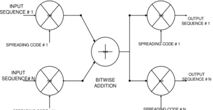
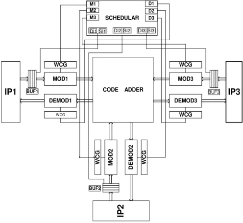
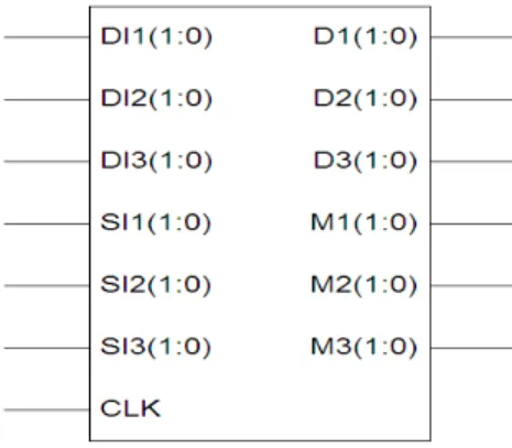
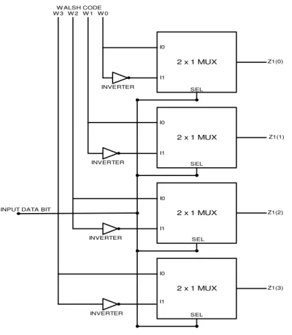
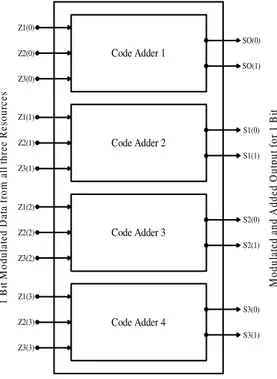
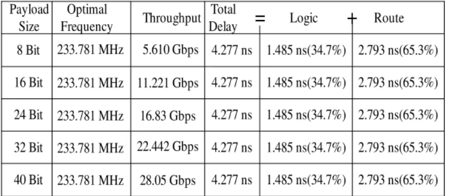
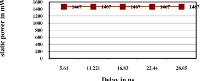
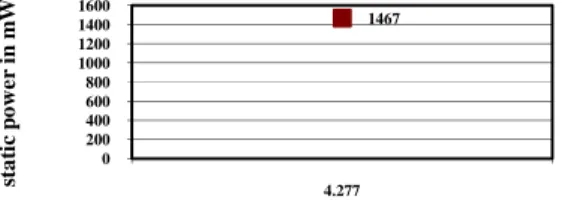
Performance Evaluation of CDMA Router for Network-On-Chip
Texto
Imagem

Documentos relacionados
instituiu o SIREP – Sistema Integrado de Registro de Preços, que se destinava a servir como orientação para a Administração como ferramenta de apoio aos gestores públicos
Os ensaios para determinação da temperatura durante o processo de furação por escoa. mento foram realizados sob as melhores condições de trabalho que o processo
Dispõe sobre a participação, hospedagem, entrada em locais onde se realizarão os eventos relacionados aos Jogos Rio 2016 e circulação em viagens pelo Brasil das crianças
O Outlook pode ajudá-lo a se proteger do lixo eletrôni co Para evitar spam, recomenda-se deixar
Após selecionar a DAV que deseja faturar, pressione a tecla “Enter” do teclado e confirme a operação e aguarde até ser mostrado a tela para informar o valor da forma de
Destruir ou danificar florestas ou demais formas de vegetação natural, em qualquer estágio sucessional, ou utilizá-las com infringência das normas de proteção em área considerada
CONDUZIR a bola progredindo para a baliza, com pequenos toques da parte interna e externa dos pés, mantendo a bola controlada, e REMATAR acertando na baliza.. Em posse da bola,
Como decorrência da revisão da literatura e da discussão empreendida, concluiu-se que: o tabagismo tem efeito deletério sobre a saúde bucal, constituindo-se no maior fator de risco
