Dayane Alfenas Reis
Robustness Analysis and
Enhancement Strategies for
Quantum-dot Cellular Automata Structures
Brazil
To Thiago Fernandes Leão and Nicolas Reis Cotrim,
Acknowledgements
I would like to express my absolute gratitude to my advisor, Professor Dr. Frank Sill Torres for his patience, motivation, and immense knowledge. His guidance was fundamental along these two years in which we have been working together. Always candid and helpful, his effective commentaries and corrections in my writings yield me a tremendous growth as a researcher.
I also would like to thank Professor Dr. Omar Paranaiba Vilela Neto for sharing his strong background in QCA through the Nanocomputing course, and also for giving me valuable advices regarding my research work.
To all the members of OptM Alab/ART, thank you for all the learning and the experience exchange. Of course, I am also very pleased for the enjoyable fun moments we lived together.
To my family members —of course including the "in law" ones —thank you for listening carefully, trying to assimilate and finally pretending to understand, while I tried to give reasonable explanations about my research topic.
Resumo
A nanotecnologia QCA (Quantum-dot Cellular Automata) tem sido apontada como possível sucessora para o CMOS (Complementary Metal-Oxide Semiconductor). A transmissão e o processamento de informação em circuitos QCA ocorrem sem o fluxo de elétrons, resultando em um baixo consumo de energia. Além disso, altas frequências de relógio são esperadas para os circuitos QCA futuros, além de uma menor área em relação ao seus análogos em CMOS. Não obstante as várias vantagens em comparação ao CMOS, a nanotecnologia QCA precisa superar vários desafios, a maioria deles relacionados à fabricação e à robustez. Por isso, a criação de estruturas QCA robustas e metodologias para análise de erros para QCA são passos obrigatórios para sua consolidação.
Este trabalho introduz um Simulador de Defeitos para QCA que emprega uma nova metodologia para análise de erros em estruturas. Tais erros podem ser causados por defeitos nas células ou desvios de fase inesperados nos sinais de relógio. O simulador oferece uma medida quantitativa do nível de robustez de uma estrutura, denominada taxa de simulações sem erro. Além disso, ele produz um mapa de calor através do qual é possível identificar os pontos de polarização mais fracos de uma estrutura sob determinadas circunstâncias de teste.
Depois da identificação dos pontos fracos das estruturas por meio dos mapas de calor, mudanças estruturais estratégicas são realizadas a fim de criar estruturas modificadas de robustez aumentada. Então, o desempenho dessas estruturas modificadas é comparado ao desempenho das estruturas regulares através de uma nova rodada de simulações. Testes realizados demonstraram a robustez superior dos componentes fundamentais modificados, na presença de defeitos de classes combinadas. Além disso, um leve aumento da robustez foi observado quando esses componentes foram usados para substituir componentes regulares dentro de circuitos e sistemas QCA mais complexos.
Em relação aos sinais de relógio QCA submetidos a desvios de fase, a estratégia de relógio assíncrono é proposta como alternativa ao tradicional esquema de relógio síncrono para diminuir a ocorrência de erros. O Simulador de Defeitos QCA foi usado para gerar desvios aleatórios, possibilitando a comparação entre os esquemas de clock síncrono e assíncrono. Os resultados para os testes realizados com os componentes fundamentais mostraram um aumento na taxa de simulações sem erro para desvios na faixa de 0 a π/4 radianos.
Abstract
QCA (Quantum-dot Cellular Automata) has been pointed out as a candidate for CMOS (Complementary Metal-Oxide Semiconductor) succession. The transmission and processing of information in QCA circuits occurs without flow of electrons, resulting in tremendously low power consumption. Furthermore, the design of QCA circuits generally requires less area than its CMOS counterpart and high clock frequencies are supposed to be achieved. Despite its many advantages in comparison to CMOS, QCA has to overcome several challenges, most of them related to its physical implementation and robustness. Thus, the creation of robust QCA structures as well as methodologies for error analysis for QCA are mandatory steps to the consolidation of this emerging nanotechnology.
This work introduces a QCA Defects Simulator that employs a novel methodology for errors analysis in QCA structures. Such errors may occur at output signals due to either structural defects into the cells or unexpected shifts in the clock signals. The tool provides a quantitative measure of the robustness level of the structure, named error-free simulations rate. Moreover, it produces a heat map by which it is possible to identify the weakest polarization points when the structure is submitted to structural defects testing under certain classes of defects.
After the weak polarization points in structures are identified by means of the heat maps, they undergo an addition of cells and strategical structural changes in order to create modified robustness enhanced structures. Then, the performance of the modified structures are compared to their regular counterparts. Results of the tests performed demonstrated the superior robustness of the modified fundamental components under combined classes of defects. Moreover, a slightly robustness enhancement was achieved when the modified fundamental components were used to replace their regular counterparts within more complex QCA circuits and systems.
Regarding to the robustness enhancement of phase-shifted QCA clock signals, an asyn-chronous clock strategy is proposed as an alternative to the traditional synasyn-chronous clock. The clock shifts testing at QCA Defects simulator was used to generate random shifts in the clock signals, allowing the comparison of the error-free rates for both synchronous and asynchronous clock signals strategies. The results for tests performed with fundamental components showed an increasing in the error-free simulations rate for shifts within the range of 0 to π/4 radians.
List of Figures
Figure 1 – Quantum dot examples . . . 5 Figure 2 – A QCA cell and its two possible logic states . . . 6 Figure 3 – Two different arrangements for the cells i and j. A fulfilled dot represent
a trapped eletron. The polarization of the cell i is arbitrarily established as +1. . . 7 Figure 4 – The four components and one circuit reported in (TOUGAW; LENT,
1994). . . 11 Figure 5 – Interconnects from the external clock circuit, i.e. clocking wires,
under-neath the QCA layer (CAMPOS, 2015). . . 12 Figure 6 – The cell inter-dot potential barrier behavior at the four distinct clock
phases. . . 13 Figure 7 – A QCA wire divided into four zones and their respective clock signals
(depicted in the same colors). The phase shifts are indicated next to the graphs. . . 14 Figure 8 – The four defect classes (dislocation, dopant, interstitial and vacancy)
used in this work. They are exemplified through a wire in which the fourth (middle) cell is always defective. . . 21 Figure 9 – The boundaries for the standard deviation in the clock signal phase. . . 22 Figure 10 – Methodology flow chart. . . 33 Figure 11 – The boundaries for displacement/misalignment of a cell in the QCA
Defects Simulator. The cell is allowed to occupy any position within the limits of the square ruler. Four extreme placements for a defective cell are shown through the QCA wire example. . . 37 Figure 12 – The two error analysis module interfaces may be accessed through the
shortcuts highlighted in red, which were integrated in the QCADesigner main menu. . . 39 Figure 13 – The two distinct perspectives for the ‘Error Exploration Settings’ window. 39 Figure 14 – The error analysis module interface for output files setting and
charac-terization round starting. The basis name field is highlighted by a red circle. Here, the name ‘design’ was used as an example. . . 41 Figure 15 – File results templates. . . 42 Figure 16 – The range of colors used in the creation of a heat map. Defects inserted
Figure 17 – Examples of heat maps. . . 44
Figure 18 – The four fundamental components selected for undergo defects testing. 47 Figure 19 – The heat maps for the regular wire submitted to every four classes of defects in the sequential structural defects testing. The gray shadows highlight the weakest polarization regions of the structure. . . 48
Figure 20 – The heat maps for the bend wire submitted to every four classes of defects in the sequential structural defects testing. The gray shadows highlight the weakest polarization regions of the structure. . . 49
Figure 21 – The heat maps for the fanout of 3 submitted to every four classes of defects in the sequential structural defects testing. The gray shadows highlight the weakest polarization regions of the structure. . . 50
Figure 22 – The structural modifications in a ‘L’ shaped turning region. . . 53
Figure 23 – The four modified fundamental components. . . 54
Figure 24 – A wire where 2 out of 4 clock signals phases were shifted. The shifts were within the range of 41.25 to 45.0◦. . . 57
Figure 25 – The three inverters submitted to structural defects testing. . . 61
Figure 26 – The heat maps of the three inverters under structural combined defects and sequential probability model. . . 62
Figure 27 – The three majority gates submitted to structural defects testing. . . 63
Figure 28 – The heat maps of the three majority gates under structural combined defects and sequential probability model. . . 65
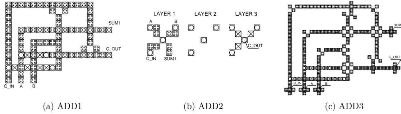
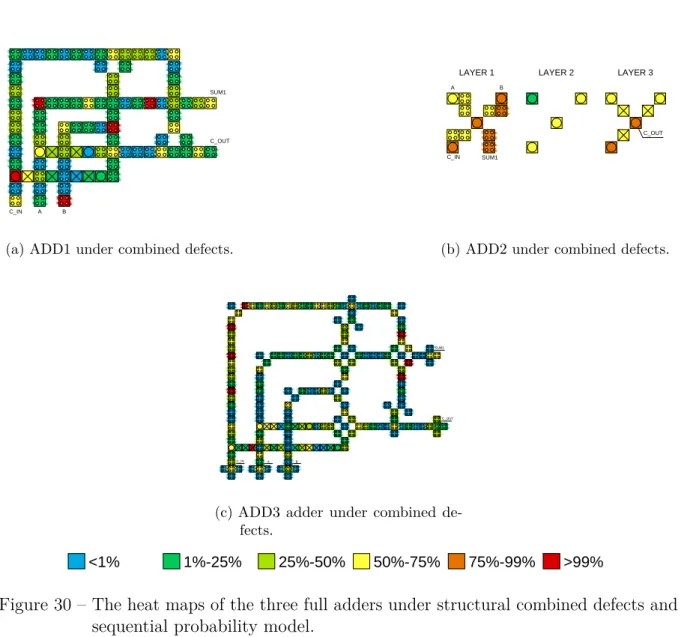
Figure 29 – The three full adders submitted to structural defects testing. . . 67
Figure 30 – The heat maps of the three full adders under structural combined defects and sequential probability model. . . 68
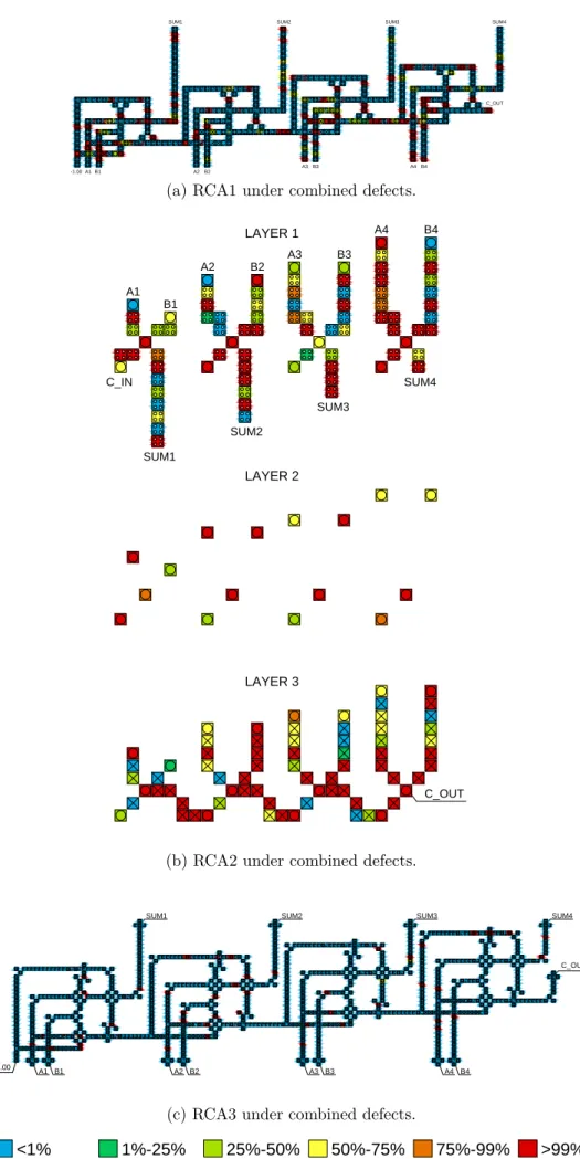
Figure 31 – The three RCAs submitted to structural defects testing. . . 70
Figure 32 – The heat maps of the three RCAs under structural combined defects and uniform probability model. . . 73
Figure 33 – WIR1 under individual defect classes . . . 99
Figure 34 – BWI1 under individual defect classes . . . 99
Figure 35 – FO21 under individual defect classes . . . 100
Figure 36 – FO31 under individual defect classes . . . 101
Figure 37 – WIR1 and WIR2 under combined defects . . . 103
Figure 38 – BWI1 and BWI2 under combined defects . . . 103
Figure 39 – FO21 and FO22 under combined defects . . . 104
Figure 40 – FO31 and FO32 under combined defects . . . 104
Figure 41 – INV1, INV2 and INV3 under combined defects . . . 105
Figure 42 – MAJ1, MAJ2 and MAJ3 under combined defects . . . 106
Figure 43 – ADD1, ADD2 and ADD3 under combined defects . . . 107
List of Tables
Table 1 – List of the available Error Analysis Module parameters that should be set through the specific window, along with its corresponding ranges and
units . . . 40
Table 2 – Comparison between error-free simulations rate for regular and modified fundamental components. . . 54
Table 3 – Average error-free simulations rate for QCA fundamental components under synchronous and asynchronous clocking schemes . . . 59
Table 4 – The results of one characterization round for three types of NOT gates under random defects from the four defect classes combined. . . 62
Table 5 – The results of one characterization round for three types of 3-input majority gates under random defects from the four defect classes combined. 64 Table 6 – The results of one characterization round for three types of full adders under random defects from the four defect classes combined. . . 67
Table 7 – The results of one characterization round for three types of RCAs under random defects from the four defect classes combined. . . 71
Table 8 – Error-free Simulations Rates - Individual Defect Classes . . . 98
Table 9 – Error-free Simulations Rates - Combined Defect Classes . . . 102
Table 10 – Error-free percent for wire under dislocation defects . . . 108
Table 11 – Error-free percent for wire under dopant defects . . . 109
Table 12 – Error-free percent for wire under interstitial defects . . . 110
Table 13 – Error-free percent for wire under vacancy defects . . . 111
Table 14 – Error-free percent for bend wire under dislocation defects . . . 112
Table 15 – Error-free percent for bend wire under dopant defects . . . 113
Table 16 – Error-free percent for bend wire under interstitial defects . . . 114
Table 17 – Error-free percent for bend wire under vacancy defects . . . 115
Table 18 – Error-free percent for fanout of 2 under dislocation defects . . . 116
Table 19 – Error-free percent for fanout of 2 under dopant defects . . . 117
Table 20 – Error-free percent for fanout of 2 under interstitial defects . . . 118
Table 21 – Error-free percent for fanout of 2 under vacancy defects . . . 119
Table 22 – Error-free percent for fanout of 3 under dislocation defects . . . 120
Table 23 – Error-free percent for fanout of 3 under dopant defects . . . 121
Table 24 – Error-free percent for fanout of 3 under interstitial defects . . . 122
Table 25 – Error-free percent for fanout of 3 under vacancy defects . . . 123
Table 26 – Error-free percent for inverter under dislocation defects . . . 124
Table 27 – Error-free percent for inverter under dopant defects . . . 125
Table 29 – Error-free percent for inverter under vacancy defects . . . 127
Table 30 – Error-free percent for 3-input majority gate under dislocation defects . . 128
Table 31 – Error-free percent for 3-input majority gate under dopant defects . . . . 129
Table 32 – Error-free percent for 3-input majority gate under interstitial defects . . 130
Table 33 – Error-free percent for 3-input majority gate under vacancy defects . . . 131
Table 34 – Error-free percent for full adder under dislocation defects . . . 132
Table 35 – Error-free percent for full adder under dopant defects . . . 133
Table 36 – Error-free percent for full adder under interstitial defects . . . 134
Table 37 – Error-free percent for full adder under vacancy defects . . . 135
Table 38 – Error-free percent for 4-Bit Ripple-carry adder under combined defects . 136 Table 39 – Error-free simulation rates for QCA wires with phase-deviated syn-chronous clock signals (α = 0 %). . . 140
Table 40 – Error-free simulation rates for QCA wires with phase-deviated asyn-chronous clock signals (α = 10 %). . . 141
Table 41 – Error-free simulation rates for QCA wires with phase-deviated asyn-chronous clock signals (α = 20 %). . . 142
Table 42 – Error-free simulation rates for QCA wires with phase-deviated asyn-chronous clock signals (α = 30 %). . . 143
Table 43 – Error-free simulation rates for QCA wires with phase-deviated asyn-chronous clock signals (α = 40 %). . . 144
Table 44 – Wire - Error-free rates . . . 145
Table 45 – Error-free simulation rates for QCA bend wires with phase-deviated synchronous clock signals (α = 0 %). . . 147
Table 46 – Error-free simulation rates for QCA bend wires with phase-deviated asynchronous clock signals (α = 10 %). . . 148
Table 47 – Error-free simulation rates for QCA bend wires with phase-deviated asynchronous clock signals (α = 20 %). . . 149
Table 48 – Error-free simulation rates for QCA bend wires with phase-deviated asynchronous clock signals (α = 30 %). . . 150
Table 49 – Error-free simulation rates for QCA bend wires with phase-deviated asynchronous clock signals (α = 40 %). . . 151
Table 50 – Bend wire - Error-free rates . . . 152
Table 51 – Error-free simulation rates for QCA Fanout of 2 with phase-deviated synchronous clock signals (α = 0 %). . . 154
Table 52 – Error-free simulation rates for QCA Fanout of 2 with phase-deviated asynchronous clock signals (α = 10 %). . . 155
Table 54 – Error-free simulation rates for QCA Fanout of 2 with phase-deviated asynchronous clock signals (α = 30 %). . . 157 Table 55 – Error-free simulation rates for QCA Fanout of 2 with phase-deviated
asynchronous clock signals (α = 40 %). . . 158 Table 56 – Fanout of 2 - Error-free rates . . . 159 Table 57 – Error-free simulation rates for QCA Fanout of 3 with phase-deviated
synchronous clock signals (α = 0 %). . . 161 Table 58 – Error-free simulation rates for QCA Fanout of 3 with phase-deviated
asynchronous clock signals (α = 10 %). . . 162 Table 59 – Error-free simulation rates for QCA Fanout of 3 with phase-deviated
asynchronous clock signals (α = 20 %). . . 163 Table 60 – Error-free simulation rates for QCA Fanout of 3 with phase-deviated
asynchronous clock signals (α = 30 %). . . 164 Table 61 – Error-free simulation rates for QCA Fanout of 3 with phase-deviated
List of abbreviations and acronyms
CMOS Complementary Metal-Oxide Semiconductor
QCA Quantum-Dot Cellular Automata
MQCA Molecular Quantum-Dot Cellular Automata
NML Nanomagnet Logic
SOI Silicon-on-insulator
RCA Ripple Carry Adder
Contents
1 INTRODUCTION . . . . 1
1.1 Motivation . . . 1 1.2 Contributions . . . 2 1.3 The thesis roadmap . . . 3 1.4 Definitions . . . 3
2 BACKGROUND . . . . 5
2.1 Quantum-dot Cellular Automata . . . 5
2.1.1 QCA Cells. . . 5 2.1.2 Principle . . . 6 2.1.3 Structures . . . 9 2.1.4 QCA Clocking . . . 10 2.1.5 QCADesigner Simulation Tool . . . 13
2.1.5.1 Bistable Engine . . . 14 2.1.5.2 The Coherence Vector Engine . . . 15
2.1.6 QCA Types . . . 16
2.1.6.1 Metal-island. . . 16 2.1.6.2 Semiconductor . . . 17 2.1.6.3 Molecular . . . 18 2.1.6.4 Magnetic . . . 19
2.2 Robustness . . . 20
2.2.1 QCA Defects Modeling . . . 20 2.2.2 QCA Clocking Phases Shifts Modeling . . . 22
3 RELATED WORKS . . . 23
3.1 QCA Defect-Tolerant Structures . . . 23 3.2 Methodologies for Error Analysis in QCA Structures . . . 26 3.3 QCA Robust Clocking Circuits . . . 28 3.4 Methodology for Error Analysis in Phase-shifted Clock Signals . . . 29
4 QCA DEFECTS SIMULATOR . . . 31
4.1 Methodology . . . 31
4.1.1 Initial procedures . . . 32 4.1.2 Intermediate procedures . . . 36 4.1.3 Final procedures . . . 38
4.2.1 Error analysis module interfaces . . . 38
4.3 Presenting the Results . . . 41
4.3.1 The Result File . . . 42 4.3.2 The Heat Maps . . . 43
5 STRATEGIES FOR ROBUSTNESS ENHANCEMENT . . . 45
5.1 QCA Fundamental Components under Structural Defects . . . 45
5.1.1 Components Selection . . . 45 5.1.2 Testing Settings. . . 46 5.1.3 Qualitative Analysis of Heat maps . . . 48 5.1.4 Strengthen Strategies . . . 52 5.1.5 Regular × Modified Components. . . 53
5.2 QCA Fundamental Components under Phase-Shifted Clock Signals 55
5.2.1 Testing Settings. . . 55 5.2.2 Qualitative Analysis of Waveforms . . . 56 5.2.3 Asynchronous Clocking Scheme . . . 57 5.2.4 Synchronous × Asynchronous Clocking Schemes . . . 58
6 ROBUST QCA CIRCUITS AND SYSTEMS . . . 61
6.1 Inverter . . . 61 6.2 3-input Majority . . . 63 6.3 Full Adder . . . 66 6.4 4-bit Ripple-carry Adders . . . 69 6.5 Discussion . . . 71
7 CONCLUSIONS . . . 75
BIBLIOGRAPHY . . . 79
APPENDIX
87
APPENDIX B – SIMULATION RESULTS - STRUCTURAL DE-FECTS . . . 97 B.1 Sequential Probability Model Tests . . . 98
B.1.1 Individual Defect Classes . . . 98
B.1.1.1 Error-free Simulations Rates . . . 98 B.1.1.2 Heat Maps . . . 99
B.1.2 Combined Defect Classes . . . 102
B.1.2.1 Error-free Simulations Rates . . . 102 B.1.2.2 Heat Maps . . . 103
B.2 Uniform Probability Model Tests . . . 108
B.2.1 Wire . . . 108
B.2.1.1 Dislocation defects. . . 108 B.2.1.2 Dopant defects . . . 109 B.2.1.3 Interstitial defects . . . 110 B.2.1.4 Vacancy defects . . . 111
B.2.2 Bend Wire . . . 112
B.2.2.1 Dislocation defects. . . 112 B.2.2.2 Dopant defects . . . 113 B.2.2.3 Interstitial defects . . . 114 B.2.2.4 Vacancy defects . . . 115
B.2.3 Fanout of 2 . . . 116
B.2.3.1 Dislocation defects. . . 116 B.2.3.2 Dopant defects . . . 117 B.2.3.3 Interstitial defects . . . 118 B.2.3.4 Vacancy defects . . . 119
B.2.4 Fanout of 3 . . . 120
B.2.4.1 Dislocation defects. . . 120 B.2.4.2 Dopant defects . . . 121 B.2.4.3 Interstitial defects . . . 122 B.2.4.4 Vacancy defects . . . 123
B.2.5 Inverter . . . 124
B.2.5.1 Dislocation defects. . . 124 B.2.5.2 Dopant defects . . . 125 B.2.5.3 Interstitial defects . . . 126 B.2.5.4 Vacancy defects . . . 127
B.2.6 3-input Majority gate . . . 128
B.2.6.4 Vacancy defects . . . 131
B.2.7 Full Adder . . . 132
B.2.7.1 Dislocation defects. . . 132 B.2.7.2 Dopant defects . . . 133 B.2.7.3 Interstitial defects . . . 134 B.2.7.4 Vacancy defects . . . 135
B.2.8 4-Bit Ripple-carry Adder . . . 136
B.2.8.1 Combined defects . . . 136
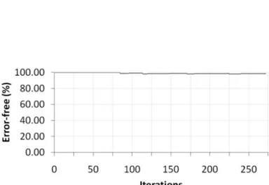
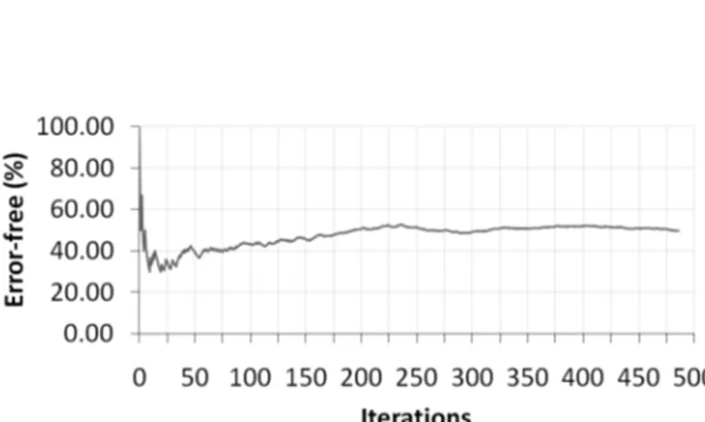
B.2.8.1.1 Heat maps . . . 137 B.2.8.1.2 Error-free percent x Iterations . . . 138
APPENDIX C – SIMULATION RESULTS - PHASE-SHIFTED CLOCK SIGNALS . . . 139 C.1 Wire . . . 140
C.1.1 Synchronous clock signals (α= 0 %) . . . 140 C.1.2 Asynchronous clock signals (α = 10 %) . . . 141 C.1.3 Asynchronous clock signals (α = 20 %) . . . 142 C.1.4 Asynchronous clock signals (α = 30 %) . . . 143 C.1.5 Asynchronous clock signals (α = 40 %) . . . 144
C.2 Bend Wire . . . 147
C.2.1 Synchronous clock signals (α= 0 %) . . . 147 C.2.2 Asynchronous clock signals (α = 10 %) . . . 148 C.2.3 Asynchronous clock signals (α = 20 %) . . . 149 C.2.4 Asynchronous clock signals (α = 30 %) . . . 150 C.2.5 Asynchronous clock signals (α = 40 %) . . . 151
C.3 Fanout of 2 . . . 154
C.3.1 Synchronous clock signals (α= 0 %) . . . 154 C.3.2 Asynchronous clock signals (α = 10 %) . . . 155 C.3.3 Asynchronous clock signals (α = 20 %) . . . 156 C.3.4 Asynchronous clock signals (α = 30 %) . . . 157 C.3.5 Asynchronous clock signals (α = 40 %) . . . 158
C.4 Fanout of 3 . . . 161
1
1 Introduction
1.1
Motivation
Complementary Metal-Oxide Semiconductor (CMOS) technology has been widely used for the realization of integrated circuits since the late sixties (HOEFFLINGER, 2012). The vast knowledge of its manufacturing process as well as the application of the scaling theory allowed a remarkable increment in the devices integration density (BROWN et al., 2004). Practical observations of the amount of transistors in a single chip has endorsed the predictions of Moore (1965). However, despite the advantages, scaling has resulted in some severe problems such as power consumption and reliability concerns (ITRS, 2004). As the feature-size decreases, quantum effects and current leakage becomes more significant thereby promoting the increment of the static power consumption (FRANK, 2002). The large-scale integration of the devices causes a huge demand for thermal dissipation that are not always possible to meet, resulting in reliability losses. The alarming situation may lead to the discontinuity of the scaling process in a short-medium term, which encourages the rising of new nanotechnologies that enable the continuity of the feature size reduction (KAUR et al., 2015). The Beyond Moore terminology is associated to the new nanotechnology devices that will emerge as possible CMOS successors (HUTCHBY et al., 2002).
Quantum-Dot Cellular Automata (QCA) is among the promising emerging nan-otechnologies that aim to solve the challenges faced by CMOS. The QCA operation principle takes advantage of the quantum mechanical phenomena to transport the infor-mation and perform logic operations without electric current flow, which implies in a low power consumption (LENT et al., 1993). A very high packing density may be achieved, since each cell is in the range of a few nanometers. However, QCA has to overcome several challenges before its consolidation (SAHNI, 2008). Undoubtedly, the most worrisome one is the extremely difficult physical implementation. High-resolution lithography techniques has been developed in order to eventually enable the fabrication of molecular QCA (HU et al., 2005). Prototypes of Metal-Island QCA and NML (Nanomagnetic Logic) devices have been successfully implemented as reported in (TóTH; LENT, 1999) and in (ALAM, 2010). However, none of the QCA realizations surpassed the performance of their CMOS counterparts so far.
2 Chapter 1. Introduction
or to the pronounced effect of the manufacturing process variability, more likely to occur in nanoscale (HARON; HAMDIOUI, 2008). The creation of methodologies for error analysis as well as the proposal of robustness enhancing techniques for structures and information sequencing are mandatory steps towards the consolidation of the QCA nanotechnology (DYSART, 2009).
1.2
Contributions
This thesis introduces a QCA Defects simulator, implemented according to the precepts of a novel methodology for error analysis. The tool allows the robustness analysis of QCA structures under several classes of defects inserted into the cells or in the clock signals. The effect of defective elements to a structure expected behavior is evaluated and the results are presented by means of tables and heat maps. This graphical tool uses a color range in order to highlight the defective cells that are more likely to cause errors to the outputs.
Furthermore, the work describes robustness enhancing strategies for both the arrangements of cells that might contain defective elements and the clocking circuits, which comprise the timing synchronization mechanisms regarding QCA.
The polarization strengthen techniques comprises changes in the positioning, along with the addition of cells to specific regions of the structure. The additional cells strength the Coulomb interactions and increase the resilience to defects, as reported by Dysart, Lohmer and Kogge (2008). Two distinct scenarios are analyzed for the robustness enhancement. In the first one, thick wires (DYSART, 2003) are used to surround all the structure with extra devices, thereby promoting the robustness enhancement through redundancy. The impact on the robustness is evaluated, as well as the possible creation of secondary effects as the increment in the number of cells and response time. A similar procedure is employed to analyze the results of the tests in the second scenario, where QCA Defects simulator is previously used in order to identify the weakest regions of the same structure. Once the weaknesses are identified, the strengthen technique is applied only to those regions.
1.3. The thesis roadmap 3
Finally, the robustness-enhanced structures obtained with the aim of the QCA Defects Simulator are employed in order to design four circuits of gradual levels of complexity, i.e.an inverter (TOUGAW; LENT, 1994), a three-input majority gate adapted from (TOUGAW; LENT, 1994), a full adder and a ripple carry adder adapted from (BRUSCHI et al., 2011). The use of the strengthen technique creates redundant mechanisms for information propagation with a reduced increment in the number of cells in a structure, compared to the indiscriminate use of thick wires.
1.3
The thesis roadmap
This master thesis is organized into seven chapters, including this Introduction. The remaining chapters are outlined below.
Chapter 2 is entitled Background and divided into two main sections. The first section of Chapter 2 introduces the concepts of the QCA nanotechnology, while its second section presents the general aspects of robustness, later focusing on the QCA context.
Chapter 3, Related Works, is a summary of the methodologies for error analysis in the nanotechnology QCA that has been previously reported in the literature.
Chapter 4 is entitled QCA Defects Simulator. Its first section discusses a novel methodology for error analysis in defective circuits. Its second section presents the imple-mentation of such methodology as an extension to an existing simulation tool. Finally, its third section discusses the resources used for presenting the simulation results. The use of heat maps and tables make the results easier to be interpreted.
Chapter 5 defines, in its first section, strategies for robustness enhancement for both cell-defective and clock-defective circuits. The robust structures designed by means of such strategies are presented in the second and third sections.
Chapter 6 presents the designs and simulation results of four logic circuits where the techniques for robustness enhancement are applied, i.e.an inverter (TOUGAW; LENT, 1994), a three-input majority gate adapted from (TOUGAW; LENT, 1994), a full adder and a ripple carry adder adapted from (BRUSCHI et al., 2011).
Chapter 7 concludes the work and presents suggestions for future works.
1.4
Definitions
This section defines some key terms often used along the thesis.
• Device: The fundamental building block of an electronic system. For instance,
4 Chapter 1. Introduction
• Structure: Any arrangement of devices. Comprises all the categories defined below:
Fundamental and logic components, circuits and systems.
• Fundamental Component: An arrangement of devices designed under the
pur-pose of transporting and distributing information within a logic component/circuit or interconnect different circuits into a system, i.e. wires and fan outs.
• Logic Component: An arrangement of devices designed to implement an elemental
logic function, i.e. the logic gates.
• Circuit: A collection of components combined together in order to perform a
com-plex logic function, i.e. full adders, multiplexers and memory cells.
• System: A set of circuits interconnected in order to process a higher level function,
i.e. Ripple Carry Adders (RCAs), processors, routers, memory architectures and ALUs (Arithmetic Logic Units).
• Defect: In the context of this work, defects are flaws of the cells of a structure,
generally caused by manufacturing process variations.
• Errors:Errors, in this work, are unexpected deviations in the behavior of the system.
In the circuit’s context, an error occurs when, given a known input vector, the state of the outputs is unexpected.
• Robustness: Robustness, in the context of this work, may be defined as the system
capability to get along with defects and operate under unusual conditions.
• Defect-Tolerance: The terms robustness and defect-tolerance here are
interchange-able. That is, a defect-tolerant system possess good resilience to defects.
• Characterization Round: The term is applied to denote one complete execution
5
2 Background
This chapter introduces the essential concepts to the better understanding of this work. Its contents are divided into two major sections. The first one, entitled Quantum-Dot Cellular Automata, elucidates the basics regarding QCA. The second major section focuses on the concepts of robustness and defect tolerance, in both general and particular contexts.
2.1
Quantum-dot Cellular Automata
Quantum-Dot Cellular Automata (QCA) is a new computation paradigm described by Lent et al. (1993) in which the information transport and processing occur by means of Coulomb interactions rather than electric current flow, enabling a low power consumption. QCA devices have dimensions of few nanometers and are expected to operate at speeds within the range of Terahertz (KIM; WU; KARRI, 2006). QCA is considered one of the promising emerging nanotechnologies candidate for CMOS succession (ITRS, 2004).
2.1.1 QCA Cells
A QCA cell is the most fundamental device of the nanotechnology QCA. It comprises four or five nanometer-sized quantum dots, in which electrons may be confined. Due to their unique electronic and optical properties, quantum dots have a range of applications besides the construction of the QCA cells. For instance, they can be used to implement single-electron transistors, tunable lasers, solar cells and photo detectors (ALFEROV, 2001). Some atomic force microscopy images of quantum dots are depicted in Figure 1.
(a) An InAs quantum dot structure grown on GaAs substrate (NSTC, 1999).
(b) The quantum dot shape may vary depending on the process and application requirements (LIANG; XIE, 2015).
6 Chapter 2. Background
The four-dot QCA cell model is depicted by Figure 2a. As introduced by (LENT; TOUGAW, 1997), it comprises four circles, which represent the quantum dots, strategically positioned at the internal corners of a square-shaped substrate. Two electrons are hold trapped into those structures due to the very high inter-dot potential barriers. According to the Coulomb repulsion effect, the electrons must be as far apart as possible. Consequently, there are two possible logic states (opposite diagonals), which permits a binary logic. By convention, the maximum polarization states, which correspond respectively to logic 0 and logic 1, are called -1 and +1. A cell can continuously assume any polarization level within those limits. Figure 2b depicts the two possible interpretations for the cell logic state, which depends on the comparison between the threshold and the polarization level.
(a) The representation of a four-dot QCA cell. (b) The QCA cell logic state interpretation
de-pends on the threshold of the polarization level. In the figure, a fulffiled circle represents a trapped electron.
Figure 2 – A QCA cell and its two possible logic states
2.1.2 Principle
As exposed in Section 2.1.1, a cell carries its individual information, which comprises its logic state along with the corresponding polarization level. It is possible to propagate such information along a path to an output through a cells arrangement. The same quantum mechanical phenomena, that explains the positioning of the two trapped electrons at the opposite diagonals of a cell, is responsible for the two-way electrostatic interactions between two or more cells within a common radius of influence (LENT; TOUGAW, 1997).
Whereas initially the cells on the path are at their ground states, a cost of energy, defined as Kink Energy (Ek), is required in order to provoke changes in their individual polarization levels so that the information is propagated to the outputs (TOUGAW; LENT, 1996). As shown in (DYSART, 2009), Ek is computed as the difference between the two-way electrostatic interactions of two adjacent cells (i andj) whereas they have either the oppositeEdif f
i,j or the same Esamei,j polarization levels (2.1).
2.1. Quantum-dot Cellular Automata 7
In order to find the terms of the difference of the equation (2.1), the two-way electrostatic interaction between the dots of both cells —whose width and length, in nanometers, are expressed in terms of the letter L —are calculated and summed over all i and j according to (2.2).
Ei,j =
3
X
ni=0
3
X
nj=0 1 4πǫ0ǫr
qniqnj
|rni−rnj| (2.2)
Where:
Ei,j : Amount of energy for the cells i and j having any polarization levels ni : Index of the dots in cell i
nj : Index of the dots in cell j
ǫ0 : The permittivity of the free space (For the vacuum it is 8.8545 x 10¹² F/m)
ǫr : The relative permittivity of the material system (For a GaAs/AlGaAs cell it is roughly 12.9)
qni : The electronic charge located on dot ni (The elementary charge is 1.6022 x 10⁻¹⁹ C)
qnj : The electronic charge located on dot nj (The elementary charge is 1.6022 x 10⁻¹⁹ C)
|rni−rnj|: The distance between the dots ni and nj
By replacing the appropriate values for the constants along with the interdots distances, it is possible to calculate the energies Edif f and Esame whether the cells i and j are placed in line or in diagonal as depicted in the Figure 3.
(a) Cells i and j positioned in line. (b) Cells i and j positioned in diagonal.
Figure 3 – Two different arrangements for the cells i and j. A fulfilled dot represent a trapped eletron. The polarization of the cell i is arbitrarily established as +1.
8 Chapter 2. Background
Esame=
3 X ni=0 3 X nj=0 1 4πǫ0ǫr
qniqnj |rni−rnj| =
1.6022×10⁻¹⁹
C2
4×π×8.8545×ǫr×1012F/m×
1 1.0000 + 1 0.7071 + 1 1.0000 + 1 1.5811× × 1
10−9m×L
Esame= 2.3019×10−521
ǫr C2
m V ×
4.0467×10⁹
m−1
L
!
Esame= 9.3151×10−43 1
ǫr×LJ
Edif f =
3
X
ni=0
3
X
nj=0 1 4πǫ0ǫr
qniqnj |rni−rnj| =
1.6022×10⁻¹⁹
C2
4×π×8.8545×ǫr×1012F/m×
1 0.5000 + 1 0.9014 + 1 0.9014 + 1 1.5000 × 1
10−9m×L
Edif f = 2.3019×10−521
ǫr C2
m V ×
4.8855×10⁹
m−1
L
!
Edif f = 1.1246×10−42 1
ǫr×LJ
Likewise, for the cells i and j placed in diagonal as depicted in Figure 3b, the energiesEsame and Edif f may be calculated as follows:
Esame=
3
X
ni=0
3
X
nj=0 1 4πǫ0ǫr
qniqnj |rni−rnj| =
1.6022×10⁻¹⁹
C2
4×π×8.8545×ǫr×1012F/m×
1 1.4142 + 1 0.7071 + 1 1.4142 + 1 2.1213 × 1
10−9m×L
Esame= 2.3019×10−521
ǫr C2
m V ×
3.2998×10⁹
m−1
L
!
Esame= 7.5958×10−43 1
ǫr×LJ
Edif f =
3
X
ni=0
3
X
nj=0 1 4πǫ0ǫr
qniqnj |rni−rnj|
= 1.6022×10
−19
C2
4×π×8.8545×ǫr×1012F/m×
1 1.1180 + 1 1.8022 + 1 1.1180 + 1 1.8022 × 1
10−9m×L
Edif f = 2.3019×10−521
ǫr C2
m V ×
2.8983×10⁹
m−1
L
!
Edif f = 6.6716×10−43 1
ǫr×LJ
2.1. Quantum-dot Cellular Automata 9
to the equation 2.2 as 1.1246×10−42 1
ǫr×LJ. Such value is substantially higher than the
energy of 9.3151×10−43 1
ǫr×LJ required for the cells having the same polarization (E
same), computed similarly to Edif f by means of the equation 2.2. Since any electrostatic system tend to the ground, which is the state of less energy, aligned cells are likely to have same polarization. Thus, QCA arrays of aligned cells usually perform the function to propagate information forward in a structure (TOUGAW; LENT, 1996).
On the other hand, for the diagonal arrangement of the cells i and j depicted in Figure 3b, the value obtained for Edif f,Ek
i,j = 6.6716×10−43ǫr1×LJ, is slightly lower than
the amount of energy Esame, computed as 7.5958×10−43 1
ǫr×LJ. Therefore, for the same
reasons aforementioned in the previous paragraph, diagonally positioned cells are likely to have opposite polarization. Thus, QCA cells placed in diagonals usually play the role to successive invert the logic state through a QCA array (TOUGAW; LENT, 1996).
Therefore, the transmission and processing of information in QCA are based on the principle of the Kink Energy, which is a consequence of the electrostatic interaction guided by the Coulomb’s Law. Two or more cells positioned in a row are able to transmit a logic state from an input to an output. Moreover, cells positioned in diagonal successive invert the logic state through a QCA arrangement.
2.1.3 Structures
Due to the principle previously explained in the section 2.1.2, QCA cells may be arranged to transmit information and perform computation. In this work, any arrangement of cells, regardless of its primary purpose, is generally called as a structure. QCA structures, in turn, may be categorized into fundamental/logical components, circuits or systems, according to the definitions of the Section 1.4.
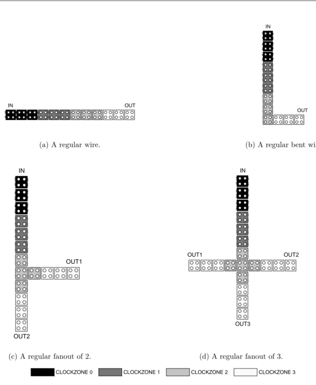
Some of the first QCA structures are reported in the literature by Tougaw and Lent (1994). They are illustrated in Figure 4. There, the terms input and output refer, respectively, to the starting and to the endpoint of a arrangement of common QCA cells from the left to the right of the observer.
10 Chapter 2. Background
means of specific interface contacts placed in a layer underneath the QCA layer.
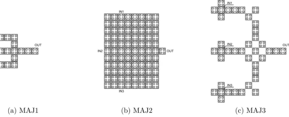
The QCA wire, depicted in the Figure 4a is responsible for sequentially propagating a logic state from one cell to the next cell, from the starting (input) to the endpoint (output). The inverter, in turn, takes advantage of a diagonally positioned cell to invert the logic state of the signal applied to the input. The inversion principle is explained in Section2.1.2. Once inverted, the signal is transmitted forward to the output. The three-input majority gate (Figure 4c) has a core cell, also known as device cell, positioned in the middle of the component, which is surrounded by other four cells in a cross-shaped disposition —three inputs and one output. The referred core cell is responsible for performing the computation, once it is likely to assume the same logic state present at the majority of its inputs and propagate it to the output. The majority gate is considered, along with the inverter, the most basic logical components in QCA, since any logic can be created from them (TOUGAW; LENT, 1994). For instance, two circuits which perform more complex logic functions, the XOR gate and the full adder depicted in the Figures 4d and 4e, have many of wires, inverters, majority gates and further components built-in within their structures.
The researchers are always looking forward to create innovative QCA designs. Thus, more than two decades later from the initial proposal, different approaches have been emerging in order to improve the architecture of the QCA components and circuits. For instance, some robust components and circuits have been being proposed, as thick wires ((DYSART, 2003) (DYSART; LOHMER; KOGGE, 2008)), thick co-planar cross-ings ((BHANJA et al., 2007)), inverters (BEARD, 2006), majority gates (FARAZKISH; SAYEDSALEHI; NAVI, 2012) (ROOHI et al., 2014) and full adders (SAFAVI; MOSLEH, 2013) (FARAZKISH, 2015) (ROOHI; DEMARA; KHOSHAVI, 2015). Furthermore, the emerging of new QCA systems, able to perform more complex tasks have been reported in the literature, as memories (SARDINHA et al., 2015) (ANGIZI et al., 2015) , processors (WALUS et al., 2005) (FAZZION et al., 2014) and a router (SILVA et al., 2015).
2.1.4 QCA Clocking
The operation of the QCA structures is highly dependent on a synchronous infor-mation flow (OTTAVI et al., 2007). Therefore, the designer must ensure that all the inputs of the logical components or circuits are driven at the same time by the fundamental components. Otherwise, a wrong logic processing is likely to happen. Such event may lead the structure to produce erroneous logic states, which implies in severe concerns on its robustness.
2.1. Quantum-dot Cellular Automata 11
the quantum dots of a cell may switch their configuration to the opposite diagonal by tunneling. The transition leads the cell to a change between the two logic states thus its polarization. Such process shall occur in an adiabatic manner, by gradually adjusting the level of the inter-dot potential barriers in order to allow or deny the electron tunneling. Suddenly changes in the polarization level should be avoided, as they can lead the system to reach a metastable state that may cause undesirable delays or wrong logic processing (LANDAUER, 1994).
(a) A wire. (b) An inverter.
(c) A three-input majority gate. (d) A XOR.
(e) A full adder.
12 Chapter 2. Background
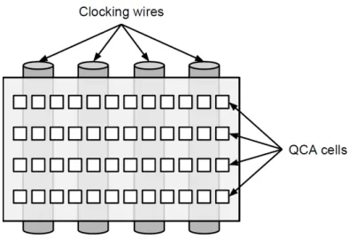
External signals should control the devices adiabatic switching in each clock zone. Those signals are called clock signals, which are provided by an external clock circuit. Interconnects of such external circuit should be positioned underneath the QCA layer, being able to deliver the clock signal to every cell in the system. The inter-dot potential barrier control occurs by means of the interactions between the cells electrical field and its counterpart created by the flow of the clock signals through the interconnects. A possible placement of the clock circuit within a QCA system is illustrated in Figure 5. Metallic clock wires should be placed according to a specific clocking scheme, which is a predefined pattern that aims to address the clock signals to the respective clock zones. Some examples of clocking schemes may be found in (VANKAMAMIDI; OTTAVI; LOMBARDI, 2008) and (CAMPOS et al., 2015).
Figure 5 – Interconnects from the external clock circuit, i.e. clocking wires, underneath the QCA layer (CAMPOS, 2015).
A clock signal has four sequential phases: Switch, hold, release and relax (LENT; TOUGAW, 1997). The inter-dot barriers of a cell are differently managed in each phase in order to allow or deny the electron tunneling thus changes in the polarization level. The conventional approach for the clocking design is to provide synchronous clock signals, i.e. each phase have an individual time ofπ/4 radians, which corresponds to a quarter of the clock signal period.
Figure 6 depicts the general behavior of the inter-dot potential barriers level associated to the clock phases.
2.1. Quantum-dot Cellular Automata 13
Figure 6 – The cell inter-dot potential barrier behavior at the four distinct clock phases.
In the hold phase, the inter-dot potential barriers are kept at the highest level achieved in the previous (switch) phase, so the cell is insusceptible to external influences despite the electrostatic interactions between itself and its neighbors.
In the release phase, the inter-dot potential barriers are linearly lowered from the highest to the lowest level possible. At this time the cell is able to depolarize. After the end of the depolarizing process, a cell shall not carry remainder polarization.
At last, in the hold phase, the inter-dot potential barriers are kept at the lowest level achieved in the previous (release) phase, so the cell remains depolarized until a new cycle restarts at the switch phase.
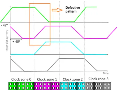
The cells of a QCA system are usually grouped into sequential sub sections, most known as zones. A single clock signal is applied in order to synchronize the polarization change process of all the cells within a zone. In the traditional clocking distribution model, the clock signal of a zone is naturally phase-shifted in relation to its counterpart of the adjacent zone, as depicted in Figure 7. The phase shift P for the clock signals in the traditional model is given by the relation: P = (π/2)×i, wherei is a sequential zone identifier: 0 ≤ i ≤ 3. The identification scheme for clocking zones is cyclic, that is, the clocking zone 2 is succeeded by the clocking zone 3, which in turn precedes the clocking zone 0 that starts a new cycle. The zones arrangement in QCA circuits enables the information transport and processing in a pipeline fashion.
2.1.5 QCADesigner Simulation Tool
14 Chapter 2. Background
Figure 7 – A QCA wire divided into four zones and their respective clock signals (depicted in the same colors). The phase shifts are indicated next to the graphs.
into that simulation tool, which was devised according to the precepts of USE, a novel QCA clocking scheme (CAMPOS, 2015). The most recent official release of QCADesigner, the version 2.0.3, was launched in 2009.
One of the most important aspects of the QCADesigner is that such tool allows an user to quickly layout a QCA design and determine its functionality by means of two efficient simulation approaches —The Bistable and the Coherence Vector engines —which are introduced on the following subsections.
2.1.5.1 Bistable Engine
In the Bistable engine, each cell is modeled as a simple two-state system, described by the Hamiltonian Matrix 2.3.
Hi =
−1 2PjE
k
i,j −γ
−γ 1
2PjE
k i,j
(2.3)
Where:
Pj : Polarization of the cell j Ek
i,j : Kink energy between cells i and j
γ : Tunneling energy between the eletrons in the cell, which is controlled by the clock signal
2.1. Quantum-dot Cellular Automata 15
within an radius of effect i. Within the QCADesigner tool, the neighborhood, i.e. the radius of effect of one cell to another, is defined by a specific parameter for both Bistable and Coherence Vector engines. The polarization of each cell is computed until the whole circuit converges to the ground state, which is defined by means of a preset of tolerance.
The Bistable engine is efective to simulate large circuits in a short amount of time. Thus, it has been serving as the foundation for the majority of the QCA works that has been done so far (LIU; O’NEILL; SWARTZLANDER, 2013). However, this method does not consider the most complete version of the Hamiltonian, since it ignores the quantum correlations within and between cells. Thus, the price of this relatively quick computation is inaccuracy regarding the QCA dynamics, as the bistable engine undermines the intercellular entanglement, which sometimes causes incorrect logic states at the outputs of the circuits.
A more accurate time-dependent engine —The Coherence Vector —is also available within the QCADesigner. Such engine is described in the next subsection.
2.1.5.2 The Coherence Vector Engine
The Coherence Vector engine, which principle is based on deculping the two-way cells interactions by using the density matrix approach, is adopted to describe the two-way interactions between devices within and among QCA structures. Such engine is considered as the most accurate among the two options included in the tool QCADesigner version 2.0.3, since it allows a time-dependent analysis, also taking into account power dissipation effects (LIU; O’NEILL; SWARTZLANDER, 2013). The Coherence Vector concept and formalism are briefly described in the following.
Much as to that described for the Bistable engine, in the devices model devised for the Coherence Vector each cell is considered as a simple two-state system which can be also described by the Hamiltonian matrix (2.3). Background positive elementary charges (+1
2e) are included within the dots, so that they are taken into account for the cost of
energy Ek
i,j calculation, helping at the establishment of the electronic balance of the QCA devices. Thus, the Hamiltonian matrix depends both on the Kink Energy as on the distance between two neighbor cells, represented by the variable Ωi. The model also consider the radius of effect i and the variable γi, which is the vector form of the density matrix of one cell, i.e. the coherence vector−→λ, whose representation in motion can be described as follows (2.4).
δ−→λ δt =
− →
Γ ×−→λ − 1 τ
−→
λ −−λss→ (2.4)
16 Chapter 2. Background
Its value depends strongly on the environment, i.e. the QCA physical realization type. Alongside, the variable−λss→refers to the steady state coherence vector. The whole formalism behind the development of−→Γ and−λss, as well as a more detailed description of all elements→ in the equations may be found in (LIU; O’NEILL; SWARTZLANDER, 2013).
The coherence vector for each cell is calculated through a time-marching algorithm. The −→Γ and−λss→ values are evaluated and stepped forward in time. Despite the high com-plexity of the quantum mechanical equations involved makes the engine computationally costly, the Coherence Vector is considered as the most accurate approach for estimating the polarization levels of the cells in a QCA system among the two simulation engines available in the tool QCADesigner version 2.0.3. Thus, it is used for all simulations presented in this work.
2.1.6 QCA Types
This section describes the four classes proposed for QCA physical realization, highlighting their advantages and disadvantages.
2.1.6.1 Metal-island
A metal-island device was implemented in (ORLOV et al., 1997) as the first physical realization of a functional QCA cell. Aluminum islands and aluminum-oxide tunneling junctions were used in order to perform the quantum dots on an oxidized silicon substrate. Two double-dots, also known as half-cells, were used to reproduce the electrostatic interactions within a device. Such model was consisted of two pairs of vertically aligned dots, D1/D2 and D3/D4, positioned alongside each other. Four electrodes, VA/VB and VC/VD, were placed just before and after pair of dots, serving as input and output interfaces between the device and the external equipment from the experimental setup. When a push-pull voltage drop δVA = −δVB was applied to the input probes VA/VB, a consequent direct polarization appeared in D1/D2, which in turn induced a reverse polarization in D3/D4. Such induced polarization was sensed by means of the output electrodes VC/VD. The reported behavior represented a milestone for the QCA paradigm, since it has confirmed the theoretical predictions regarding the operation of the device.
2.1. Quantum-dot Cellular Automata 17
Although the implementation of metallic devices was important to proof the concept behind the QCA paradigm, the metal-island type does not seem to be a reasonable choice for the future systems, due to some key issues. For instance, extremely low temperatures, in the range of milikelvin, are required in order to enable the devices operation. Moreover, the metal-island are relatively large (about 1 micrometer in dimension) (LIU; O’NEILL; SWARTZLANDER, 2013).
2.1.6.2 Semiconductor
Standard semiconductor materials are employed in order to manufacture the most of the QCA prototypes (LIU; O’NEILL; SWARTZLANDER, 2013). Some works report successful physical implementations of QCA devices by means of the electron-beam lithography process. For instance, Perez-Martinez et al. (2007) used four metallic AlGaAs gates in order to simultaneously perform the quantum dots and the surface contacts for noninvasive voltage probing. The dots were placed on a GaAs substrate. In (MACUCCI et al., 2003), QCA cells were fabricated in the silicon-on-insulator (SOI) material system. The interaction between the input and the output double-dots was predicted by means of a simulation code. Thereafter, experimental measurements confirmed the expected behavior of the device. Finally, the interactions between neighbor devices has been investigated in (SMITH et al., 2003). The materials and manufacturing process employed to fabricate the cell, as well as its physical structure, were similar to those reported in (PEREZ-MARTINEZ et al., 2007). Even though each dot contained more than a hundred electrons, the movement of a single charge from one dot to its neighbor resulted in a field that was large enough to induce polarization changes for both the dots within the same cell and for the dots in the neighbor cells.
The lithography process has been increasingly improved over the last years due to the challenges imposed by the continuous scaling of the CMOS transistors (NEISSER; WURM, 2015). Despite the QCA semiconductor type takes some advantage on such technological improvements, the extremely reduced sizes of the cells - in the range of a few namometers - makes the state-of-art lithography unsuitable for the mass production of the QCA devices due to the extremely critic conditions of variability required for the process. Furthermore, all prototypes that have been already realized are not able to work at room temperature (LIU; O’NEILL; SWARTZLANDER, 2013). Instead, Perez-Martinez et al. (2007), Macucci et al. (2003) and Smith et al. (2003) reported their physically implemented
devices working in the range of milikelvin.
18 Chapter 2. Background
2.1.6.3 Molecular
The molecular type represents the reunion of several desirable characteristics for a QCA device: The achievement of speeds in the Terahertz range, operation at room-temperatures, cell sizes of 2nm or smaller and mass production fabrication enabled by means of the self-assembly process (LIU; O’NEILL; SWARTZLANDER, 2013).
A molecular QCA device consists in a single molecule, in which charge may tunnel be-tween specific sites. For the benefits mentioned above, the type has attracted considerable in-terest from some research groups around the world. The molecule {(η5−C5H5)F e(η5−C5H4)}4(η4 −C4)Co(η5 −C5H5)
2+, synthesized and characterized
by Jiao et al. (2003), has four ferrocene groups strategically located at the corners of a square-shaped structure. It is introduced on the theoretical chemistry study by Lu and Lent (2004) as a candidate for the molecular QCA device. The work results support that {(η5−C5H5)F e(η5−C5H4)}4(η4 −C4)Co(η5−C5H5)2+ is able to encode binary logic
states due to its bistable electronic feature. Furthermore, the study also indicates that the molecule can switch its logic state due to electrostatic interactions among its neighbors.
Besides{(η5−C5H5)F e(η5−C5H4)}4(η4−C4)Co(η5−C5H5)2+, other molecules
have been indicated as possible molecular QCA devices in (LENT; ISAKSEN; LIEBER-MAN, 2003) and (LENT; ISAKSEN, 2003). However, as pointed out by Pulimeno et al. (2013), none of them may be considered as suitable candidates for real systems, since the works have analyzed the molecules in vacuum, thus comprising ideal systems.
Moreover, there are no reports of experimental results in whose such molecules perform the function of a QCA cell. Indeed, a very reduced number of experimental attempts have been carried out in order to find a suitable molecule for the real QCA paradigm. The first part of a work performed by Li, Beatty and Fehlner (2003) introduces a novel unsymmetrical heterobinuclear, two-dot, F e−Ru candidate molecule. The charge transfer to a film of F e−Ru molecules was measured and reported in the further work (LI; FEHLNER, 2003).
2.1. Quantum-dot Cellular Automata 19
2.1.6.4 Magnetic
The Magnetic Quantum-Dot Cellular Automata has emerged as a QCA type in which the devices operate through magnetic interaction between nanoparticles rather than electrostatic interaction between trapped charges, as reported for all the other classes previously described (subsections 2.1.6.1, 2.1.6.2 and 2.1.6.3). The magnetic QCA type has been commonly referred in the literature as Nanomagnet Logic (NML). The information is encoded to a NML device due to its single domain magnetic dipole. Despite some particularities, such as the interaction class by which information is transmitted and the clocking organization, both electrostatic and magnetic cells have analogous polarization vectors. Thus, NML possess some of the most remarkably characteristics of other QCA types, as the ultra low power consumption and operation at room temperature (molecular QCA).
Several NML logical and fundamental components have been already physically realized (IMRE et al., 2006), (ORLOV et al., 2008), (VARGA et al., 2010), (PULECIO; BHANJA, 2010), (NAKATANI; NOMURA; ENDO, 2009), (NIEMIER et al., 2010). For instance, (IMRE et al., 2006) reports the first physically implemented NML logical component - a three-input majority gate, in which five 135x70x30 nm3 rectangular devices
were implemented by means of nanomagnets. The devices were placed in a cross-shape arrangement, in such a way that the central nanomagnet was surrounded by the four others. Three of the four surrounding devices represent the inputs, while the remaining nanomagnet plays the output device rule. All the possible logic states combinations were tested at the inputs of such majority gate, which yield 25 % of correct results at the output. Although it might seem a non-expressive percentage, the authors highlight that the probability of all eight nanomagnets assuming the correct orientation is less than 0.4 %, thus the correct results cannot be attributed to random events. More reports of physically implemented logical components may be found in (NAKATANI; NOMURA; ENDO, 2009) and (NIEMIER et al., 2010). They comprise the gates NAND/NOR and AND/OR. Both were implemented through rectangular devices of 200x100x10 nm3 and
150x60x40nm3 dimensions, respectively.
20 Chapter 2. Background
Csaba et al. (2004) predict a power dissipation value of 10kT at 10−7
s for a NML device of 120x60x20nm3 dimensions.
NML has been pointed out as a promising choice for the physical realization of QCA systems, since the challenges regarding to its manufacturing process seem to be less critical in comparison to those found in the other classes. Nevertheless, there are difficulties to be overcame in order to consolidate the magnetic QCA. The most of these challenges are related to the hybrid integration between the nanomagnets and the current technology, i.e. the control of the inputs, outputs and clocking.
2.2
Robustness
Regardless of the future QCA systems shall be implemented using self assembly or lithography, defect rates tend to rise substantially due to the high susceptibility of the devices to the variability of the manufacturing processes (HUANG, 2010). Hence, the design of robust QCA structures is a mandatory step towards the consolidation of such emerging nanotechnology.
This section is dedicated to elucidate the key concepts regarding the robustness of the future QCA systems. As defined in (EL-MALEH; AL-HASHIMI; MELOUKI, 2008), the robustness, i.e. defect tolerance, of a structure or system refers to its capability of absorbing a number of defects and unusual conditions and still be able to perform its functions.
2.2.1 QCA Defects Modeling
As already stated in the Section 1.4, in the context of this work, defects are flaws of the cells of a circuit, generally caused by manufacturing process variations. Defects are subject of several researches for different technologies, such as CMOS (BLYZNIUK et al., 2001), Carbon nanotubes (CHARLIER, 2002) and QCA (DAI; WANG; LOMBARDI, 2010). Defective cells might lead to errors, i.e. unexpected deviations in the behavior of the system. In the circuit’s context, an error occurs when, given a known input vector, the state of the outputs is unexpected. However, defects not necessarily imply in the erroneous behavior of the circuit. As long as the function of a defective circuit is properly performed, it cannot be considered as erroneous.
2.2. Robustness 21
According to Dai, Wang and Lombardi (2010), the defects more likely to occur in the QCA technology may be categorized between two distinct phases of the manufacturing process: The synthesis phase (where the individual cells are manufactured) and the deposition phase (where the cells are attached to a surface). Synthesis defects may result in a cell with extra or missing dots, while deposition defects are related to the misplacement at placing individual cells in specific locations. The defects modeling adopted in this work is depicted in Figure 8. It comprises four defect classes, from both phases of the manufacturing process, which were named accordingly to the classes reported in (ARMSTRONG; HUMPHREYS; FIJANY, 2003). Dopant defects are likely to occur in the synthesis phase of the manufacturing process, while dislocation, interstitial and vacancy defects are related to the deposition phase.
The dislocation defects are caused by cells that are moved around its axis (rotated), as depicted in Figure 8a, while the dopant defect occurs when a QCA cell has one or more extra or missing dots. Such situation is exemplified in Figure 8b. Furthermore, a misaligned (in relation to the horizontal, vertical or both axes) device (Figure 8c) is called a interstitial-defective cell, while the absence of the entire device is referred as the vacancy defect (Figure 8d).
(a) Dislocation (b) Dopant
(c) Interstitial (d) Vacancy
Figure 8 – The four defect classes (dislocation, dopant, interstitial and vacancy) used in this work. They are exemplified through a wire in which the fourth (middle) cell is always defective.
22 Chapter 2. Background
2.2.2 QCA Clocking Phases Shifts Modeling
Besides the defective cells, the behavior of a QCA system may be substantially affected due to shifts in the phases of the clock signals (OTTAVI et al., 2007), (KARIM et al., 2009). As previously explained in the Section 2.1.4, the clock signals are provided by an external circuit, which is also subjected to defects and unusual operation conditions, such as temperature effects. A defective clocking circuit may result in the addition of a standard deviationσ to the natural phase shiftP of the clock signals. Since the QCA is highly dependent on a synchronous information flow, such unusual condition may lead the outputs of the QCA circuit to an erroneous state.
The phase shiftP for deviated clock signals may be modeled as: P = (π/2)×i±σ, where i is the sequential clocking zone identifier, such as 0≤i≤3, and σ is the standard deviation introduced by the external clocking circuit defective condition. According to (OTTAVI et al., 2007), σ values higher than π/4rad would increase the probability of having two clocking zones whose phases are inverted, a condition that is unlikely in reality. Thus, a reasonable interval for the clocking phase shift standard deviation is 0≤σ ≤π/4rad.
The regions shaded in gray on both graphs depicted in Figure 9 represent the π/4radboundaries for the standard deviation σ in the clock signal phase. According to the model adopted in this work, the clock signal is allowed to assume any phase shift between such boundaries.
(a) A clock signal, depicted in blue, whose phase is advanced byπ/4radrelative to the refer-ence signal, shown in black.
(b) A clock signal, depicted in blue, whose phase is delayed byπ/4radrelative to the reference signal, shown in black.
Figure 9 – The boundaries for the standard deviation in the clock signal phase.
23
3 Related Works
This chapter introduces some of the most relevant related works regarding the robustness of QCA structures. Its contents are divided into four subsections. The develop-ment of defect-tolerant structures is discussed in the first sub section, while the devising of methodologies for error analysis in defective structures is the subject for the second subsection. Thereafter, in the third part of the chapter, the state-of-art of the development of strategies for enhancing the robustness of clocking circuits is introduced. Finally, a description of the methodology already reported in the literature for the analysis of errors due to phase-deviated clocking signals in QCA structures is reported in the last subsection.
3.1
QCA Defect-Tolerant Structures
Several works report the application of robustness enhancing techniques in the QCA paradigm. Researchers have proposed robust QCA structures able to perform tasks of distinct complexity levels, such as components and circuits. For all works, simulations were performed with 18x18nm2 cell technology.
Beard (2006) introduces a defect-tolerant NOT gate, whose operation principle is based on a redundant blocks structure. The input signal is split among two paths and synthesized together after the polarization state inversion, that is enabled by two cells positioned in diagonal. Tests for such robust NOT gate were performed using the simulator QCADesigner, version 2.0.3 (WALUS et al., 2004). Misalignment defects were manually inserted into QCA cells. The maximum displacement tolerated by each cell in the design was determined by independently moving them and measuring its resulting polarization level. Polarization values below 40 % of the theoretical limits (+1 and -1) were considered insufficient to drive the adjacent cells and transport the information, leading the output to an unexpected logic state. The results indicated that the input cell tolerates the highest displacement values (44 nm to the left) while the cell after the diagonal arrangement, responsible for receiving the signal immediately after the polarization inversion, may be moved by only 6 nm without inducing an unexpected logic state at the output.