1748 Brazilian Journal of Physics, vol. 34, no. 4B, December, 2004
Study of Multilayer Coatings of Ti/TiN/TiC Produced by
Pulsed Arc Discharge
E. Restrepo, V. Benavides, A. Devia, S. Olarte, M. Arroyave, and Y.C. Arango
Laboratorio de F´ısica del Plasma, Universidad Nacional de Colombia, Manizales, Colombia
Received on 3 February, 2004; revised version received on 25 May, 2004
This work presents a study of multilayered Ti/TiN/TiC thin films obtained using a PAPVD (Plasma Assisted Physical Vapor Deposition) system by pulsed-arc discharge. For this purpose, a titanium target and a stainless steel substrate were used, placed on the cathode and on the anode, respectively, inside a vacuum chamber. To grow these films, different gases and concentrations were required. Ti is obtained with argon gas, TiN with nitrogen, and TiC with methane, at 2.5 mbar and 5 mm distance between electrodes. By means of X ray dif-fraction (XRD), the phases present in the film were determined, observing (111), (200), and (100) orientations for both, TiN and TiC. Also, by employing XRD techniques, Titanium Atoms Distance (DTA) was calculated at the interface of TiN and TiC, in order to study the crystallographic match. Energy Dispersive Spectroscopy (EDS) was employed in order to carry out elemental analyses in the materials. These analyses were obtained for 12 keV and 30 keV, observing the effects in the results. Taking advantage of defects generated during the growth of the multilayer, chemical composition maps were carried out, probing the combination of Ti and N in one layer and Ti and C in the other layer. Scanning Electron Microscopy (SEM) technique allowed observing the presence of the multilayer, as well as the measurement of the thicknesses of each layer, which are in the order of nanometers.
1
Introduction
Surface engineering of metallic substrates with ceramic co-atings calls unanimous attention from industry and resear-chers, as it produces a host of properties such as wear and erosion resistance, and oxidation and corrosion resistance. However, a coating is highly functional only if the interface between the film and the substrate is sound and strong [1]. Transition metal nitrides, such as TiN, and carbides, such as TiC, have been widely used as hard protective coatings due to their excellent mechanical properties. There is, howe-ver, still an interest in coatings with further improved wear resistance, hardness, and fracture toughness over TiN and TiC. One of these methods consists in depositing them as multilayers. It was found that combining layers with dif-ferent mechanical properties enhanced coating performance [2]. Multilayers are extensively used in semiconductor, op-tical, and metallurgy industries and are becoming of increa-sing importance in areas like magnetic recording, supercon-ductors, and, lately, wear and corrosion protective coatings. Interest on PVD multilayers lies in their considerably enhan-ced micro-hardness [3]. Bromark reported that the concept of multilayered coatings offers a potent means to tailor the properties of tribological coatings and the metallic Ti can, for example, be used to control the coating residual stress state [4]. The mutual connection between the neighboring layers enables to obtain interfaces with different degrees of crystallographic match. One of the coatings which satisfy this condition best is the one based on TiN and TiC and their solutions [5]. These materials have been produced by
using different techniques like laser ablation, [6] magnetron sputtering D.C. and R.F., [7] and vacuum arc, among others [8]. The cathodic vacuum arc is widely used to produce co-atings. They generate an intense metallic plasma jet, with ion kinetic energies in the range of 20- 100 eV, depending on the cathodic material. Among different coatings, of spe-cial interest are those obtained by combining metallic ions with atoms (or molecules) of reactive gas introduced into the discharge chamber [9]. Ti/TiN/TiC multilayers were grown using a PAPVD vacuum arc system. With the objective of understanding the properties of multilayered structures, dif-ferent techniques were used.
2
Experimental Details
E. Restrepoet al. 1749
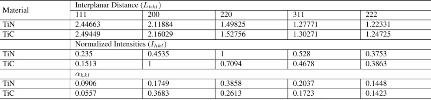
TABLE 1. Data employed for calculation of average titanium atomic distance (DTA) in the interface.
Material Interplanar Distance (Lhkl)
111 200 220 311 222
TiN 2.44663 2.11884 1.49825 1.27771 1.22331
TiC 2.49449 2.16029 1.52756 1.30271 1.24725
Normalized Intensities (Ihkl)
TiN 0.235 0.4535 1 0.528 0.3753
TiC 0.1513 1 0.7094 0.4678 0.3863
αhkl
TiN 0.0906 0.1749 0.3858 0.2037 0.1448
TiC 0.0557 0.3683 0.2613 0.1723 0.1423
All the coatings were produced at 2.5 mbar pressure and 5 mm distance between electrodes. This system has been described in details in previous works [10, 11]. For X-Ray characterization we employed a Bruker AXS diffrac-tometer, model D8 Advance, geometry of parallel beams with graphite monochromator. SEM micrographs were ta-ken with Philips ESEM XL- 30 TPM equipment, allowing for magnifications between 6X and 1200000X, with detector for EDS analysis.
3
Results and Discussion
X- ray diffraction pattern for the Ti/TiN/TiC multilayer is shown in Fig. 1. It was possible to observe peaks (111), (200) and (100) corresponding to FCC structures of TiN and TiC. The fact that both coatings have the same crys-tallographic orientation could be explained by the fact that these two materials, considered as refractory transition me-tal nitride and carbide, have similar characteristics. It should be mentioned that none of these compounds have the ideal rock- salt structure, assumed by theory, but they deviate from the stoichiometry. Moreover, it is found, in the case of these two materials that all three main types of bonding contribute to their refraction properties: metallic contribu-tion with a finite density of states at the Fermi energy,Ef, ionic bonding caused by transfer electrons from the metal to the non-metal atom, and covalent bonds consisting mainly of strong interaction between non-metalpand metald sta-tes, but also on metal/metal interactions [12]. Lattice para-meters in both materials were also measured, with the fol-lowing findings: for TiN 4.23768±0.00125 ˚A and for TiC 4.32058±0.00171 ˚A.
On the basis of the results presented in Table 1, the per-centage of crystallographic planes (hkl) in the TiN and TiC were calculated. See eq. (1).
αT iN hkl =
IT iN
111 IT iN
111 +I
T iN
200 +I
T iN
220 +I
T iN
311 +I
T iN
222
(1)
whereαT iN
111 is the percentage of (111) crystallographic pla-nes in TiN and IT iN
111 the spectral line intensity for (111) crystallographic plane in TiN.
Figure 1. XRD pattern of Ti/TiN/TiC multilayered film.
Considering the lattice parameters and the analysis of the TiN atoms position in the different crystallographic pla-nes of FCC, authors calculated the average titanium atoms distance (LT iN)in TiN and (LT iC)in TiC:
LT iN =α T iN
111 L
T iN
111 +α
T iN
200 L
T iN
200 +α
T iN
220 L
T iN
220
+αT iN311 L
T iN
311 +α
T iN
222 L
T iN
222 (2)
LT iC =α T iC
111L
T iC
111 +α
T iC
200L
T iC
200 +α
T iC
220L
T iC
220
+αT iC311L
T iC
311 +α
T iC
222L
T iC
222 (3) Applying these results the authors have calculated the differences in the average titanium atoms distance (DTA) for layers being in contact with the TiN and TiC interface. LT iN
111 andL
T iC
1750 Brazilian Journal of Physics, vol. 34, no. 4B, December, 2004
(a)
(b)
Figure 2. EDS spectra of the multilayer (a) with electron beam energy of 12 KeV. (b) with electron beam energy of 30 KeV.
The values obtained areLT iN= 1.6076 ˚A andLT iC =
1.7356A˚
DT AT iC−T iN =LT iC−LT iN = 0.128A˚ (4)
whereDT AT iN−T iC is the difference in the average
tita-nium atoms distance for layers being in contact in the inter-face. It is observed that this value is lower than the lattice parameter of TiN and TiC, showing that there is a match in the interlayer. This method is widely explained by J. Smolik et al [13].
Figure 2 shows various EDS spectra taken with different electron beam energy. The spectrum presented in Fig. 2(a) was obtained with 12 keV. Lines of Ti, C, and O were iden-tified, (the last possibly due to the contamination of the film when it is exposed to the environment). The spectrum of Fig. 2(b) was taken at 30 keV of electron beam energy. In this case we observed Ti, C, N, O, and Fe. The elemental composition of the spectra changes with the beam energy because in the first case, the energy is not high enough to al-low the production of characteristic X-ray in the TiN layer. In the second case, the high energy lets the technique get in-formation on all the layers and the substrate. Another way to observe the multilayer composition is to use chemical com-position maps obtained by using EDS. Taking advantage of defects generated when the multilayer was grown, it was
(a)
(b)
(c)
(d)
Figure 3. (a) SEM micrograph using a defect of the multilayer, (b) Chemical map elemental composition for Ti, (c) Chemical map elemental composition for C, (d) Chemical map elemental compo-sition for N. E. Restrepo et. al.
E. Restrepoet al. 1751
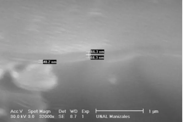
chemical concentration for each layer. Figs. 3(c) and 3(d) represent the chemical map for N and C respectively. The lighter zones in both cases show the concentration of these elements. Fig. 4 shows SEM images of a cross-section of the multilayer, which measured the thickness of each layer. The results are 48 nm for Ti, 66.3 nm for TiN, and 66.3 nm for TiC, observing that these films are very thin.
Figure 4. SEM micrograph employed to measure the thickness of the films.
4
Conclusions
Through XRD, EDS, and SEM a series of Ti/TiN/TiC multi-layers, grown by plasma assisted pulsed-arc discharge, were studied. An agreement was achieved between the chemical composition analysis carried out with different techniques. It was found by using XRD that the TiN and TiC films have the same orientation and crystalline structure, indicating a possible good match between them, due to their similar re-fraction conditions. The elemental chemical maps obtained for the multilayer allowed demonstrating the existence of all the elements that were expected in this case and by using dif-ferent values of electron beam energy, we corroborated that the composition of the film changes as a function of depth.
The thickness of the film was measured by using SEM, obtaining values in the order of nanometers.
Acknowledgments
The author gratefully acknowledge the finantial support of the Division para la Investigaci´on de la Universidad Naci-onal de Manizales (DIMA) and el Instituto Colombiano para el Desarrollo de la Ciencia y la Tecnolog´ıa (Colciencias) du-ring the course of this research, under project RC292-2001
References
[1] L. R. Katipelli, A. Agarwal, and N. B. Dahotre, Mat. Sci. Eng. A289, 34 (2000).
[2] U. Helmersson, S. Todovora, S. A. Barnett, J. S. Sundgren. H. Markett, and J. E. Greene, J. Appl. Phys.62, 481 (1987).
[3] C. J. Tabares, L. Rebouta, B. Almeida, J. Bessa e Sousa, M. F. da Silva, and J. C. Soares, Thin Solid Films317, 124 (1998).
[4] T. S. Li, H. Li, and F. Pan, Surf. Coat. Technol.137, 225 (2001).
[5] J. Smolik, K. Zdunek, Vacuum55, 147 (1999). .
[6] G. Radhakrishnan, P. M. Adams, and D. M. Speckman, Thin Solid Films358, 131 (2000).
[7] J. Wang, W. Z. Li, and H. D. Li, Thin Solid Films382, 190 (2001).
[8] M. H. Shiao, F. S. Shieu, Thin Solid Films386, 27 (2001).
[9] A. Lepone, H. Kelly, and A. Marquez, J. Appl Phys.90, 3174 (2001).
[10] E. Restrepo and A. Devia, J. Vac Sci. technol. A22, 377 (2004).
[11] E. Restrepo, B. Segura, M. Arroyave, and A. Devia, Revista Colombiana de F´ısica,34, 493 (2002).
[12] K. Schwarz and A. Neckel, Phys. Status Solidi B,225, 265 (2001).