This content has been downloaded from IOPscience. Please scroll down to see the full text.
Download details:
IP Address: 79.110.31.51
This content was downloaded on 15/02/2017 at 14:35
Please note that terms and conditions apply.
Inkjet printed metal insulator semiconductor (MIS) diodes for organic and flexible electronic
application
View the table of contents for this issue, or go to the journal homepage for more 2017 Flex. Print. Electron. 2 015003
(http://iopscience.iop.org/2058-8585/2/1/015003)
Home Search Collections Journals About Contact us My IOPscience
You may also be interested in:
Effect of dielectric barrier on rectification, injection and transport properties of printed organic diodes
K E Lilja, H S Majumdar, K Lahtonen et al.
Electrical characterization of the rectifying contact between aluminium and electrodeposited poly(3-methylthiophene)
D M Taylor and H L Gomes
Capacitance–conductance characteristics of Au/Ti/Al2O3/n-GaAs structures with very thin Al2O3 interfacial layer
A Turut, A Karabulut, K Ejderha et al.
Polypyrrole/gold Schottky barrierdiodes
C Nguyen Van, K Potje-Kamloth and C Nguyen Van
Electrical properties of Au/Bi0.5Na0.5TiO3-BaTiO3/n-GaN metal--insulator--semiconductor (MIS) structure
V Rajagopal Reddy, V Janardhanam, Jin-Woo Ju et al.
Printed dielectric-based organic diodes and transistors Kristin Gooden, Amrit Laudari, Grant Knotts et al.
Fabrication and electrical characterization of polyaniline/silicon carbide heterojunctions J F Felix, E A de Vasconcelos, E F da Silva Jr et al.
Flex. Print. Electron 2(2017) 015003 https://doi.org/10.1088/2058-8585/2/1/015003
PAPER
Inkjet printed metal insulator semiconductor (MIS) diodes for
organic and
flexible electronic application
Kalyan Yoti Mitra1,8
, Christoph Sternkiker2 , Carme Martínez-Domingo3,4 , Enrico Sowade1 , Eloi Ramon3,4 , Jordi Carrabina3
, Henrique Leonel Gomes5,6
and Reinhard R Baumann1,7
1 Technische Universität Chemnitz, Digital Printing and Imaging Technology, Chemnitz, Germany 2 Heraeus Noblelight GmbH, Innovation Infrarot, Kleinostheim, Germany
3 Universitat Autónoma de Barcelona, Printed Microelectronics Group, CAIAC(a CSIC Associated Unit), Bellaterra, Spain 4 Institut de Microelectrònica de Barcelona, IMB-CNM(CSIC), Bellaterra, Catalonia, Spain
5 Universidade do Algarve, Campus de Gambelas, Faro, Portugal 6 IT-Instituto de Telecomunicações, Av. Rovisco, Pais, 1, Lisboa, Portugal
7 Fraunhofer Institute for Electronic Nano Systems(ENAS), Department Printed Functionalities, Chemnitz, Germany 8 Author to whom any correspondence should be addressed.
E-mail:[email protected]
Keywords: printed electronics, barrier layers, diodes, inkjet printing
Abstract
All inkjet printed rectifying diodes based on a metal-insulator-semiconductor
(MIS) layer stack are
presented. The rectifying properties were optimized by careful selection of the insulator interlayer
thickness and the layout structure. The different diode architectures based on the following materials
are investigated:
(1) silver/poly (methylmethacrylate-methacrylic acid)/polytriarylamine/silver, (2)
silver/polytriarylamine/poly (methylmethacrylate-methacrylic acid)/silver, and (3) silver/poly
(methylmethacrylate-methacrylic acid)/poly-triarylamine/poly(3,4-ethylenedioxythiophene) poly
(styrenesulfonate). The MIS diodes show an averaged rectification ratio of 200 and reasonable forward
current density reaching 40 mA cm
−2. They are suitable for a number of applications in
flexible
printed organic electronics.
1. Introduction
Inkjet printing is a well accepted deposition technol-ogy for functional materials in the area of printed electronics[1–12]. It allows the precise deposition of
patterned functional layers on both rigid andflexible substrates. Furthermore, inkjet is considered to be an up-scalable deposition technology for industrial appli-cations[13,14]. Inkjet printing enables the
manufac-turing of devices e.g. schottky diodes that are considered as one of the simplest electronic devices in the semiconductor industry [15–19]. They produce
high current density, low forward voltage drops and fast switching behaviour[15–19]. The electrode
mate-rials that can always be considered are e.g. silver(bulk work function: 4.26 to 4.74 eV), copper (bulk work function: 4.53 to 4.98 eV), aluminium (bulk work function: 4.06 to 4.28 eV), poly (3,4 ethylenediox-ythiophene) poly (styrenesulfonate) (PEDOT:PSS, bulk work function: 5.1 eV) [20, 21]. Either one of
these functional conductive materials look simple to
process, but in most of the cases it is challenging to appoint and locate them (having different work functions) adjacent to the semiconductor interface layer [22]. Recently, it has been reported that MIS
structures show a rectifying behaviour[23–26]. In the
inorganic MIS devices where the conventional insulat-ing silicon dioxide(SiO2) thickness is below 7 nm, the
charge carriers can tunnel through the insulating barrier[27,28]. This causes a reduction in the reverse
saturation current and an increase in the barrier height in the energy band diagram[27,28]. On the contrary, a
thick insulating layer with 50 to 200 nm will block the charge carrierflow and will not show rectification [26].
However, if the insulator layer is leaky due to an irregular morphology produced by the mutual action/blend of the semiconductor to insulator inter-faces it can lead to a voltage controlled leakage and to corresponding asymmetric current versus voltage curves[22]. Herein, we focus on assessing the electrical
characteristics of MIS based diodes fabricated comple-tely by inkjet printing technology. The complete layer
RECEIVED
27 May 2016
REVISED
7 November 2016
ACCEPTED FOR PUBLICATION
15 November 2016
PUBLISHED
10 February 2017
stack consists of:(a) top and bottom printed conduc-tive layers using a silver nano-particle ink and in other case PEDOT:PSS,(b) a polymeric insulator layer using poly(methylmethacrylate-methacrylic acid in ethtyl lactate) MMAcoMAA and (c) a polymeric polytriar-ylamine PTAA semiconducting layer. Due to the interaction between the MMAcoMAA and the semi-conductor a MIS diode is obtained showing a rectify-ing behaviour [22]. Moreover, the yield of the MIS
diode devices will be studied to ensure a reliable technology.
2. Experimental
2.1. Fabrication and characterization
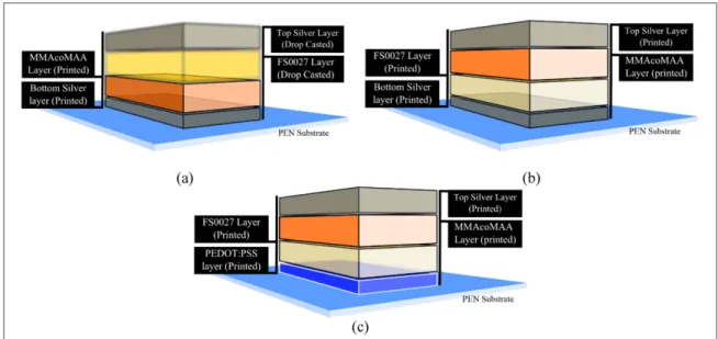
Three types of MIS diode architectures are reported here. The schemes for the MIS diode architectures are shown infigure1. Inkjet printing of MIS diodes was conducted based on the architecture mentioned in figure1. Silver nanoparticle ink from SunTronic EMD 5603(SunChemical), PEDOT:PSS ORGACON™ IJ-1005 (Agfa-Gevaert N.V.), MMAcoMAA from (MicroChem Corp.) and PTAA p-type organic semi-conductor(FS0027, from Flexink Ltd) were used as the functional inks for manufacturing these MIS diodes on a heat stabilized 125μm thick polyethylene naphthalate (PEN) Teonex Q65FA substrate from Dupont Teijin Films.
The inkjet printing of the functional layers was performed using the Dimatix Material Printer DMP-2831 from Fujifilm Dimatix Inc. using standard devel-opment printheads(DMC) with 10 pL nominal drop volume. For Architecture no. 1, printing was per-formed solely for bottom silver and MMAcoMAA lay-ers. For Architecture no. 2 and Architecture no. 3, the entire layer stacks were inkjet printed. Table1shows an overview of the printing methodology, printing parameters as well as curing/sintering parameters for
the individual functional layer used for manufacturing the MIS diodes. The aim to use PEDOT:PSS as an anode was to achieve an semi-organic diode by means of replacing the bottom silver electrode.
For all of the three MIS diode architectures, the thickness of the MMAcoMAA layer was varied incre-mentally to study the effect of the rectification. This was done by changing the number of layers, but keep-ing the drop space constant. The active area for the MIS diodes(for Architecture no. 2 and Architecture no.(3) was kept constant. After fabricating the MIS diodes, the layers were optically characterised with light microscopy Leica DM 4000 M and by scanning electron microscopy (SEM) processed with focused ion beam (FIB) cut. Subsequently, the MIS diodes were electrically characterized using a Keithley 2636A source meter connected to a Suess mess probe station. Positive voltages(forward bias) refers to the top silver electrode for all the architectures. All electrical mea-surements were performed under ambient conditions.
3. Results
3.1. Optical analysis
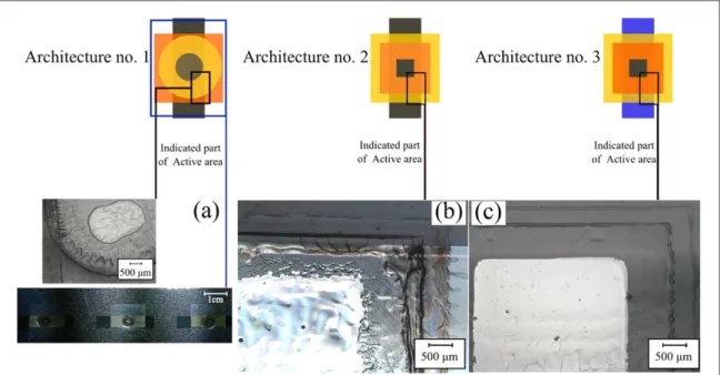
Figure2depicts the microscopic images and photo-graphs for the three MIS diode architectures. Through the microscopic image and also the photograph, the MIS diode from Architecture no. 1 shows a top silver layer which has been drop casted and which has no definite form. Due to the stacked position of the layer in this architecture, it was seen that the drop casted top silver electrode exhibited contraction in its dimension. Also, it was detected that the shape for the drop casted top silver is irregular due to the process of the deposition itself and the low surface energy possessed by the FS0027 organic semiconductor layer.
In contrast to this, Architecture no. 2 is an all-inkjet printed MIS diode. A microscopic image for the
Figure 1. Schematic diagrams for the different MIS diodes(a) Architecture no. 1, (b) Architecture no. 2, and (c) Architecture no. 3.
Table 1. Overview of printing and curing/sintering parameters.
Layer Sequence 1st 2nd 3rd 4th
Architecture no. 1 Deposition process Inkjet Printing Technology Inkjet Printing Technology Drop Casted Drop Casted Partially inkjet printed MIS
diodes
Layer Bottom electrode (silver) Barrier layer (MMAcoMMA) Organic semiconductor (FS0027) Top electrode(silver)
Number of layers 1 1, 3, 6, 12 1 1
Drop space(μm) 20 20 — —
Pattern size(mm × mm) 7×5 5×5 — Approximately 25
Post-treatment in hot plate (min, °C)
20, 120 60, 150 20, 100 20, 120
Architecture no. 2 Deposition process Inkjet Printing Technology Inkjet Printing Technology Inkjet Printing Technology Inkjet Printing Technology All inkjet printed MIS diodes
Layer Bottom electrode(silver) Organic semiconductor(FS0027) Barrier layer(MMAcoMMA) Top electrode(silver)
Number of layers 1 2 1, 3, 6, 12 2
Drop space(μm) 20 20 20 20
Pattern size(mm × mm) 7×5 5×5 4×4 3×3
Post-treatment in oven(min, °C) 30, 135 20, 100 60, 150 30, 135
Architecture no. 3 Deposition process Inkjet Printing Technology Inkjet Printing Technology Inkjet Printing Technology Inkjet Printing Technology All inkjet printed MIS diodes
Layer Bottom electrode
(PEDOT:PSS)
Organic semiconductor(FS0027) Barrier layer(MMAcoMMA) Top electrode(silver)
Number of layers 1 2 1, 3, 6, 12 2
Drop space(μm) 10 20 20 20
Pattern size(mm × mm) 7×3 4×4 5×5 3×3
Post-treatment in oven(min, °C) 6, 120 20, 100 60, 150 30, 135
3 Flex. Print. Electron 2( 2017 ) 015003 K Y Mitra et al
fabricated diode can be seen infigure2(b) at the corner
involving 3 layers(as an example) of MMAcoMAA. The other layers which constitute the MIS diode can be also seen, such as the bottom silver electrode, FS0027 organic semiconductor and the top silver elec-trode. The basic difference in this architecture can be found in the position of the MMAcoMAA and the FS0027 organic semiconductor layer. They are inter-changed, so as to facilitate improved wetting of the sil-ver ink and therefore the printing process to complete the diode layer stacks. Although it was seen that the layer formations (MMAcoMAA) for the fabricated diode are not very uniform. This characteristic beha-viour of the layer arrives from the subsequent drying procedure of the ink during the printing process. This characteristic inhomogeneity is then transferred to the next succeeding layer until it reaches the top silver electrode. Occasionally, de-wetting of the silver ink (for the top electrode) was observed which refers to the high quantitative involvement of the MMAcoMAA layer with FS0027 organic semiconductor with respect to the printed area. For thefinal Architecture no. 3, a microscopic image can be seen for the MIS diode, again involving 3 layers MMAcoMAA. Due to the high smoothness of the PEDOT:PSS layer, the next stacked succeeding layers were expected to show similar and improved layer formation. This behaviour can be directly seen in the depicted microscopic images. The silver electrode is also found to exhibit better wetting and contribute to good layer formation. Although occasionally again, the layer formation was seen to be disturbed, but this is due to the high quantitative involvement of the MMAcoMAA material. In addition to this, SEM images were also taken for the analysis of the layer internally through the cross section of the printed layers which is made by a FIB cut. The FIB cut was made across the printing direction for the
fabricated MIS diodes. Figure3gives an overview of the inkjet printed layers. Figure3(a) shows the layer
stack of the PEDOT:PSS and FS0027 organic semi-conductor(from bottom to top) and figure3(b) silver
and MMAcoMAA layers(from bottom to top). As the analysis of the layer quality and thickness reveals, the printed layers were seen to bind together without any definite interfaces which can be caused dur-ing the printdur-ing process. But infigure3(b) some air
bub-ble like structures were detected which can be the cause of the deposited ink and the subsequent drying of the layer itself. We believe that during the jetting process some air bubbles are generated and these bubbles get trapped once the drying phenomenon already starts internally during the printing phase. For the analysis, sin-gle printed layers for each individual material were con-sidered but with different drop spaces(optimal value necessary to obtain a continuous and smooth layer). The used drop space for the printing of these PEDOT:PSS, silver, MMAcoMAA and FS0027 layers were 10μm, 20μm, 20 μm and 20 μm respectively. The average thicknesses from the individual PEDOT:PSS, silver, MMAcoMAA and FS0027 layers were found to be 0.6±0.01 μm, 0.3±0.01 μm, 1.7±0.02 μm, and 0.7±0.03 μm respectively. The thickest value can clearly be detected from the printed MMAcoMAA layer. It can also be concluded that the total thickness of the MIS diodes in Architecture no. 2 and Architecture no. 3 will vary according to the number of MMAcoMAA layers which is printed furthermore.
3.2. Electrical analysis
The analysis of the electrical characteristics for the printed MIS diodes for the different architectures was performed on the basis of current density versus voltage(J–V ) curves. The measurements are based on
Figure 2. Microscopic images and photos of the MIS diodes for(a) Architecture no. 1, (b) Architecture no. 2, and (c) Architecture no. 3.
the obtained current modulations when the different voltage values are biased on the fabricated MIS diodes (step of 1.0 V, applied from +10.0 V to −10.0 V). Every time, 20 MIS diode samples are considered from each diode architecture. The optimal results based on the tendency of the diodes(out of 20 samples) and with respect to the three architectures are considered here. On the basis of these results, a rectification ratio is also calculated. The rectification ratio here can be defined as the proportion(ratio) of the obtained current at the biased positive to the negative of the same voltage (modulus). The values for the quantity and stability of the rectification ratio will define the quality of the diode and its short term reliability. In addition to this, cumulatively the fabrication yield and performance of the MIS diodes are derived for the all inkjet printed diode architectures.
3.2.1. Architecture no. 1
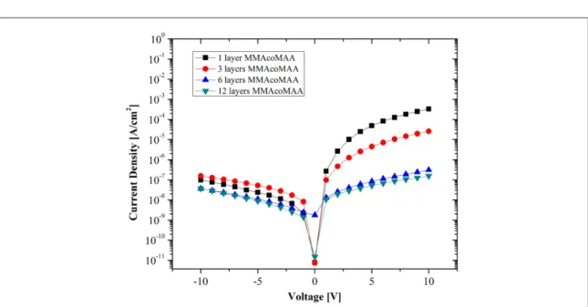
Figure 4 shows the J–V curve for the MIS diodes
comprising of Architecture no. 1. The different characteristics correspond to the use of several
interlayer thickness constituting 1 layer, 3 layers, 6 layers, and 12 layers of MMAcoMAA respectively. For the diodes having 1 layer of MMAcoMAA, the maximum(max) forward current density (current at positive voltage for the defined active area) is seen to reach 300μA cm−2at +10.0 V, whereas at −10.0 V the reverse current density(current at negative voltage for the defined active area) can be seen to reach 0.1μA cm−2. This low value exhibited here is prefer-able for low leakage current and better diode perfor-mance. Persistently, the working of the diode is exhibited with the quantity of current in several tens towards hundreds ofμA cm−2.
For the diodes with 3 layers of MMAcoMAA, the highest forward current density is 20μA cm−2 at +10.0 V, and 0.15 μA cm−2 in reverse current at
−10.0 V. The working of the diode is exhibited at the forward voltage regime with the quantity of current density tending towards fewμA cm−2. Similarly, the diodes having 6 layers of MMAcoMAA, the max obtained forward current density is 0.3μA cm−2 at +10.0 V, and 40 nA cm−2in reverse current density at
Figure 3. SEM images of the cross-section containing(a) PEDOT:PSS and FS0027 (bottom to top), and (b) silver and MMAcoMAA (bottom to top).
Figure 4. Graph showing a characteristic J–V curve for MIS diodes as function of MMAcoMAA layers (Architecture no. 1).
5
−10.0 V. In this case, the difference in the quantity of the obtained current at the forward and reverse direc-tion was found to be minimum(min), although the reverse current or the leakage current is found to be similar. For the diodes with 12 layers of MMAcoMAA, the max obtained forward current density is 0.16μA cm−2at+10.0 V, and 40 nA cm−2in reverse current density at−10.0 V. The values of current at both the forward and reverse regime are found to be low in quantities. A definite dip in the values for the forward current is seen when the diodes are compared with respect to the increasing number of MMAco-MAA layers. The shape of the curves depicted here can also be seen toflatten out on both the voltage regimes for the diodes containing 6 and 12 layers of MMAco-MAA. The best diode characteristic is obtained from 1 layer and 3 layers of MMAcoMAA.
3.2.2. Architecture no. 2
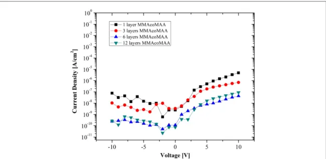
Infigure5, a J–V curve is shown for the MIS diodes
comprising of Architecture no. 2. For the diodes with 1 layer of MMAcoMAA, the max obtained forward current density is 6μA cm−2 at +10.0 V, and 70 nA cm−2 in reverse current density at −10.0 V. Again this obtained low and high value of the current densities at the reverse and forward regime for the applied voltage result in good rectification. For the diodes with 3 layers of MMAcoMAA, the max obtained forward current density is 0.7μA cm−2 at +10.0 V, and 10 nA cm−2in reverse current density at
−10.0 V. On the contrary, for the diodes with 6 layers of MMAcoMAA, the max obtained forward current density is 40 nA cm−2at+10.0 V, and 0.2 nA cm−2in reverse current density at−10.0 V.
Similar characteristic results were obtained for the diodes with 12 layers of MMAcoMAA, with 90 nA cm−2and 0.3 nA cm−2current densities in the forward and reverse voltage regime. A dip in the values
for the forward current density is seen when the diodes are compared with respect to the increasing number of MMAcoMAA layers. In both cases, for the diodes with 6 and 12 layers of MMAcoMAA, the quantity of the max reverse current density detected is extremely low, but so is the max forward current. The shape of the J– V curve is more ideal for the condition where the diode contains 1 layer and 3 layers of MMAcoMAA. The shape of the curves depicted here do notflatten out at all. The best diode characteristic is obtained again from 1 layer and 3 layers of MMAcoMAA.
3.2.3. Architecture no. 3
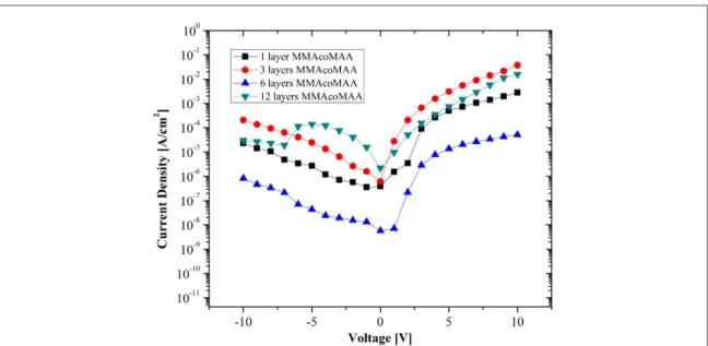
Infigure6, a J–V curve is shown for the MIS diodes
comprising of Architecture no. 3. For the diodes with 1 layer of MMAcoMAA, the max obtained forward current density is 3 mA cm−2 at +10.0 V, and 20μA cm−2in reverse current at−10.0 V. The diodes having 3 layers of MMAcoMAA, the max obtained forward current is 40 mA cm−2 at +10.0 V, and 0.2 mA cm−2 in reverse bias at −10.0 V. On the contrary, for the diodes with 6 layers of MMAcoMAA, the max obtained forward current is 50μA cm−2at+ 10.0 V, and 0.8μA cm−2 in reverse current at −10.0 V. Similarly, for the diodes with 12 layers of MMAcoMAA, the max obtained forward current reaches 20 mA cm−2at+10.0 V, and 30 μA cm−2in reverse current at−10.0 V. There is a dip in the values for the forward current when the diodes are compared with respect to the increasing number of MMAcoMAA layers. In all the cases for this diode architecture, the quantity of the max reverse saturation current detected is high(in μA) and so is the max forward current (in mA). The curves do not flatten out on both the forward and reverse voltage regimes. The best diode is obtained from 1 layer and 3 layers of MMAcoMAA(considering best stability and highest forward current density).
Figure 5. Graph showing a characteristic J–V curve for MIS diodes as function of MMAcoMAA layers (Architecture no. 2).
The function of the varying MIS diode archi-tectures against the thickness of the MMAcoMAA bar-rier layer for the swept voltage range is analysed. the rectification ratio versus biased voltages can be observed in three parts for 1 layer, 3 layers, 6 layers and 12 layers of MMAcoMAA. Thefirst, second and third part gives an overview for Architecture no. 1, Archi-tecture no. 2 and ArchiArchi-tecture no. 3, respectively.
It was found that for Architecture no. 1, max and min values for the rectification ratios considering that 1 layer of MMAcoMAA involved in the diode layer stack were between 3311.5 (3312 approx.) to 121.6 (122 approx.), respectively), with a difference of 3190 approx.; considering 3 layers of MMAcoMAA between 164.4(164 approx.) to 12.1 (12 approx.) with a differ-ence of 152 approx.; considering 6 layers of MMAco-MAA between 314 to 2.6(12 approx.) with a difference of 311 approx.; and considering 12 layers of MMAco-MAA between 2320.3(2320 approx.) to 4.2 (4 approx.) with a difference of 2316 approx. When all the values corresponding to this architecture are analysed at the end, it could be concluded that for Architecture no. 1 and including 1 layer and 3 layers a trend toward the increasing rectification ratio is given. But similarly, for the same architecture and the diodes containing 6 and 12 layers of MMAcoMAA, disturbances at the begin-ning of the voltage biasing are evident. These dis-turbances could be explained by the behaviour of the low reverse and relatively high forward current at low voltage(around 2 V to 3 V). The best resulting diode can be obtained from the stack where the number of MMAcoMAA layers is 1.
As for Architecture no. 2, max and min values for the rectification ratios considering that 1 layer of MMAcoMAA involved was between 107 approx. to 2 approx., respectively, with a difference of 105 approx.; considering 3 layers of MMAcoMAA between 116.7 (117 approx.) to 1.7 (2 approx.) with a difference of
115 approx.; considering 6 layers of MMAcoMAA between 175.3(175 approx.) to 8.5 (9 approx.) with a difference of 167 approx.; and considering 12 layers of MMAcoMAA between 536.4(536 approx.) to 5.1 (5 approx.) with a difference of 531 approx. When all the values corresponding to the different number of MMAcoMAA layers are considered among themselves for a particular diode architecture, then an increasing trend can be seen with a minimum amount of differ-ence. Since the values for the rectification ratios obtained among the same kind of diodes themselves are very close to each other, therefore they are stable. The best resulting diodes can be obtained from the stack where the number of MMAcoMAA layers is 1 and 3.
For the last Architecture no. 3, max and min values for the rectification ratios considering that 1 layer of MMAcoMAA involved was between 219.7 (220 approx.) to 4.2 (4 approx.) respectively, with a differ-ence of 216 approx.; considering 3 layers of MMAco-MAA between 182.1(182 approx.) to 17.4 (17 approx.) with a difference of 165 approx.; considering 6 layers of MMAcoMAA between 321.4(322 approx.) to 0.5 (1 approx.) with a difference of 321 approx; and con-sidering 12 layers of MMAcoMAA between 528.4(529 approx.) to 0.6 (1 approx.) with a difference of 528 approx. When all the values corresponding to the dif-ferent number of MMAcoMAA layers are considered among themselves for this diode architecture, then an increasing trend can be seen with a large amount of disturbances. The best resulting diode can be obtained from the stack where the number of MMAcoMAA lay-ers is 3.When all the curves are considered with regards to all the mentioned architectures and also the number of MMAcoMAA layers then it can be said that the best diode can be fabricated using 1 or 3 layers of MMAcoMAA in function of the voltage applied to the device.
Figure 6. Graph showing a characteristic J–V curve for MIS diodes as function of MMAcoMAA layers (Architecture no. 3).
7
For the second condition, the rectification ratios concerning the average value and their standard devia-tion are considered. In this secdevia-tion, the quantity of deviation is also considered which will indicate the sta-bility of the diodes. The average values for the rectifica-tion ratio of the diodes for Architecture no. 1 for the different MMAcoMAA layers involved are as follows: 1 layer: 1820±1299, 3 layers: 84±58, 6 layers: 35±93 and 12 layers: 252±696 respectively. Simi-larly, the average rectification ratio for the diodes belonging to Architecture no. 2 containing a different number of MMAcoMAA layers are as follows: 1 layer: 42±37, 3 layers: 54±45, 6 layers: 60±50 and 12 layers: 111±169 respectively. And, for the diodes belonging to Architecture no. 3 containing a different number of MMAcoMAA layers are as follows: 1 layer: 124±86, 3 layers: 111±58, 6 layers: 133±122 and 12 layers: 125±192 respectively. As a conclusion for the results, for all the architectures and 12 layers of MMAcoMAA involved, the amount of the standard deviation observed is the highest. Therefore, these diodes cannot be totally reliable. The reasons can be predicted from the high amounts of MMAcoMAA material deposited and thereby its strong interaction with the semiconductor layer. For Architecture no. 1, the best result for the diodes can be seen when the number of MMAcoMAA layers is 1. Even though the diodes exhibit the highest standard deviation, it also shows the highest rectification ratio (average value). The reason for this high deviation can be due to low performance at low voltages. For the diodes which are all inkjet printed belonging to Architecture no. 2, the best results can be seen when the number of MMAco-MAA layers is 3. The diodes show the maximum recti-fication ratio (average value) and comparatively the lowest standard deviation. Again for the diodes which are all inkjet printed belonging to Architecture no. 3, the best result for the diodes can be seen when the number of MMAcoMAA layer is 1. The diodes show
relatively good rectification ratio (average value) and also low standard deviation.
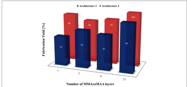
It is believed that the physics behind the function-ality of the MIS diode lies inside the stack of materials itself. It is known that when there is a deposition of one layer over the another layer(especially in a solu-tion processing technique e.g. inkjet printing of the individual layers), the solvents and the polymer con-tents in the liquid state might interact with the cured layer beneath. The most interesting interaction is the FS0027 semiconductor to MMAcoMAA insulator interface. In this condition, it can be also expected that several networks might form and they might also contain polymers from counter interface layers e.g. formation of micro to nanoscale FS0027 networks in MMAcoMAA. It is already experienced that MMA-coMAA(being a polymer material with leaky proper-ties) presents a high current through the structure for the forward bias. This explains that with increasing the thickness of the dielectric layer the current decreases, thereby blocking the current. Under reverse bias, the interface of MMAcoMAA and FS0027 is depleted. It is speculated that the junction of the dielectric layer and silver electrode blocks the current, due to the addition of an extra energy barrier in comparison to FS0027, which presents an ohmic contact in the presence of the silver electrode. Because the semiconductor FS0027 is deposited before the MMAcoMAA a network is produced and rectification behaviour is obtained. This demon-strates that apart from the use of a leaky dielectric, it is necessary to create a network among the dielectric semiconductor regardless of the work function of the bottom electrode, i.e. silver or organic polymer. In figure7, the graphs containing the fabrication yield of the diode samples belonging to Architecture no. 2 and Architecture no. 3(all inkjet printed MIS diodes) are shown. The focus is based on the architectures and the number of MMAcoMAA layers involved. The
Figure 7. Graph showing the fabrication yield of MIS diodes containing Architecture no. 2, and Architecture no. 3.
calculation for the fabrication yield is made accord-ing to two classes:(1) working devices (similar work-ing), and (2) non working or short-circuit or no rectifying diodes. As mentioned earlier, every time 20 samples are considered for Architecture no. 1, the calculated fabrication yield was found to be between 50 to 60% for all the different numbers of MMAco-MAA layers. But, for Architecture no. 2, the fabrica-tion yield was found to be different. The highest fabrication yields of 90% and 70% were achieved for the diodes involving 12 layers and 3 layers of MMA-coMAA. In general, when 1 layer, 3 layers, 6 layers and 12 layers of MMAcoMAA are considered, then the average yield can found to be 70±15%. When only 1 layer, 3 layers and 6 layers of MMAcoMAA are considered then the average yield is found to be 63±8%. The best compromise can be seen for the diodes with 3 layers of MMAcoMAA. But, for Archi-tecture no. 3, the fabrication yield was found to be different. The highest fabrication yields of 100% and 90% were achieved for the diodes involving 12 layers and 1 layer of MMAcoMAA. In general, when 1 layer, 3 layers, 6 layers and 12 layers of MMAcoMAA are considered, then the average fabrication yield can found to be 89±9%. When only 1 layer, 3 layers and 6 layers of MMAcoMAA are considered then the average yield is found to be 85±5%. The best com-promise is observed for the diodes with 3 layers of MMAcoMAA. It could be predicted that this high fabrication yield for Architecture no. 3 MIS diodes is because of the involvement of the PEDOT:PSS as an electrode. The material gives a suitably low surface roughness (Ag∼20 nm, PEDOT:PSS∼5 nm) for the development of diodes. Of course, the involve-ment of more numbers MMAcoMAA layers for both architectures gives the highest fabrication yield for e.g. 12 layers, resulting to diodes which give rise to a low number of electrical short-circuits, but they are more prone to the high quantity of disturbance in terms of the electrical characteristics.
4. Conclusion
In summary, the electrical properties of rectifying diodes based on a MIS structure were optimized by the proper selection of device architecture and insulator layer thickness. It can be concluded that for MIS diode Architecture no. 1, Architecture no. 2 and Architecture no. 3, the best rectifying diode properties can be achieved when the entire stack includes 1 layer, 3 layers and 1 layer of MMAcoMAA respectively. The decision is made taking into account several diode parameters, namely, the diode property like current density versus voltage characteristic curves, current density, rectifica-tion ratios, standard deviarectifica-tions and fabricarectifica-tion yield. From the results, it can be concluded that above a certain dielectric thickness the rectifying properties degrade and the diode becomes resistive between the
electrodes and thus the electrical performance decreases. Therefore, the amount of MMAcoMAA layers and the interaction of the FS0027 onto the MMAcoMAA is crucial to obtain a good rectifying behaviour effect. The fabrication yield for achieving good diodes is increased using a smoother layer such as PEDOT:PSS since the work function of both electrodes is not responsible for the rectifying behaviour. It can be reported that these MIS diodes are a new unconven-tional route for fabricating rectifying diodes. The diodes can be fabricated for various applications with the possibility of using either identical or dissimilar materi-als for the two electrodes. These types of diodes are all inkjet printed with a fabrication yield of approx. 70 to 80% at atmospheric conditions.
Acknowledgments
This research work was supported by the EU funded project: Technology & Design Kits for Printed Electro-nics (TDK4PE), grant agreement no.: 287682. The authors for this research work thank TDK4PE for the inspiration, team work, and research performed related to the exploration of functional materials leading to developing new device fabrication routes and the process of inkjet printing. We would also like to thank Mr Dirk Rittrich(Department of Layer Deposition at Fraunhofer ENAS) for his support with SEM analysis.
References
[1] Chung S et al 2011 All-inkjet-printed organic thin-film transistors with silver gate, source/drain electrodes Japan. J. Appl. Phys.50 03CB05(1–5)
[2] Kawase T et al 2005 Inkjet printing of polymeric field-effect transistors and its applications Japan. J. Appl. Phys.44 3649–58
[3] Chung S et al 2011 All-inkjet-printed organic thin-film transistor inverter onflexible plastic substrate IEEE Electron Device Lett.32 1134–6
[4] Castro H F et al 2014 All-inkjet-printed bottom-gate thin-film transistors using UV curable dielectric for well-defined source-drain electrodes J. Electron. Mater.43 2631–6
[5] Castro H F et al 2015 Degradation of all-inkjet-printed organic thin-film transistors with TIPS-pentacene under processes applied in textile manufacturing J. Org. Electron.12–9 [6] Mitra K Y et al 2015 Potential up-scaling of inkjet-printed
devices for logical circuits inflexible electronics AIP Conf. Proc. 1646 106–14
[7] Jang J et al 2013 High performance ink-jet printed diketopyrrolopyrrolebased copolymer thin-film transistors using a solution processed aluminium oxide dielectric on a flexible Substrate J. Mater. Chem. C1 2408–11
[8] Hong J-P et al 2008 Tuning of Ag work functions by self-assembled monolayers of aromatic thiols for an efficient hole injection for solution processed triisopropylsilylethynyl pentacene organic thinfilm transistors Appl. Phys. Lett.92 (1-3)143311
[9] Liu Y et al 2012 An all-inkjet printed flexible capacitor on a textile using a new poly(4-vinylphenol) dielectric ink for wearable applications Proc. in Sensors IEEEpp 1–4 [10] Liu Y et al 2012 An all-inkjet printed flexible capacitor for
wearable applications Symp. on Design, Test, Integration and Packaging of MEMS/MOEMS (Cannes Côte d’Azur, France) pp 192–5
9
[11] Kang B J et al 2012 All-inkjet-printed electrical components and circuit fabrication on a plastic substrate Microelectron. Eng. 97 251–4
[12] Cook B S et al 2013 Multi-layer RF capacitors on flexible substrates utilizing inkjet printed dielectric polymers Microw. Wireless Compon. Lett.23 353–5
[13] Fukuda K et al 2014 Fully solution-processed flexible organic thinfilm transistor arrays with high mobility and exceptional uniformity Sci. Rep.4 1–8
[14] Abbel R et al 2014 Industrial-scale inkjet printed electronics manufacturing—production up-scaling from concept tools to a roll-to-roll pilot line Trans. Mater. Res.1 1–13
[15] Marjanovic N et al 2011 Inkjet printing and low temperature sintering of CuO and CdS as functional electronic layers and Schottky diodes J. Mater. Chem.21 13634–9
[16] Steudel S et al 2008 Ultra-High frequency rectification using organic diodes Proc. in Electron Devices Meeting (San Francisco, USA)pp 1–4
[17] Lin C-Y et al 2011 High-frequency polymer diode rectifiers for flexible wireless power-transmission sheets J. Org. Electron.12 1777–82
[18] Heljo P S et al 2013 Printed half-wave and full-wave rectifier circuits based on organic diodes Transl. Electron Devices60 870–4
[19] Park H et al 2012 Fully roll-to-roll gravure printed rectenna on plastic foils for wireless power transmission at 13.56 MHz Nanotechnology23 1–6
[20] Michaelson H B 1977 The work function of the elements and its periodicity J. Appl. Phys.48 4729–33
[21] Nardes A M 2008 Conductivity, work function, and environmental stability of PEDOT:PSS thinfilms treated with sorbitol J. Org. Electron.9 727–34
[22] Mitra K Y et al 2013 Inkjet-printed rectifying metal-insulator-semiconductor(MIS) diodes for flexible electronic
applications MRS Proc. Fall 2013 (Boston, USA)pp 1–7 [23] LiljaKE etal 2011Enhanced performance ofprinted organic diodes
using a thin interfacial barrier layer Appl. Mater. Interfaces3 7–10 [24] Jung M et al 2010 All-printed and roll-to-roll-printable
13.56 MHz-operated 1-bit RF tag on plastic foils Transl. Electron Devices57 571–80
[25] Steudel S et al 2006 Comparison of organic diode structures regarding high-frequency rectification behaviour in radio-frequency identification tags J. Appl. Phys.99 1–7
[26] Lilja K E et al 2009 Gravure printed organic rectifying diodes operating at high frequencies J. Org. Electron.10 1011–4 [27] Sze S M and Ng K K 2007 Physics of Semiconductor Devices 3rd
edn(New York: John Wiley & Sons) pp 417–37
[28] Hudait M K and Krupanidhi S B 2000 Solid-State Electron.44 1089–97