ACÁCIO JOÃO GALHARDO BAPTISTA
NOVEL TECHNIQUES FOR THE DESIGN AND
PRACTICAL REALIZATION OF
SWITCHED-CAPACITOR CIRCUITS IN DEEP-SUBMICRON
CMOS TECHNOLOGIES
Dissertação apresentada para obtenção do Grau de Doutor em Engenharia Electrotécnica e de Computadores pela Universidade Nova de Lisboa, Faculdade de Ciências e Tecnologia
Acknowledgements
I owe thanks to many people for the successful realization of this Thesis.
I am deeply grateful to Prof. João Goes for his support, commitment, advising and supervising, for the optimism, motivation and encouragement I received along this period.
I thank to all colleagues and friends for the technical support and share, namely to Bruno Esperança and Ricardo Gama.
I would like also to mention and thank to João Neto and Miguel Santos (from ACACIA, now S3), respectively for the precious help on the realization of the integrated prototype of the complete ADC, and for the experimental evaluation of it.
Sumário
Interruptores exibindo elevada linearidade são cada vez mais essenciais em circuitos de condensadores comutados, nomeadamente em conversores analógico-digital de resoluções entre os 12 e os 16 bits. A tecnologia CMOS evolui continuamente em direcção a tensões de alimentação cada vez mais reduzidas, e simultaneamente, novas técnicas de projecto são necessárias para possibilitarem a realização de interruptores que exibam uma elevada gama dinâmica e uma distorção compatível com as resoluções referidas. Para além disso, com a diminuição contínua das dimensões, as restrições físicas da tecnologia deverão ser tidas em linha de conta, de modo a evitar o stress excessivo dos dispositivos quando relativamente elevadas tensões são aplicadas às suas portas. Novas técnicas de linearização de interruptores com fiabilidade elevada terão necessariamente que ser investigadas e demonstradas em circuito integrado CMOS.
Também é constante a procura de novas estruturas de circuitos com condensadores comutados. São indispensáveis estruturas simplificadas e eficazes, adequadas às novas exigências decorrentes da proliferação do uso de equipamentos portáteis, necessariamente com baixo consumo de energia, mas assegurando alto desempenho de múltiplas funções.
Abstract
Switches presenting high linearity are more and more required in switched-capacitor circuits, namely in 12 to 16 bits resolution analog-to-digital converters. The CMOS technology evolves continuously towards lower supply voltages and, simultaneously, new design techniques are necessary to fulfill the realization of switches exhibiting a high dynamic range and a distortion compatible with referred resolutions. Moreover, with the continuously downing of the sizes, the physic constraints of the technology must be considered to avoid the excessive stress of the devices when relatively high voltages are applied to the gates. New switch-linearization techniques, with high reliability, must be necessarily developed and demonstrated in CMOS integrated circuits.
Also, the research of new structures of circuits with switched-capacitor is permanent. Simplified and efficient structures are mandatory, adequate to the new demands emerging from the proliferation of portable equipments, necessarily with low energy consumption while assuring high performance and multiple functions.
Symbols and Abbreviations
A Amplifier open-loop gain
AD Drain area
Ain Input voltage amplitude peak-to-peak
AS Source area
AVT Threshold voltage matching parameter
B Stage effective resolution
b0, b1 Quantizer output codes
C Capacitor
Ca Charge pump capacitor
Cb Bootstrap capacitor
CBC Bulk-channel capacitance
CC Compensation capacitor
CF Feedback capacitor
Cg Gate capacitance
CGC Gate-channel capacitance
CGD Gate-drain capacitance
CGD0 Gate-drain overlapped capacitance
CGG Gate-gate capacitance
CGS Gate-source capacitance
CGS0 Gate-source overlapped capacitance
Cij Two-terminal, i and j, capacitance
CjBC Bulk-channel junction capacitance per unit area
CjDB Drain-bulk junction capacitance per unit area
CjSB Source-bulk junction capacitance per unit area
CL Load capacitance
clk Master clock
Cox Oxide capacitance per unit area
CP Parasitic capacitor
cr Ratio of divided channel charge
CS Sampling capacitor
CS(S/H) S/H sampling capacitor
Cu Unity capacitance
Di Multiplier of reference voltage
EOT Eqivalent oxide thickness
Eox Oxide field
fgate Gate corner frequency
fin Input frequency
FS Sampling frequency
F Clock frequency
g Conductance
G Gain
GC(T) TDDB temperature dependent parameter
gDS Drain-source conductance
gEQ Equivalent conductance
gm Transconductance
gtunnel Tunnel conductance
h Strong-to-weak inversion variation
i Current
I Current source
IDD Supply current
iDS Drain-source current
Ig Gate leakage current
iGS Gate-source current
Ij Gate induced drain leakage current
Imax Maximum current
Ioff OFF-state leakage current
iout Output current
k Boltzmann constant and scaling factor
K1, K2 Capacitor ratio factors
KP Mobility factor
L Channel length
LD Overlapped length
nS Number of cascade stages
p PMOS or positive suffix
P Power
PD Power dissipation
PU Useful power
q Unity charge
q0, q1, q2 Comparator outputs codes
QC Channel or capacitor charge
QCP Parasitic capacitance charge
QCS Sampling capacitor charge
Qi Terminal i charge
Qv Charge per voltage
RD Degeneration resistor
RDS Drain-to-source resistance
RF Feedback resistor
RL Load resistor
ro Device output resistance
Ro Amplifier output resistance
Rout Stage output resistance
RS Voltage multiplier series resistance
SR Slew-rate
sT Sub-threshold slope factor
t Time
T Temperature
TDDB Time dependent dielectric breakdown
tox Oxide thickness
toxeff Effective oxide thickness
tSR Slew-rate time
VB Biasing voltages
vBS Bulk-to-source voltage
VCM Common mode voltage
VCMI Input common mode level
VCMO Output common mode level
VDD Positive supply voltage
vDS Drain-to-source voltage
VDSsat Drain-to-source saturation voltage
VEn Early voltage per channel length
VHI Common mode level, high
vG Gate voltage
vGD Gate-to-drain voltage
vGS Gate-to-source voltage
vGSeff Effective gate-to-source voltage
vid Differential input voltage
vin Input voltage
Vj Terminal j voltage
VLO Common mode level, low
vod Differential output voltage
Voffset Offset voltage
vout Output voltage
voutfinal Steady output voltage
VREF Reference voltage
vsat Velocity saturation
vSB Source-to-bulk voltage
VSS Negative supply voltage
VT Threshold voltage
VTO Threshold voltage with zero biasing
vx Node x voltage
V Clock voltage
Vmax Maximum clock voltage
Vmin Minimum clock voltage
W Channel width
X, Y, Z Output signals from quantizer circuit
xcap capacitors tolerance
XiGS gate leakage current mismatch proportionality constant
β Feedback factor
εchi Voltage error, charge injection
εclkf Voltage error, clock feed-through
εtot Total voltage error
μ Carrier mobility
ηc Current Efficiency
ηv Voltage Efficiency
ω−3dB Corner frequency
2
rms
Total noise variance
VT
Threshold voltage mismatch
τ Time constant
τC(T) TDDB temperature dependent parameter
τB(T) TDDB temperature dependent parameter
ΔGgain/G Relative gain error, finite gain
ΔGτ/G Relative gain error, time constant
ΔQC Channel or capacitor charge variation
ΔQCS Sampling capacitor charge variation
ΔQCP Parasitic capacitance charge variation
Δt Rise or fall period of time
ΔV Voltage swing
Δvout Output voltage swing
ΔVT Threshold voltage variation
ΔV Clock voltage swing
Clock phase
|ΦF| Surface potential 10GBASE-T 10 gigabit Ethernet 1000BASE-T Gigabit Ethernet
A/D Analog-to-digital
ADC Analog-to-digital Converter
ATG Asymmetric Transmission Gate
BS Bulk-switching
BW Signal Bandwidth
CBT Clock Bootstrapped circuit
CMOS Complementary Metal-oxide-semiconductor
CoB Chip-on-board
CP Charge Pump
CV Constant Voltage
D/A Digital-to-analog
DAC Digital-to-analog Converter
D-FF D Flip-Flop
DNL Differential Nonlinearity
DR Dynamic Range
DTMOS Dynamic Threshold Voltage MOS Device ENOB Effective Number of Bits
FoM Figure-of-Merit
FFT Fast Fourier Transform
GBW Gain-bandwidth Product
HS High-speed
IC Integrated Circuit
INL Integral Nonlinearity
LSB Least Significant Bit
MBTA Multiply-by-two Amplifier
MDAC Multiplying Digital-to-analog Converter
MiM Metal-insulator-metal
MoM Metal-oxide-metal
MOS Metal-oxide-semiconductor
MOSCAP MOS Capacitor
MSB Most Significant Bit
NMOS N-channel MOSFET
NAND N-AND gate
OpAmp Operational Amplifier
OR OR gate
OTA Operational Transconductance Amplifier
PMOS P-channel MOSFET
PVT Process-supply-temperature
S/H Sample-and-hold
SLC Switch-linearization Circuit
SNR Signal-to-noise Ratio
SNDR Signal-to-noise-plus-distortion Ratio
SO Switched-OpAmp
TG Transmission Gate
THD Total Harmonic Distortion
Contents
1. Introduction ... 1
1.1. Motivation for the Thesis ... 3
1.2. Research contribution ... 6
1.3. Structure of the Thesis... 7
2. Switched-capacitor circuits in deep-submicron CMOS technologies ... 9
2.1. Technology scaling... 11
2.2. Achievable SNR and power dissipation ... 15
2.3. MOS switches... 18
2.4. Intrinsic gain and frequency of operation... 19
2.5. Device leakage... 23
2.6. Devices variability and matching ... 27
2.7. Conclusions ... 28
3. Main challenge in the design of SC circuits in advanced CMOS technologies: switches ... 31
3.1. Introduction ...33
3.2. The switch conductance ... 33
3.3. The switch channel width scaling effects ... 37
3.3.1. The switch capacitances ... 37
3.3.2. Charge injection and clock feed-through... 42
3.4. The switch gate driving voltage ... 47
3.4.1. The Dickson multiplier... 48
3.4.2. The voltage doubler ... 50
3.5. The basic NMOS switch... 51
3.5.1. The threshold voltage ... 51
3.6. The basic PMOS switch ... 53
3.6.1. The bulk-switching technique ... 54
3.7. The complementary MOS switch (transmission gate) ... 55
3.7.1. Equivalent conductance of a CMOS switch ... 55
3.7.2. Charge injection and clock feed-through of CMOS switches ... 58
3.8. Using reduced threshold devices (low-VT devices)... 60
technologies: amplifiers and phase complexity... 63
4.1. Introduction ...65
4.2. Passive and active, closed-loop and open-loop structures in low/medium accuracy SC circuits ... 65
4.2.1. Active and passive S/H circuits ... 66
4.2.2. Closed-loop SC gain structures ... 73
4.2.3. Open-loop SC gain structures... 79
4.3. Constant gain amplifiers for possible use in open-loop SC circuits... 83
4.4. Phase complexity... 89
4.4.1. Non-overlapped clock signals sequence... 90
4.5. Conclusions ... 94
5. Techniques for overcoming the switches limitations and new switch-linearization circuit ... 97
5.1. Introduction ...99
5.2. Bootstrapping techniques ... 99
5.2.1. Bootstrapping an NMOS switch... 99
5.2.2. Bootstrapping circuits... 102
5.2.3. Bootstrapping a PMOS switch ... 107
5.3. Using feedback SC structures to overcome the switches limitations ... 110
5.4. The SO technique ... 111
5.5. Reliability constraints ... 114
5.5.1. Oxide breakdown... 114
5.5.2. The latch-up problem... 118
5.6. Switch-linearization circuit (SLC) ... 119
5.6.1. The SLC approach ... 119
5.6.2. Circuit architecture ... 121
5.6.3. Practical implementation ... 124
5.6.4. Simulated results and reliability ... 126
5.6.4.1. Distortion ... 126
5.6.4.2. Scalability and spread... 128
5.6.4.3. Corner analysis ... 129
5.6.4.4. Reliability issues... 130
5.7. Conclusions ... 131
6. Electrical design and simulations of two silicon demonstrators... 133
6.1. Design of a 10-bit 4MS/s pipelined ADC using an hybrid CBT/SO approach and employing a single-phase clocking scheme... 135
6.1.1. Introduction ... 136
6.1.4. The SO 2.5-bit and 1.5-bit MDACs ... 143
6.1.5. Simulated results ... 145
6.1.6. Conclusions ... 148
6.2. Design of a two-channel 6-bit 1GS/s pipelined ADC using open-loop residue amplification and passive S/H circuits ... 149
6.2.1. Introduction ... 149
6.2.2. Architecture description ... 151
6.2.3. Timing and clock generator... 152
6.2.4. The passive front-end S/H circuits ... 154
6.2.5. The 1.5-bit MDAC ... 158
6.2.6. The flash quantizer ... 162
6.2.7. Simulation results ... 166
6.2.8. Conclusions ... 167
6.3. Conclusions ... 169
7. Integrated prototype of a 10-bit 32 MS/s pipelined ADC and corresponding experimental evaluation... 171
7.1. Introduction ... 173
7.2. Architecture description ... 173
7.3. The front-end S/H circuit... 175
7.4. Simulation results ... 178
7.5. Integrated prototype... 179
7.6. Measured results ... 181
7.6.1. Measurement 1: static DNL/INL measurements at 32 MS/s... 181
7.6.2. Measurement 2: dynamic measurements (FFTs) at 32 MS/s ... 182
7.7. Conclusions ... 185
8. Conclusions ... 187
8.1. Reachearch overview... 189
List of figures
Figure 2.1: Feature size scaling [9]. ... 11
Figure 2.2: Supply and threshold voltages, thickness and matching parameter for different technologies [12]. ... 13
Figure 2.3: Power for a simple buffer, for different supply voltages and technologies [14]. ... 17
Figure 2.4: Intrinsic gain as a function of channel length, for standard, high threshold and thick-oxide devices. ... 22
Figure 2.5: Junction leakage for different doping concentrations (1 V reverse bias) [25]... 23
Figure 2.6: Gate leakage as a function of the EOT, for high-K and oxide (1 V bias) [25]. ... 24
Figure 2.7: OFF-state leakage current for different gate lengths [25]... 26
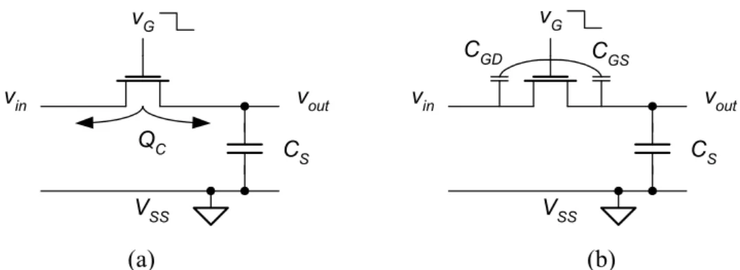
Figure 3.1: Basic sampling circuit... 34
Figure 3.2: (a) Gate, drain-to-source and output voltages; (b) Conductance and inverse of drain-to-source resistance... 35
Figure 3.3: Waveforms with increased gate voltage; (a) Gate, drain-to-source and output voltages; (b) Conductance and inverse of drain-to-source resistance. ... 35
Figure 3.4: MOS capacitances illustration. ... 38
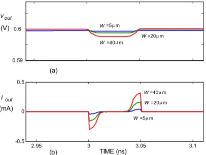
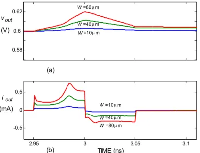
Figure 3.5: Changing switch aspect ratio; (a) Output voltage; (b) output current... 40
Figure 3.6: Switch turning-OFF period; (a) Output voltage; (b) Output current. ... 40
Figure 3.7: (a) Gate-to-source and gate-to-drain capacitance; (b) Sum and total gate capacitance... 41
Figure 3.8: Dummy switch implementation. ... 45
Figure 3.9: Switch turning-OFF period, with dummy switch; (a) Output voltage; (b) Output current... 45
Figure 3.10: Bottom-plate sampling implementation in a S/H... 46
Figure 3.11: Switch turning-OFF period with top-plate sampling switch; (a) Output voltage; (b) Output current. ... 47
Figure 3.12: Dickson multiplier circuit [48]... 48
Figure 3.13: Voltage doubler circuit. ... 50
Figure 3.14: Changing the aspect ratio; (a) Conductance; (b) Output voltage... 53
Figure 3.15: Bulk-switching circuit applied to M1. ... 55
Figure 3.16: Sampling circuit with a CMOS switch. ... 56
Figure 3.17: (a) Individual and equivalent conductances of a CMOS switch; (b) Output voltage. ... 56
Injected output current... 59 Figure 3.20: CMOS with small input voltage; (a) Output voltage error; (b) Injected current... 59 Figure 4.1: Sampling circuit; (a) Diagram with NMOS device; (b) Equivalent charging circuit. ... 66 Figure 4.2: Sampling circuit during device turn-off; (a) Charge injection; (b) Presence of parasitic capacitance... 67 Figure 4.3: Flip-around S/H circuit. ... 68 Figure 4.4: Double sampling S/H circuit... 69 Figure 4.5: Charge redistribution S/H circuit. ... 70 Figure 4.6: Passive S/H with source follower. ... 72 Figure 4.7: Passive S/H with improved (enhanced) source follower. ... 73 Figure 4.8: Pipelined converter stage. ... 73 Figure 4.9: Detail of closed-loop stage switches... 74 Figure 4.10: Closed-loop amplifier connections. ... 77 Figure 4.11: Open-loop structured stage. ... 80 Figure 4.12: Open-loop amplifier during amplification phase. ... 80 Figure 4.13: Open-loop structured 1.5-bit stage amplifier. ... 82 Figure 4.14: Degenerated differential pair amplifier... 83 Figure 4.15: Amplifier with mirrored current. ... 84 Figure 4.16: Amplifier with super source followers. ... 85 Figure 4.17: Amplifier with internal feedback. ... 85 Figure 4.18: Amplifier with local feedback. ... 86 Figure 4.19: Residue amplification errors; (a) offset; (b) gain; (c) nonlinearity... 88 Figure 4.20: Ideal and obtained output responses; (a) ending period; (b) starting period... 89 Figure 4.21: Sampling circuit with four switches. ... 90 Figure 4.22: Control signals sequence... 91 Figure 4.23: Sampling circuit with parasitic capacitances. ... 91 Figure 4.24: Equivalent circuit during S1 turn-OFF. ... 92
Figure 4.25: equivalent circuit during S2 turn-OFF... 92
Figure 4.26: Equivalent circuit during S3 turn-ON... 93
(b) Switch conductance. ... 105 Figure 5.7: NMOS bootstrapping circuit simulated results with oversized capacitors; (a) Input and gate voltages; (b) Switch conductance. ... 105 Figure 5.8: Differential bootstrapped scheme; (a) Partial conductances of the stages; (b) Equivalent conductance of global circuit. ... 106 Figure 5.9: Bootstrapping circuit without voltage doubler [76]... 107 Figure 5.10: PMOS bootstrapping circuit diagram ... 108 Figure 5.11: PMOS bootstrapping circuit diagram. ... 108 Figure 5.12: PMOS bootstrapping circuit simulated results; (a) Input and gate voltages; (b) Switch conductance ... 109 Figure 5.13: S/H circuit with feedback loop and with high input impedance [80]. ... 110 Figure 5.14: S/H circuit with capacitor placed in the feedback path [80]. ... 111 Figure 5.15: Output stage of an amplifier. ... 112 Figure 5.16: Representation of a SO based block. ... 113 Figure 5.17: SO clock signals sequence. ... 113 Figure 5.18: NMOS sampling circuit with input voltage fall; (a) Gate and output voltages; (b) Input and gate-to-drain voltages... 117 Figure 5.19: CMOS and parasitic transistors. ... 118 Figure 5.20: Changes in the NMOS, PMOS and equivalent (gEQ) switches conductances using the proposed technique versus input signal. ... 119 Figure 5.21: n-type and p-type SLC simplified schematic... 121 Figure 5.22: n-type and p-type SLC practical realization. ... 124 Figure 5.23: Simplified flow-chart of the main steps to optimize the sizing the auxiliary capacitors used in the SLCn and SLCp circuits. ... 125 Figure 5.24: Flipped-Around S/H Circuit. Four different SLC or CBT circuits are required to drive the four switches in the signal path... 127 Figure 5.25: THD of a fully-differential flip-around S/H circuit for the 4 different techniques versus input signal frequency. ... 127 Figure 5.26: THD obtained for 4.7 MHz and large amplitude input signal. ... 128 Figure 5.27: THD obtained for different main switches size. ... 129 Figure 5.28: Gate voltages applied to the main switches for a ± 0.5Vpp input signal
voltages... 140 Figure 6.6: Ability of discharging the sample capacitor, Qv (normalized), as function of
VDD and fall time, t... 141 Figure 6.7: 10-bit pipelined A/D architecture. ... 142 Figure 6.8: SO/CBT realization of the S/H. ... 143 Figure 6.9: SO realization of the 2.5-bit MDACs. ... 144 Figure 6.10: Simulated results of the digital output of the ADC with VDD =1.5 V; (a) using the conventional clock generator; (b) using the proposed single-phase scheme. ... 146 Figure 6.11: Simulated SFDR versus supply voltage (VDD) when using the conventional or the single phase scheme. ... 147 Figure 6.12: Expected ENOB values versus supply voltage (VDD) when using the conventional or the single phase scheme... 148 Figure 6.13: Block diagram of the architecture of the 6-bit 2-channel time-interleaved pipelined ADC... 151 Figure 6.14: Control clock signals and corresponding ADC architecture timing. ... 152 Figure 6.15: Clock signals generation. ... 153 Figure 6.16: S/H block diagram. ... 154 Figure 6.17: Schematic of the SLC circuit, single-phase controlled, used to linearize the CMOS (ATG type) input switches (M1 and M2)... 155
List of tables
1.1.
Motivation for the Thesis
The development of analog electronics during the last years has been majority pushed by the extensive proliferation of wireless communication and multimedia devices. The reduced power dissipation, while assuring the necessary high speed operation, is a mandatory goal in any electronic circuit design, more relevant when battery-powered. Moreover, also the size, weight, reliability, security and price are decisive in the devices design. Therefore, the technologies and the techniques have been pressed to answer to those challenges, with improved, efficient and secure solutions.
The complementary metal-oxide-semiconductor (CMOS) architecture has been the prevailing technology used in integrated circuits, for more than 30 years. The major reason for the success of the metal-oxide-semiconductor (MOS) transistor is the fact that it is technology possible to scale it to increasingly smaller dimensions, decreasing the transistor delay times and increasing the circuit performance. However, even though new integrated circuits technologies and techniques can offer high speed of operation, the power dissipated is frequently unable to fulfill the restrictions and demands imposed by the applications. Moreover, the continuous downsizing is putting in evidence, once again, some reliability questions thought as already answered till now.
The switched-capacitor (SC) has been the current design technique used in analog integrated circuits. SC circuits comprise capacitors, switches and amplifiers. Researchers and designers have been, and will be, developing these areas. The metal-oxide-metal (MoM) capacitors are getting more and more efficient in terms of capacitance per unit area. The metal-insulator-metal (MiM) capacitors can be avoided and, hence, pure cheaper logic processes can be used to design low-cost mixed-mode circuits. Moreover, matching is quite stable. The areas that can drive to design improvements with greater impact, while preserving the simplicity of the layout, are the switches and amplifiers.
The amount of charge destroyed in SC circuits, by having overlapping clocks, is getting smaller for the same switches sizing, due to the faster transition times of the CMOS gates. Therefore, the single-phase technique, addressed in this Thesis, can be applied to many SC circuits, simplifying the circuit layout.
The linearity performance of the switches in rail-to-rail operation is degrading since the threshold voltage is not scaling down proportionality to the power supply voltage reductions. Even so, the standby power and the active power ratio have been increasing. The reduced lowering of the threshold voltage decreases the gate overdrive, and therefore, the switches performance. Attempts to overdrive the gate voltage are limited by the stress over the gate and by reliability constraints. The oxide thickness has been scaled approximately proportional with the length, maintaining the ability of gate control through the scaling levels. More, as the scaling of the voltages is not as fast as the scaling of the dimensions, the applied electric field has increased and the time dependent dielectric breakdown has decreased. Even maintaining the electric field value, as the dielectric breakdown becomes a function of the voltage per si, the reliability issue is of the major importance when voltage overdrive techniques are used. Alternatively, a novel switch-linearization solution is proposed in this Thesis and demonstrated in silicon in a 10-bit analog-to-digital converter (ADC).
order to avoid the need of any kind of calibration. This approach is proposed in this Thesis for the first time, and demonstrated through electrical simulations of a 6-bit 1GS/s ADC.
Table 1.1 summarizes the major Pros and Cons of designing SC circuits in sub-micron technologies. Notice that the Pros/Cons referred with an (*) are addressed and explored throughout in this Thesis, by proposing new and efficient solutions to deal with.
Table 1.1: Pros and Cons of designing SC circuits in advanced sub-micron technologies.
Pros Cons The frequency of operation is improving due
to the reduction of the minimum channel length size.
Variability pushes the channel thermal noise and the induced gate noise correlation to be an important limitation.
Due to the fast transition times, the amount of charge destroyed by having overlapping clocks is getting smaller for the same switches sizing. (*)
The continuous reduction of the channel length underlines the importance of the saturation velocity limitation, output resistance and intrinsic gain reduction. (*)
Matching of transistors is slightly improving. Matching of capacitors is stable in the 10-11 bits range.
Open-loop gain of amplifiers over PVT corners, specially at high temperatures, is subject to huge degradations. (*)
MoM capacitors are getting more and more efficient in terms of capacitance per unity area. No MiM capacitors are required and, hence, pure Logic Processes can be used to design low-cost mixed-mode circuits.
Leakage currents are increasing and becoming more important, specially the OFF-state current due to threshold scaling, and the gate tunneling current due to oxide thickness reduction.
New technology options of materials and structures are being investigated.
Linearity performance of switches in rail-to-rail operation is degrading since threshold voltage is not scaling proportionally. (*) Modeling is following the needs. Holistic
models have been developed for accurate noise modeling.
1.2.
Research contribution
The research work presented in this dissertation lead to the following original contributions:
1) A new switch-linearization circuit (SLC), which provides the necessary control voltages to the switches to guarantee the linear behavior without overstressing the gate. Part of the results of this development can be found in [1][2][3][4].
2) A new combination of open-loop amplification structures using amplifiers with local-feedback, with increased power efficiency and avoiding the need of additional calibration or correcting schemes. Part of this development can be found in [5][6].
3) The application for the first time of a single-phase technique to pipelined ADC, simplifying the circuit while maintaining the signal integrity and the overall performance when compared with conventional clock scheme. Part of this development is available in [7][8].
Two different integrated prototypes were fully designed and electrically simulated (over PVT corners) at transistor level1: 1) A two-channel time interleaved 6-bit 1GS/s pipelined ADC based on open-loop amplification using amplifiers with local feedback and employing the simplified single-phase scheme (applied to pipelined ADCs for the first time) and the proposed new SLC circuits; 2) A 10-bit 4-to-32MS/s pipelined ADC, again using the proposed new SLC circuits in the front-end sample-and-hold (S/H) and employing, as well, the referred single-phase scheme. However, due to the following factors only the second prototype was laid out, fabricated and experimentally evaluated: i) due to the limited time for pursuing the Ph. D. degree, it would be possible to design a single prototype integrated circuit; ii) it would be convenient to demonstrate the performance of the new SLC circuits at higher resolutions (this is, in fact the most original contribution of this Thesis). Hence it was preferred the 10-bit ADC rather than the 6-bit resolution one. Since it would be possible to test the 10-bit ADC also in sub-sampling mode, we would be able (as we did in fact) to
1
extend the signal frequency range to quite high values; iii) even if the 6-bit 1GS/s was fabricated, we would not be able to test it since, on the one hand, the available logic analyzer in the laboratory had a limited maximum acquisition frequency of 200 MS/s and, on the other hand, a complete new pad ring with high-speed, low-noise performance and with dedicated electrostatic discharge (ESD) protections would be necessary to be designed (and this is not an easy task unless for experienced I/O-pad designers) and, moreover, 3.3V or 2.5V LVDS output drivers would also to be designed from scratch in order to reach the desired 1GHz conversion rate. In conclusion, the 6-bit ADC would be much more risky to be integrated and experimentally evaluated (specially due to the testing environment and auxiliary testing structures) than the 10-bit ADC integrated circuit.
1.3.
Structure of the Thesis
This Thesis is organized in eight Chapters. The first one is the present introduction, beginning with the presentation of the context, and revealing the motivation that is the cause of this research work. After, the major original contributions are mentioned, and the structure of this dissertation is pointed out.
The second Chapter presents an overview of the technology scaling and its impact in the devices and circuits characteristics. The power dissipation, the conductance, the gain, the speed and noise are analyzed, and the different sources of leakage are detailed.
The third Chapter is focused in the non-ideal behavior of the switches, a major problem to be solved in low-voltage implementations of SC circuits. The main sources of error are analyzed in detail, as conductance nonlinearity, charge injection and clock feed-through. Also, the switch controllability is questioned, considering the threshold and overdrive levels.
The fifth Chapter is a systematic presentation of conventional solutions to minimize the non-ideal behavior of the switches, ending with the proposal of a new switch-linearization technique. The bootstrapping and the switched-OpAmp (SO) techniques are dissected. Moreover, before being the new solution presented and deeply explained, the reliability issue of the switches is discussed in detail, clearly anticipating the usefulness and need of the proposed technique.
The sixth Chapter describes the electrical design of two ADC, using the solutions discussed and proposed in the previous Chapters. The first example, described in the first Section, is centered in the phase complexity problem, analyzing the possibility of application of the single-phase technique to medium resolution pipelined ADCs. The second design, described in the second Section, explores the characteristics of the passive sample-and-hold, of an amplifier employing local-feedback topologies and of the proposed switch-linearization circuit technique, in the design of a low resolution and high sampling rate complete pipelined ADC, with open-loop residue amplification structure.
The seventh Chapter presents the practical realization of a pipelined ADC in integrated circuit. The description of the design is focused on the front-end S/H circuit, where the proposed new SLC circuits are used. The realization of the SLC circuits for the particular S/H, with multiple sampling switches, is described, and the linearity of the switches over rail-to-rail signal swings is confirmed by the measured results. Also, the non-existence of stress over the gate is guaranteed.
2.
Switched-capacitor circuits in deep-submicron CMOS
The scaling of metal-oxide-semiconductor (MOS) devices has stimulated new applications with remarkable improvements in cost, speed and power dissipation. In turn, the success of such improvements is pushing the technology towards new and continuous advances, which are taken for sure and granted. The expectation is high, and the density and speed of the integrated circuits (IC) are believed to increase, however the challenges of the scaling are increasing in number and complexity.
2.1.
Technology scaling
During the last four decades the industry has developed new IC process technologies and products. Each generation of process technology has doubled the transistor density, with a reduction of feature size to, approximately, 0.7. Till the 1990’s, a new technology generation has been introduced every 3 years, resulting in the double of transistor density achieved every 3 years2. Figure 2.1 [9] shows the Intel feature size (metal line width) reduction over the last decades, in particular a reduction of 0.7 raised to the power of 7, during the early 7 technology generations, over one period of 21 years. The late technology generations have been introduced every 2 years, and the downscaling has been accelerated. The MOS gate lengths have been scaling down faster than the other feature sizes, as also shown in Figure 2.1.
1970 1980 1990 2000 2010
10-2 10-1 100 101
YEAR
S
IZ
E
(
m
)
technology generation
gate length
Figure 2.1: Feature size scaling [9].
Scaling so fast and so deeply has exposed new problems and constraints, solutions have been demanded, and questions about the end of MOS scaling have been placed more frequently. But the growing challenges and problems have been analyzed, numerous solutions are being proposed and presented, and the end is not yet in sight.
2
The transistor or circuit parameter changes constant electric-field (CE) scaling were analyzed in detail in [10], and Table 2.1 reproduces the summarizing table, being k the scaling step. The CE scaling involves supply voltage and device dimensions scaling, being reduced by 1/k, preserving the same electric-field in the new downscaled device.
Table 2.1: Scaling results for circuit performance [10]. Device or Circuit Parameter Scaling Factor
Device dimension 1/k
Doping concentration k
Voltage 1/k
Current 1/k
Capacitance 1/k
Delay time per circuit 1/k
Power dissipation per circuit 1/k2
Power density 1
The CE scaling results in a reduction of the current, also by 1/k, and subsequently the power dissipation is reduced by 1/k2 and the resistance is not changing. The area is also reduced by 1/k2 and, as the thickness of insulating films is reduced by 1/k, the devices capacitances are only reduced by 1/k and the dynamic power dissipation by 1/k3. Therefore, as the resistance is constant, the delay time is reduced also by 1/k.
As stated in [10], one area in which the device characteristics fail to scale is in the sub-threshold or weak inversion region of the turn-on characteristic. Below sub-threshold, the current is exponentially dependent on the gate voltage, with an inverse semi-logarithmic slope that should be maintained. It was expected, as long as the tolerance spreads on the threshold voltage are also proportionally reduced, the CE scaled circuits operate properly at lower voltages.
1/k. Also, the area mismatch is increased if the parameter fluctuations are not reduced with the downscaling.
The peculiar difficulties found with MOS devices threshold voltage scaling, and in keeping the adequate signal swing, and the degradation of some key parameters, forced the use of a constant voltage (CV) scaling rule, prior to the 0.5 μm technology. The supply and threshold voltages, VDD and VT, the oxide thickness tox and the matching parameter AVT, are shown, for different technologies, in Figure 2.2 [12]. With CV scaling the doping concentration is increased by k2, and the current and electric-field by k. Also, the power dissipation is increased by k and the dynamic power reduced only by 1/k. The transconductance and DR are maintained, while the maximum transconductance and the delay time are improved. The improvements are supported in the power increase and also in the reliability degradation. In fact, in the CV scaling, the higher electric-field causes life span reduction, due to hot carriers and oxide breakdown.
0.1 1
0.1 1 10
DD
V
T
V
ox
t
A
VT
100
10 1000
TECHNOLOGY NODE ( m)
(V
)
(A
)
(m
V
. m
)
o
Figure 2.2: Supply and threshold voltages, thickness and matching parameter for different technologies [12].
More recently, however, the CE rule seems to have reached the lower limits of threshold voltage scaling. It was assumed [10] that the threshold voltage would scale together the supply voltage, while maintaining available the control capability over the device gate and improving the power and overall performance. However, after three decades of continuous scaling the sub-threshold leakage has increased from levels lower than 10-10 A/mm up to 10-7 A/μm [9] and, therefore, is nowadays a major limitation or constraint for deeper scaling. This is the main reason why, in deep-submicron technologies (beyond 90 nm) the “flavour” of high threshold devices is provided by the foundries.
Another assumption in CE scaling is the ability of continuously reduce the gate oxide thickness. The capacity of lowering the gate oxide thickness has contribute to the scaling success, however has reached only a few atomic layers, which can be close to the limit. Not only further thickness scaling is difficult, also the consequent gate-oxide leakage current increase, due to direct tunneling, becomes more complex to be handled and controlled.
Moreover, the CE scaling rule assumed that channel doping concentration could be continually increased, to attain threshold voltages and to limit short channel effects. However, when channel doping concentration gets too high, the proximity of the valence and conduction bands in the depletion region of the junctions causes a direct band-to-band tunneling leakage current, and an additional increase in the overall leakage current and power.
Other important issue is the interconnection lines scaling. When scaling the thickness and the width, the cross-sectional area is reduced by 1/k2. It is expected that the length is also scaled with a factor close to 1/k, therefore the resistance is increased, approximately by k, as shown in Table 2.2 [10].
Table 2.2: Scaling Results for Interconnection Lines [10].
Parameter Scaling Factor
Line resistance k
Normalized voltage drop k
Line response time 1
Being the current also scaled, by 1/k, the first conclusion is the current density is increased by
k, which causes a reliability constraint. The other conclusion is that the voltage drop is maintained; however, as the voltage is decreased by 1/k, the relative or normalized voltage drop is increased. Furthermore, the response time is maintained, which can be considered, relatively to the improvement in delay time of the scaled devices, not appropriated or even inadequate when complex layouts and long interconnection lines are used.
2.2.
Achievable SNR and power dissipation
One major challenge for implementing precision analog circuitry in deeply scaled processes is the reduction of supply voltages. Lower supply voltages imply lower available voltage swings and limited signal-to-noise ratio (SNR). With reduced swings, and in order to maintain the dynamic-range in a noise limited circuit, the circuit noise should also be reduced [13], which requires, in a switched-capacitor (SC) circuit, the selection of a capacitor with increased size to lower the thermal noise. Increasing the capacitor size denotes a power dissipation cost.
Power dissipation of analog circuits is proportional to the level of signal integrity (SNR) and to the signal frequency, fin [14]. For a simple circuit (class-A) driving a load capacitor C, the integrated thermal noise, rms2 , and the bias current, iDS, can be expressed by (2.1) and (2.2), with k the Boltzmann constant, T the temperature and Ain the input signal amplitude.
C kT
rms
2
(2.1)
in in DS f CA
i 2 (2.2)
Introducing the voltage efficiency ηv = Ain/VDD, and the current efficiency ηc = iDS/IDD, the minimum power P can be expressed as a function of the SNR (the input signal and noise power ratio) by (2.3).
SNR Tf
P in
c v
1
More performance comes at the cost of increased current consumption. The power dissipation is technology independent, as long the voltage and current efficiency is maintained. Relation (2.3) is changed and become more explicit for the case of a transconductance amplifier operating linearly [15][16]. Assuming the MOS square law (and neglecting any body effect), the necessary transconductance, gm, and the effective gate overdrive voltage, vGSeff, can be expressed by (2.4) and (2.5).
C f
gm 2 in (2.4)
m DS GSeff
g i
v 2 (2.5)
Therefore, the power relation with frequency and SNR can be expressed by (2.6), presenting explicitly the supply voltage and the gate overdrive voltage.
DD GSeff in
c
v V
v SNR Tf P
2
1
(2.6)
The minimum power dissipation increases with decreasing supply voltage. Similar result is obtained for other thermal noise models [14][17]. Figure 2.3 shows [14] the power for a simple voltage buffer, with fixed topology and performance, for different supply voltages and technologies. The bold circles correspond to the use of the nominal supply voltage of the specific technology.
The minimum power dissipation increases with decreasing supply voltage over the same technology, and also with newer technologies at nominal voltage [14][18]. However, maintaining the supply voltage for different technologies, the newer requires lower power.
1 2
PO
W
ER
(V) 130 nm
180 nm 90 nm
250 nm
DD
V
Figure 2.3: Power for a simple buffer, for different supply voltages and technologies [14].
Considering only the threshold voltage mismatch, and accepting that the voltage mismatch,
VT
, is reported to scale as the oxide thickness, as shown in Figure 2.2, and to the inverse of the square root of the gate area, length (L) and width (W) product, as in (2.7), the minimum gate area for an imposed SNR can be expressed by (2.8) [12].
oxeff
VT t
WL
1
(2.7)
SNR t
V WL oxeff
DD v
2 2 2
1
(2.8)
The minimum gate capacitance Cg, for the particular required accuracy, can be obtained, apart from the dielectric constants, dividing the area by the oxide thickness, as in (2.9).
SNR t
V C oxeff
DD v g 2 2
1
(2.9)
The necessary current to support the input voltage swing, with amplitude Ain and frequency
SNR f t V
I oxeff in
DD v DD
c
1 (2.10)
Therefore, the power dissipation can be expressed by (2.11).
SNR f t P oxeff in
c v
1
(2.11)
This derived expression points to a decrease of power when the oxide thickness is scaled down, and the voltage and current efficiency are maintained, in circuits where the mismatch is dominant. This result also indicates and confirms the existence of one extra power dissipation margin in certain circuits with scaled devices. These are the circuits requiring low resolution, when the value of the capacitor is determined by other constraints such as stability or matching, and that value is higher than the required by the thermal noise limitation. In this case it results in a power and area scaling trend similar to that of the digital circuits with constant speed [13]. The high resolution circuits still are dominated by the thermal noise. The diverging zone seems to be around the 55 to 65 dB [13], but also seems to be moving up with new technologies and circuits [15].
Also is relevant the voltage and current utilization factors. Newer designs are optimized to accommodate larger signal swings and to be more efficient in the current use.
2.3.
MOS switches
An analog switch must present a low and linear ON-resistance for a large signal swing. The drain-to-source conductance, gDS, of a MOS switch operating in the linear region is a function of the mobility in the channel, μ, the oxide capacitance per unit area, Cox, the gate width and length, W and L, the gate-to-source voltage, vGS, the threshold voltage, VT, as represented by (2.12).
GS T
ox
DS v V
L W C
Scaling the device and lowering the oxide thickness, the capacitance per unit area is increased pointing to an increased conductance. However, that is canceled by the variation of the last term, the effective gate voltage. Considering that both the gate-to-source and the threshold voltages are lowered by 1/k, the conductance is also lowered by 1/k. More, as the threshold voltage is not scaling as fast as the supply and available gate-to-source voltages, the conductance is deteriorating with scaling.
Not only the achievable maximum conductance is reduced, also the linearity of the conductance is highly reduced with supply voltage, as the relatively increased threshold voltage is shrinking even more the signal amplitude span. That fact forces the use of very low signal levels and the use of common-mode signal levels close to one of the supply rails. Moreover, the body effect implies a threshold voltage variation, additionally increasing it for signal (source-to-bulk) increased voltages, and reducing even more the signal swing. In particular, the conductance of the switches used in sample-and-hold circuits operating at lower supply voltages, is more and more signal dependent.
Another challenge for highly scaled MOS devices is reducing the parasitic series source and drain resistances to tolerable values with very shallow source and drain junction depth [19]. One of the main novel aspects treated in this Thesis deals with how to solve the lack of linearity of the switches on deep-submicron CMOS.
2.4.
Intrinsic gain and frequency of operation
DS
i L DD T V e
V /
(2.13)
Increasing the current or decreasing the length implies a reduction of gate control. Also the intrinsic voltage gain, the output resistance and transconductance product, is reduced.
Moreover, for very short channel lengths, the transconductance is limited by the velocity saturation. Therefore, devices from newer technologies show degraded voltage gain, even when the supply voltage is maintained. For scaled supply and threshold voltages, the gain lost is even deeper. At circuit level that lower performance can be compensated by techniques that boost the gain, such as cascoding, however it is difficult to fit within the allowed range left by the decreased supply voltage, and multi-stage (e.g. 3-stages) amplifiers become an alternative, more and more frequent.
Also, in scaled devices the transconductance-current ratio is not improving, as a function of effective gate voltage [15][21]. However, a higher transconductance-current ratio is achievable by new technology devices for the same operating frequency [15]. The frequency performance of devices improves with scaling. Considering the gate capacitance Cg is the product of area and capacitance per unit area, and assuming for simplicity the transconductance in strong inversion is as in (2.14), the maximum operating frequency fin of the operation of the device is expressed as in (2.15).
GS T
ox
m v V
L W C
g (2.14)
) (
2 1 2
1
2 GS T
g m
in v V
L C
g
f
(2.15)
For different technologies with the same channel length, the maximum frequency hardly changes, and it is a function, apart from the mobility variation, of the effective gate voltage. However, reducing the length by 1/k, equation (2.15) points to an increase of the maximum frequency by k2.
the velocity saturation vsat, [20][22] as the transconductance is reduced to (2.16), and therefore, the maximum frequency is not any more a function of the effective gate voltage, resulting in equation (2.17).
sat ox m C Wv
g (2.16)
L v
f sat
in
2 1
(2.17)
The maximum voltage gain, G, obtained in the case of infinite output impedance, is expressed as the ratio of the saturation transconductance, gm, and the output conductance in saturation,
gDS, as in (2.18).
DS
i L DS
m e
g g
G /
(2.18)
To increase the gain it is needed to increase the channel length or to reduce the current iDS. In order to cancel the length scaling effect on the gain, the current and the drain control over the current must be also scaled. Therefore, the drain junction and depletion depths must be reduced, to reduce the size of the drain electrode and to introduce a shielding effect with the substrate region, and, most important, the oxide thickness must be reduced to increase the gate control (and the gate capacitance value).
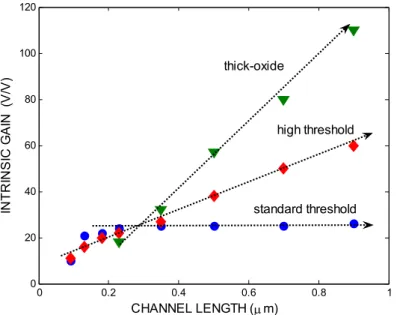
In Figure 2.4 is shown the effect of the channel length value in the intrinsic gain of a device, in a 90 nm technology. For the standard devices (standard threshold voltage), the increase of the intrinsic gain by increasing the length (as discussed before) is limited to a narrow range close to the regular length of the technology. Increasing more the channel length, has not any effect in the intrinsic gain value. One way to overcome the degradation of the gain is to use thick-oxide or high threshold devices. In Figure 2.4 is also shown the intrinsic gain of both types of device for different channel lengths, with the same technology. It is possible to increase the gain by a factor of 2, 3 or 4, by using alternative devices. Also, the thick-oxide devices can operate at high supply voltages, improving the power dissipation and the voltage swing. However, the frequency of operation is reduced, forcing to a limited use. In order to benefit from the best that technology scaling can provide, mixed device types or compound structures can be used. The use of high voltage and low leakage thick-oxide devices in certain blocks, can be combined with the use of high speed and improved matching thin-oxide devices in other blocks of the same circuit.
0 0.2 0.4 0.6 0.8 1
0 20 40 60 80 100 120
CHANNEL LENGTH ( m)
IN
T
R
IN
S
IC
GA
IN
(
V
/V
)
high threshold
standard threshold thick-oxide
Figure 2.4: Intrinsic gain as a function of channel length, for standard, high threshold and thick-oxide devices.
2.5.
Device leakage
The device leakage issue can be divided in three different areas, corresponding to three different sources of leakage, which relative importance is changing as devices are deeply scaled: junction leakage, gate leakage and OFF-state leakage.
The junction leakage arises from the high doping concentration in the channel region, increased to attain threshold voltages and to limit short channel effects in aggressively scaled devices. The proximity of the valence and conduction bands in the depletion region of the junctions causes a parasitic tunneling current, the gate induced drain leakage (GIDL) current
Ij. Although the leakage is high (approximately 1 nA/μm with L = 30 nm and 1 V reverse bias) is one to two orders of magnitude smaller relatively to the other leakages [25]. Also, when projecting the increase in doping for the next generation scaled devices, as depicted and identified by the gate length in Figure 2.5 [25], still it will be lower.
0 5 10 15 20
10-12 10-11 10-10 10-9 10-8 10-7 10-6
(
A
/ m)
DOPING CONCENTRATION (10/cm )
j
3
10 nm
15 nm 20 nm
I
Figure 2.5: Junction leakage for different doping concentrations (1 V reverse bias) [25].
the control over the gate and to minimize the sub-threshold current is pushing the oxide scaling to continue or, in alternative, to use high-K dielectrics for MOS device applications and to apply multi-layer dielectric stacks, presently an area of active research and development. Figure 2.6 shows the gate leakage current Ig, as a function of the equivalent oxide thickness value EOT, for high-K dielectrics and oxide, with 1 V bias [25].
The recent BSIM4 gate tunneling model includes the gate current between the gate and the substrate, the current between the gate and the channel, being this partitioned between both the source and the drain, and the current between the gate and the diffusion regions [23][24]. BSIM4 also includes the equivalent oxide thickness parameter EOT, to be used for non-oxide gate insulators.
5 10 15 20 25
1E-6 1E-5 1E-4 1E-3 1E-2 1E-1 1E+0 1E+1 1E+2 1E+3 1E+4
g
(A
/c
m
)
(A ) High-K
SiO
2
o 2
I
EOT
Figure 2.6: Gate leakage as a function of the EOT, for high-K and oxide (1 V bias) [25].
Additionally to the power related to that significant value, another issue must be considered. With the higher relevance of the leakage current, the traditional gate capacitance must be considered to be in parallel to a tunnel conductance, gtunnel [14]. Both are area dependent, however the frequency associated to the parallel, fgate, is area independent, as in (2.19) for an NMOS case [14].
) 6 . 13 ( 2 16
510 . 1 2
toxeff vGS
GS g
tunnel
gate v e
C g f
(2.19)
This frequency defines the diverging point of capacitance or conductance preponderance; for lower frequencies the leakage current is dominant, and for higher frequencies the gate impedance is mainly capacitive and the device behaves as conventionally.
The thinner is the oxide, the higher is the frequency and the larger is the range of frequencies where the leakage current is dominant, possibly invading the workable frequency range. With thinner oxides, the gate current evaluation, iGS, becomes mandatory (2.20) [14], such as the current gain estimation, the drain and gate current ratio.
gate ox GS C WLf
i (2.20)
The transistor OFF-state leakage is perhaps the greatest problem facing continued scaling. As the transistor scales, the power supply voltage is scaled to maintain a moderate electric field and active power. The OFF-state power, the supply voltage and leakage current product, is not decreasing or even maintained. The leakage current is hugely increased by scaling, as the threshold voltage is reduced. Figure 2.7 shows the OFF-state leakage current, Ioff, as a function of the gate length, including for some research devices.
101 102 103 1E-13 1E-12 1E-11 1E-10 1E-9 1E-8 1E-7 1E-6 1E-5 1E-4 of f ( A / m )
GATE LENGTH (nm)
I
Figure 2.7: OFF-state leakage current for different gate lengths [25].
Below the threshold voltage, the drain-to-source current iDS, decreases exponentially with the gate-to-source voltage vGS, as in (2.21), where q is the unity charge, k is the Boltzmann constant, and sT represents the sub-threshold slope factor, which indicates the weight of the oxide capacitance compared with the bulk-to-channel capacitance [22].
kT s qv DS T GS
e
i
/ (2.21)Assuming the threshold voltage is defined as the gate voltage at which the drain current is 100 nA per unity geometry ratio W/L, equation (2.21) can be rewritten as (2.22), with the current in nA. nkT V v q DS T GS e L W
i ( )/
100
(2.22)
The OFF-state current (in nA) can be expressed by (2.23), being visible the dependency with the threshold voltage and with the temperature. The last justifies the frequent demands for the use of low temperature cooling of large ICs.
nkT qV off T e L W I / 100
2.6.
Devices variability and matching
Variability is an issue of major importance, while the scaling is pushing the technology to go faster and deeper. Uncertainty, after characterization, reduction and adaptation, results in variability. The new relevant properties of the researched devices are projected and measured, the manufacturing processes are controlled and improved, and new designs are adapted and innovated.
The relative spread or matching is, usually, a major limit of the achievable performance of analog circuits. With scaling, the channel doping has increased to undesirably levels in order to gain adequate control of short-channel effects and to set the threshold voltage properly. As a result, due to the small total number of dopants in the channel of extremely small MOS devices, the percent stochastic variation in the number and location of the dopants will increase, and this will sharply increase the statistical variability of the threshold voltage.
The variance of the change of the threshold voltage of different devices is proportional to the inverse of the area, and to the area proportionality constant for the threshold voltage, AVT [27][28]. The relative mismatch with the drain current (iDS) can be expressed as in (2.24)[14].
2
2 2
DS m VT
DS i
g WL A i
(2.24)
The factor AVT is assumed as proportional to the oxide thickness [12][14], as in Figure 2.2, being reduced by 1/k. However, this is canceled by the area scaling. The classical way to reduce mismatch is to enlarge the device, spending area and power. One option is to reduce the transconductance-current ratio.
proportional to the gate current with a proportionality constant XiGS, the total relative mismatch of the device current is as in (2.25) [14].
2 2 2 2 DS GS iGS DS m VT DS i i WL X i g WL A i (2.25)
This second term may increase with increased W and L, for large gate areas, resulting in an increased total relative mismatch of drain current differing from the usual expectation. However, reduction of mismatch can be achieved by increasing only the channel width, as both terms are improved [14].
Other issue related with the variability is the noise. The flicker noise or 1/f noise describes the quality of the conductive medium, and most of its power is concentrated at low frequencies. In a MOS device it is caused by the charge carriers in the channel getting trapped and later released, changing the carrier in number and mobility. The more homogeneous is the channel region, the lower is the flicker noise. The flicker noise does not depend on temperature, as the thermal noise does. It is proportional to the fabrication (homogeneousness) parameter, and to the inverse of area and frequency of operation. Then, scaling down the feature size and increasing the concentration forces to reconsider the importance and formulation of the flicker noise. BSIM4 offers an improved unified flicker noise model, which is smooth over all bias regions and considers the bulk charge effects [24].
The BSIM4 also offers an improved thermal noise model. Additionally to the charge-based model, the holistic model is provided, considering all the short-channel effects and velocity saturation effect. More, the noise-partition analysis unifies the induced gate noise and the channel noise with correlation [24]. The noise current through the gate capacitance, generated by the channel resistance high frequency noise, is now considered, such as its amplification.
2.7.
Conclusions
3.
Main challenge in the design of SC circuits in
3.1.
Introduction
Since the conductance of the switches is signal dependent, it becomes an important source of errors (e.g. causing harmonic distortion) in SC circuits, as the conductance settles the charging and discharging time constants. Attempts to minimize this particular error by oversizing the switches, not only contribute to a decrease of the efficiency, but also increase the charge injection when the switch turns OFF. Charge injection creates important offset errors as well as nonlinear errors, as it is not completely signal independent.
In this Chapter, the main non-idealities of the switches are described and analyzed in detail. Most relevant existing solutions are also presented.
3.2.
The switch conductance
In the linear region, for small signals, the metal-oxide-semiconductor (MOS) switch drain-to-source current, iDS, can be expressed by
DS DS TO GS ox
DS v
v V v L W C
i
2
(3.1)
It is a function of the mobility in the channel, μ, the oxide capacitance per unit area, Cox, the gate width and length, W and L, the gate-to-source voltage, vGS, the threshold voltage (assumed for simplicity to be constant), VTO, and the drain-to-source voltage, vDS. The switch drain-to-source conductance, gDS, is then represented by
GS TO DS
ox DS
DS
DS v V v
L W C v
i
g
(3.2)
gate-to-source voltage, vGSeff = vGS − VTO, in the form (3.3). The drain-to-source switch conductance value, and its variation with different variables and parameters, defines the SC circuit useful dynamic range (DR).
GSeff ox
DS v
L W C
g (3.3)
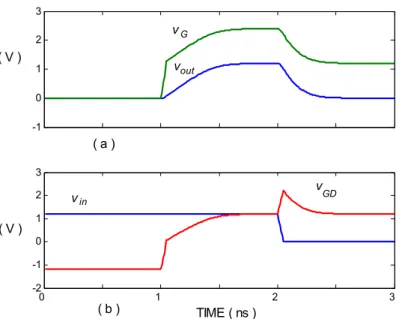
Figure 3.1 illustrates a simple SC circuit, such as a sample-and-hold (S/H) block. This S/H is electrically simulated using a standard 1.2 V 130 nm CMOS technology and BSIM3v3.4 models, being the NMOS device sized with aspect ratio 5/0.13, for a constant input voltage vin = 0.6 V, for a step voltage vG = 1.2 V with 50 ps rise time and applied between the gate and
VSS, the capacitor CS = 1 pF, initially discharged.
vin vout
vG
Vss
CS
Figure 3.1: Basic sampling circuit.
The capacitor is charged following an exponential (linear) response as illustrated in Figure 3.2(a). The capacitor voltage, vout item (a), ultimately (in infinite time) will reach the input voltage, vin.
Figure 3.2(a) illustrates the output voltage, vout item (b), if an ideal switch with such a conductance value is used, replacing the NMOS device. Then, in this case, the conductance value conduces to an over estimated value of the charging time.
0 0.5 1 1.5 2 (a) (b) (a)
0 1 2 3
0 2 4 6 8 10 12 (b) (V) (mS) TIME (ns) DS g DS v / DS i DS v out v v G
Figure 3.2: (a) Gate, drain-to-source and output voltages; (b) Conductance and inverse of drain-to-source resistance.
Figure 3.3(a) illustrates the case of the output response if the gate step voltage, with an overdrive voltage of 1.2 V, is applied between the gate and the input source.
0 0.5 1 1.5 2 (a) (b) (a) (b)
0 1 2 3
0 2 4 6 8 10 12 G v out v DS v (V) (mS) TIME (ns) DS g v /
DS DS
i
Because of the increased value of the effective gate-to-source voltage, the ratio iDS/vDS and the conductance gDS curves will converge to a final higher value, as shown in Figure 3.3(b). The capacitor will charge faster than in the previous example. However, if the final conductance value is used for an ideal switch, the output voltage, vout item (b), shows that, in this case, the use of the final conductance for the charging time calculation would conduce to a under estimated value.
Being, in certain cases, the calculation of the charging time a conservative approach, or an optimistic in other cases, the switch conductance is an important instrument to determine (and limit) the circuit response and performance. The relative error, ε, between the output, vout, and the input, vin, is an exponential function on the measuring time, usually half the period of the sampling frequency, FS, and the time constant. This error is given by (3.4), where CS represents the capacitance value of the sampling capacitor.
S S DS
C F g
e 2
(3.4)
The acceptable relative error for a desired number of bits accuracy, N, is given by
N
2
(3.5)
Then, the conductance can be defined as a direct function on the sampling frequency, accuracy, and sampling capacitance, in the form (3.6).
) 2 ln( 2C F N
gDS S S (3.6)
The conductance of the used switches is of the major importance, since it sets a limitation on the operating frequency3. As seen, the sampling process, not beginning always with the switch in the linear region of operation, will end with the lower possible drain-to-source voltage value and in the linear region.
3
Assuming the same sizing, to increase the conductance of the switch, and decrease the time constant, equation (3.3) indicates two possibilities: 1) up-scaling the switch device, increasing its ratio W/L; 2) increasing the effective gate-to-source voltage.
The first possibility will cause other problems, namely will increase the clock feed-through and the charge injection and also the load of the previous circuit (if it is the case). The second possibility can be achieved either by using higher gate voltages, or by reducing the threshold voltage.
The use of lower and lower values of supply voltages evidences the challenge to use those possible solutions. With reduced voltages, the feed-through phenomena is more problematic. Also the use of higher gate voltages is difficult and implies the use of voltage multipliers. Moreover, the threshold voltage values have also increased relatively to the supply voltage.
3.3.
The switch channel width scaling effects
Increasing the switches dimensions (W), will increase the clock feed-through and the charge injection. Charge injection is the process that occurs when the switches are turned OFF, of charging the capacitors in it’s vicinity by means of the charges stored in the switches channels, when they are in the ON state.
The clock feed-through, in the restrict sense, is the error added to the sampled voltage by the clock signal transitions due to the switches coupling capacitances. Those phenomena add errors to the sampled capacitor voltage. Furthermore, as the switches are turned ON and turned OFF periodically, the overall error can increase as a result of the accumulation of charges.
![Figure 2.2: Supply and threshold voltages, thickness and matching parameter for different technologies [12]](https://thumb-eu.123doks.com/thumbv2/123dok_br/16567270.737852/41.892.277.688.576.891/figure-threshold-voltages-thickness-matching-parameter-different-technologies.webp)
![Figure 2.3: Power for a simple buffer, for different supply voltages and technologies [14]](https://thumb-eu.123doks.com/thumbv2/123dok_br/16567270.737852/45.892.265.654.117.424/figure-power-simple-buffer-different-supply-voltages-technologies.webp)
![Figure 2.6: Gate leakage as a function of the EOT , for high-K and oxide (1 V bias) [25]](https://thumb-eu.123doks.com/thumbv2/123dok_br/16567270.737852/52.892.254.660.485.799/figure-gate-leakage-function-eot-high-oxide-bias.webp)