UNIVERSIDADE NOVA DE LISBOA
Faculdade de Ciências e Tecnologia
Departamento de Engenharia Electrotécnica e de Computadores
SI SC MDAC Switched Current-Capacitor
Multiplying Digital-to-Analog Converter
Por
João Rafael Caetano Pacheco
Dissertação apresentada na Faculdade de Ciências e Tecnologia
da Universidade Nova de Lisboa para a obtenção do grau de
Mestre em Engenharia Electrotécnica e de Computadores
Orientador: Doutor Nuno Paulino
Lisboa
3
Acknowledgments
It is a pleasure to thank to those who made this thesis possible.
First of all, it is difficult to overstate my gratitude to my thesis supervisor, Prof. Nuno Paulino, for
his support, availability and patience. Throughout the implementation period he provided another
point of view for problems that appeared during that phase.
I would also like to thank to Prof. João Goes and Ph.D. Michael Figueiredo for their support.
I am grateful to Prof. Rui Tavares for the several OPAMPs that he optimized for this dissertation.
It is also important to show him my gratitude for the IT support during server problems and work
area transference to the new server.
I am indebted to many of my colleagues for their, support me especially to those that shared two
offices with me.
Finally, I want to show a special gratitude to my family and friends for the unconditional support
they give me since the beginning of this dissertation.
4
5
UNIVERSIDADE NOVA DE LISBOA
Abstract
Faculdade de Ciências e Tecnologia
Departamento de Engenharia Electrotécnica e de Computadores
Mestre em Engenharia Electrotécnica e de Computadores
by João Rafael Caetano Pacheco
This thesis presents a 1.5‐bit MDAC circuit to be used in pipeline ADCs which employs a switched‐
current source to perform the reference shifting of the MDAC (the 1.5‐bit digital‐to‐analog function).
In the proposed circuit, the two single‐ended reference voltage sources that are traditionally used
( and ), are replaced by a switched‐current source. To evaluate and compare the
performance of the proposed circuit, two 10‐bit ADCs operating at 40 and 100MS/s, one using the
traditional switched‐capacitor (SC) MDAC and the other using the proposed MDAC, are designed.
At 40MS/s the simulation results show that the performance of the ADC with the proposed
MDAC is enhanced since the power needed for the current sources is smaller than the power
supplied by the reference voltage sources. Moreover, the proposed circuit does not require any
reference voltage buffer, which can be difficult to design with relatively low power dissipation.
With the removal of the required reference voltage buffer by means of the proposed circuit the
effects of the bonding wire in the normal operation of the circuit at high‐frequencies can be avoided.
This can be seen in the simulations results of the two designed 10‐bit 100MS/s pipeline ADC. They
have similar performance, but with high‐inductive bonding wires the proposed MDAC is not affected
6
7
UNIVERSIDADE NOVA DE LISBOA
Resumo
Faculdade de Ciências e Tecnologia
Departamento de Engenharia Electrotécnica e de Computadores
Mestre em Engenharia Electrotécnica e de Computadores
por João Rafael Caetano Pacheco
Esta tese apresenta um circuito MDAC de 1,5‐bit a ser usado num ADC pipeline que implementa,
através da comutação de uma fonte de corrente, o reference shifting de um MDAC (a função digital‐
to‐analog de 1,5‐bit). No circuito proposto, as duas tensões de referência single‐ended usadas
tradicionalmente ( e ) são substituídas por uma fonte de corrente comutada. Para avaliar e
comparar a performance do circuito proposto, foram desenvolvidos dois ADCs de 10‐bit operando a
50 e 100MS/s, um usando o tradicional switched‐capacitor (SC) MDAC e outro usando o MDAC
proposto.
Os resultados das simulações a 40MS/s mostram que a performance do ADC com o MDAC
proposto é melhorada, pois a potência necessária às fontes ou que passa pelas fontes pelas fontes de
corrente é menor que a potência fornecida pelas fontes das tensões de referência. Mais ainda, o
circuito proposto não necessita de qualquer tipo de buffer para as tensões de referência, que podem
ser difíceis de desenvolver tendo em vista uma baixa potência de consumo.
Com a remoção dos buffers das tensões de referência, através do uso do circuito proposto nas
condições de uma operação normal, os efeitos dos bonding wires a altas frequências podem ser
evitados. Isto pode verificado através dos resultados das simulações dos dois pipeline ADCs de 10‐bit
8
9
Content
Acknowledgments ... 3
Abstract ... 5
Resumo ... 7
List of Figures ... 13
List of Tables ... 18
Abbreviations ... 19
1 – Introduction ... 23
1.1 – Motivation and Context ... 23
1.2 – Comparison between Pipeline Architecture and others architectures ... 25
1.3 – Thesis Organization ... 29
2 – Pipeline ADC ... 31
2.1 – Introduction ... 31
2.2 – Pipeline ADC Architecture... 33
2.2.1 – MDAC ... 34
2.2.2 – Flash ADC ... 36
2.2.3 – Error sources in this Architecture ... 39
2.2.4 – Digital Correction ... 43
3 – Implementation of the Traditional Pipeline ADC ... 47
3.1 – MDAC ... 48
10
3.1.2 – Bootstrapping CMOS Switches ... 59
3.2 – 1,5‐bit Flash ADC ... 65
The block diagram of the Flash ADC is represented in the figure 3.2.1. ... 65
The Flash ADC consist of two comparators, thermometer‐to‐binary encoder and by an x, y and z encoder. The comparators used are based in ones of [17]. ... 65
3.2.1 – Comparator ... 66
The different values of capacitors in the switch capacity circuit will define the threshold level. So know the relation between them it will be used the two previous equations. The equivalence between them is: ... 67
The output of this circuit will by pre‐amplify and then the latch will decide the value of the thermometer. Because these ADC have low resolution the pre‐amplifier gain doesn’t need to be elevated, so the design of this circuit will be very simple. ... 68
3.2.2 – Digital thermometer and X, Y and Z encoder ... 68
3.3 – Final 2‐bit Flash ADC Stage ... 70
3.4 – Synchronization Logic ... 71
3.5 – Digital Correction Logic ... 73
3.6 – Simulations Results ... 74
4 – Proposed Pipeline ADC Architecture ... 77
4.1 – Overview of High‐Frequency Problems in Pipeline ADC ... 78
4.2 – Principle behind the new architecture ... 81
4.3 – The Current Switched MDAC ... 82
11
4.3.2 – Comparison between the OPAMP requirements in this new MDAC and the standard
MDAC ... 84
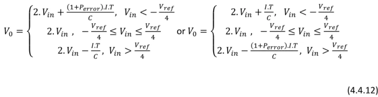
4.4 – The injected current error effects ... 88
4.5 – Implementation of the new Pipeline ADC ... 94
4.5.1 – The changes to the traditional MDAC ... 94
4.5.2 – The injection of current in the switched capacitor circuit ... 97
4.5.3 – The problem of the OPAMP sharing ... 108
4.5.4 – The OPAMP common‐mode problem ... 110
4.6 – Simulations Results ... 110
5 – Proposed Current Controller Architecture ... 114
5.1 – Overview ... 114
5.2 – Blocks of the Controller ... 115
5.2.1 – Scale Replica Stage ... 116
5.2.2 – Discrete Integrator ... 117
5.2.3 – Bias Circuit ... 121
5.2.4 – Current Controller Transfer Function ... 126
5.3 – Simulations Results ... 127
6 –Reference Voltage Circuitry ... 129
6.1 – Model used ... 130
6.2 – Simulations Results ... 144
7 – Conclusion and Future Work ... 149
12
A.1 – MIXDES 2011 ... 154
A.2 – ISCAS 2012 ... 160
Bibliography ... 167
13
List
of
Figures
Figure 1.2.1 – Flash ADC Architecture ... 13
Figure 1.2.2 – Pipeline ADC Architecture ... 14
Figure 1.2.3 – SAR ADC Architecture ... 14
Figure 1.2.4 – Sigma‐Delta ADC Architecture ... 15
Figure 1.2.5 – Two Step ADC Architecture ... 15
Figure 1.2.6 – Integrating ADC Architecture ... 16
Figure 2.2.1 – Block diagram of the Pipeline ADC architecture ... 21
Figure 2.2.1.1 – Generic MDAC structure ... 22
Figure 2.2.1.2 – Switched Capacitor Circuit adaptation in a MDAC using C‐DAC ... 22
Figure 2.2.2.1 – Flash ADC Architecture ... 24
Figure 2.2.2.2 – Switched‐capacitor based flash ADC Architecture ... 25
Figure 2.2.2.3 – Pipeline Stage Flash ADC Transfer Function without digital correction ... 26
Figure 2.2.2.4 – Pipeline Stage Flash ADC Transfer Function with digital correction ... 26
Figure 2.2.3.2.1 – Effect of the Comparator Offset on 1,5‐bit Stage Transfer Function ... 29
Figure 2.2.3.3.1 – Effect of Residue Amplifier Gain Error on 1,5‐bit Stage Transfer Function ... 29
Figure 2.2.3.3.2 – Effect of Residue Amplifier Gain Error on Pipeline ADC Transfer Function………30
Figure 2.2.4.1 – Pipeline stage operation: (a) ideal; (b) with comparator offset ... 32
Figure 3.1 – Trade‐off in the Pipeline ADC ... 34
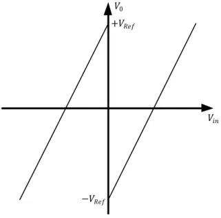
Figure 3.1.1 – Transfer function of a 1,5‐bit stage ... 36
Figure 3.1.2 –1,5‐bit pipeline stage structure ... 36
Figure 3.1.3 – Plot of capacitor thermal noise for a 10‐bit ADC ... 38
Figure 3.1.4 – Bode diagram of the transfer function of a single‐pole OPAMP ... 38
Figure 3.1.1.1 – OPAMP sharing technique ... 43
14
Figure 3.1.1.3 – Block schematic pipeline stage of the shared OPAMP ... 45
Figure 3.1.2.1 – Proposed bootstrapping for the CMOS switches ... 47
Figure 3.1.2.2 – Bootstrapping structure at different clock phases ... 48
Figure 3.1.2.3 – Proposed bootstrapping structure ... 50
Figure 3.2.1 – Block diagram of a 1,5‐bit Flash ADC ... 52
Figure 3.2.1.1 – Block diagram of a comparator ... 53
Figure 3.2.1.2 – Schematic of a comparator bank ... 53
Figure 3.2.2.1 – Digital thermometer and coding generation ... 55
Figure 3.2.2.2 – Logic circuit used for this encoder ... 56
Figure 3.3.1 – 2‐bit Flash ADC based in resistances ... 57
Figure 3.3.2 – Schematic of 2‐bit Flash ADC based in capacitors ... 57
Figure 3.2.2.2 – Logic circuit used for this encoder ... 58
Figure 3.4.1 – Pipeline output time division ... 59
Figure 3.4.2 – Stage’s output in time ... 59
Figure 3.5.1 – Digital Correction Logic digital domain ... 61
Figure 3.6.1 – Traditional ADC design output spectrum at F_S=40MS/s ... 62
Figure 4.1.2 – Example of a System‐On‐Chip ... 66
Figure 4.1.2 – Bond wire electrical model ... 67
Figure 4.2.1 – Injected current “trajectory” ... 68
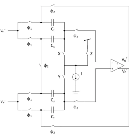
Figure 4.3.1 – Implementation of a CSMDAC’s injection zone ... 69
Figure 4.3.1.1 – Proposed 1,5‐bit MDAC stage ... 70
Figure 4.3.2.1 – Proposed 1,5‐bit MDAC stage during amplification phase ... 71
Figure 4.3.2.2 – Simple differential pair ... 72
Figure 4.3.2.3 – Simple representation of the problem ... 73
Figure 4.3.2.4 – Single‐ended representation ... 74
15
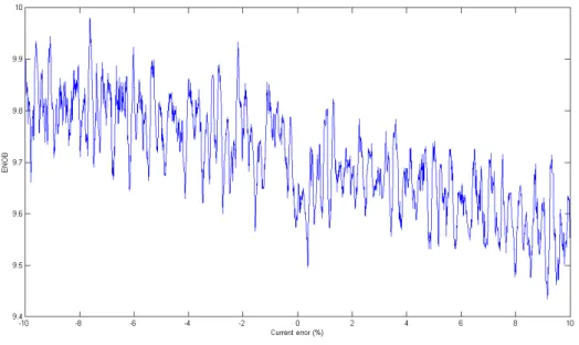
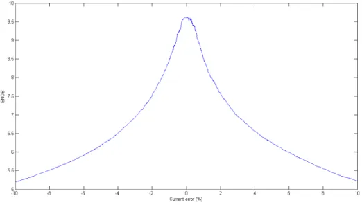
Figure 4.4.2 – ENOB of a current based system with a current error and a full scale input signal . 77
Figure 4.4.3 – ENOB of a current based system with a current error and an 80% full scale input
signal ... 78
Figure .4.4 – ENOB of a current based system with a current error and a full scale input signal ... 79
Figure 4.4.5 – ENOB of a current based system with a current error and an 80% full scale input signal ... 80
Figure 4.5.1.1 – Proposed 1,5‐bit MDAC architecture... 82
Figure 4.5.1.2 – Proposed 1,5‐bit MDAC architecture with the Flash ADC ... 83
Figure 4.5.1.3 – Unified digital thermometer with switch control ... 84
Figure 4.5.2.1 – Ideal time response of current based MDAC ... 85
Figure 4.5.1.3 – Unified digital thermometer with switch control ... 86
Figure 4.5.2.1 – Ideal time response of current based MDAC ... 87
Figure 4.5.2.2 – Channel charge injection ... 88
Figure 4.5.2.3 – Negative Feedback System representation ... 89
Figure 4.5.2.4 – Circuit’s time response stability ... 89
Figure 4.5.2.5 – The resistance presence in the feedback path ... 90
Figure 4.5.2.6 – Root‐locus ... 91
Figure 4.5.2.1.1 – Injector circuit ... 92
Figure 4.5.2.2.1 – Switches configuration ... 93
Figure 4.5.2.2.2 – NMOS switching configuration ... 93
Figure 4.5.2.2.3 – CMOS switching configuration ... 94
Figure 4.5.2.3.1 – Reducing the current injecting period ... 94
Figure 4.5.2.3.2 – Injection period controller ... 96
Figure 4.5.3.1 – OPAMP’s input capacitance influence ... 98
Figure 4.6.1 – First Generation Proposed ADC design output spectrum at F_S=40MS/s ... 101
16
Figure 4.6.3 – Third Generation Proposed ADC design output spectrum at F_S=40MS/s ... 102
Figure 5.1.1 – Interaction between the current controller and pipeline stages... 104
Figure 5.2.1 – Current Controller Blocks ... 104
Figure 5.2.1.1 – Pipeline Stage scale replica schematic ... 105
Figure 5.2.2.1 – First version of the discrete integrator ... 106
Figure 5.2.2.2 – Discrete Integrator used ... 107
Figure 5.2.2.3 – Phases of this circuit ... 107
Figure 5.2.3.1 – High‐Swing Cascode ... 111
Figure 5.2.3.2 – Improved High‐Swing Cascode... 113
Figure 5.2.3.3 – Full representation of the Bias Circuit ... 113
Figure 5.2.3.4 – Bias Circuit Design Steps ... 114
Figure 6.1.1 – Reference voltage circuit model ... 119
Figure 6.1.2 – Equation (6.1.3) pole with four different resistances and a varying inductance ... 121
Figure 6.1.3 – Equation (6.1.3) pole with different pad capacitance and a varying inductance .. 121
Figure 6.1.4 – Equation (6.1.3) pole with different decoupling capacitor and a varying inductance . ... 122
Figure 6.1.6 – Pole quality factor with different resistance and a varying inductance ... 123
Figure 6.1.5 – Pole quality factor with different decoupling capacitors and a varying inductance ... ... 123
Figure 6.1.6 – The pad capacitance influence in the pole quality factor ... 124
Figure 6.1.7 – The resistance (a) and the pad capacitance (b) influence in the zero frequency .. 124
Figure 6.1.8 – The decoupling capacitor influence in the zero frequency ... 125
Figure 6.1.9 – The resistance (a) and the decoupling capacitance (b) influence in the zero’s quality factor ... 126
17
Figure 6.1.11 – RLC resonance effect in the decoupling pin impedance with a variable resistance ..
... 127
Figure 6.1.12 – The ringing effect provoked by the bonding wire with different inductance values . ... 129
Figure 6.1.13 – The ringing effect provoked by the bonding wire with different inductance values . ... 129
Figure 6.1.14 – The ringing effect provoked by the bonding wire with different resistance values ... ... 130
Figure 6.1.15 – The error provoked by the bonding wire at 100 MHz ... 131
Figure 6.1.16 – ENOB of an ADC with a Reference Error and a full‐scale signal ... 132
Figure 6.1.17 – ENOB of an ADC with a Reference Error and an 80% full‐scale signal ... 132
Figure 6.2.1 – Graphical comparison between approaches ... 134
Figure 6.2.2 – Traditional ADC design output spectrum at F_S=100MS/s ... 135
Figure 6.2.3 – Proposed ADC design output spectrum at F_S=100MS/s ... 136
18
List
of
Tables
Table 1.2.1 – Comparison of ADC architectures ... 16
Table 3.1.2.1 – Charge conservation table ... 48
Table 3.2.2.1 – Relation between the comparator output and its encoding... 56
Table 3.2.1 – Relation between the comparator output and its encoding... 58
Table 3.4.1 – Number of flip‐flops needed per stage ... 60
Table 3.6.1 – Simulated ADCs design performance at F_S=40 MS/s ... 62
Table 3.6.2 – Power dissipation of the reference circuitry at F_S=40MS/s ... 63
Table 4.4.1 – ENOB of asymmetric current errors systems ... 78
Table 4.4.2 – ENOB of asymmetric current errors systems ... 80
Table 4.5.1.1 – Relation between the comparator output and its encoding... 83
Table 4.6.1 – Simulated ADCs design performance at F_S=40 MS/s ... 100
Table 4.6.2 – Power dissipation of the reference circuitry at F_S=40MS/s ... 102
Table 5.2.2.1 – Charge in the capacitors in different time instants ... 108
Table 5.3.1 – Simulated Current Controller design performance at F_S=40 MS/s ... 117
Table 6.2.1 – Simulated ADCs design performance at F_S=100 MS/s ... 134
19
Abbreviations
ADC Analog‐to‐Digital Converter
CMOS Complementary Metal Oxide Semiconductor
ENOB Effective Number Of Bits
FFT Fast Fourier Transform
FQ Flash Quantizer
LSB Least Significant bit
MDAC Multiplying Digital‐to‐Analog Converter
MSB Most Significant bit
NMOS N‐channel MOSFET
PMOS P‐channel MOSFET
SC Switched‐Capacitor
SFDR Spurious Free Dynamic Range
SNDR Signal‐to‐Noise plus Distortion Ratio
SNR Signal‐to‐Noise Ratio
THD Total Harmonic Distortion
20
Dedicated to my family
21
23
1
–
Introduction
1.1
–
Motivation
and
Context
High‐resolution analog‐to‐digital converters (ADCs) with sampling rates in the range of 40 to
160MS/s are required for broad number of applications, ranging from high‐resolution and high‐speed
imaging to the modern digital communication. When designing these ADCs low‐voltage, low‐power,
and low‐area are of great importance. One field that reflects the modern digital communication
advances are mobile terminals, since they are single battery systems, so low power dissipation is
necessary to ensure a reasonable battery lifetime. Another important factor is silicon area since it is
directly related with the cost of the integrated circuit.
When very high conversion rates are required, the ADCs usually employ pipelining to relax the
24 1 – Introduction
comprising a low resolution flash quantizer and a low resolution multiplying digital‐to‐analog
converter (MDAC), which computes and amplifies the residue to be quantized by the following stages
[1]. The flash quantizer typically comprises a bank of comparators and the MDAC uses an operational
amplifier (opamp) with a capacitor feedback network to provide linear voltage amplification. The
MDACs usually employ a switched capacitor (SC) network to obtain the necessary closed‐loop gain to
implement the conversion algorithm. The DC offsets in the opamps and comparators do not affect
the overall linearity of a pipeline ADC, if redundancy and proper output encoding (digital correction)
are adopted [2]. Hence, the accuracy is mainly limited by the gain‐error (GE) and static linearity
errors (LE) of the MDAC in the first stages, caused by capacitor mismatch errors in the DAC and by
finite DC gain of the residue amplifier. The accuracy required for the first MDAC is that of the overall
ADC and it is progressively relaxed in subsequent stages.
In current CMOS technologies, component (e.g. capacitor) mismatch accuracy is usually limited
to 10‐bit resolution. Without using factory trimming [3], self‐configuring schemes [4] or self‐
calibration techniques, the overall resolution of pipeline ADCs is limited to this level. This accuracy is
limited by the lithography and subsequent processing steps [5]. The best resolution per stage for
pipeline ADCs using digital correction is 1.5 bits per stage [6], this means that the MDAC circuit has
three .voltage levels. These levels can be obtained using only one differential reference voltage
Δ (which is generated from 2 single‐ended reference voltages, and ). The current
drawn from the reference voltage buffer is clearly signal dependent and therefore the reference
voltage buffer circuits should not have memory of the influence of previous samples processed by
the ADC. This can be very challenging to achieve in the case of high sampling frequencies because it
requires either a very fast reference voltage buffer or bond wires with very low inductance. It is
common, when computing the power dissipation of an ADC, to ignore the power dissipation of the
reference voltage circuitry. However this power can be a significant fraction of the overall ADC power
dissipation.
1.2 – Comparison between Pipeline Architecture and others architectures 25
1.2
–
Comparison
between
Pipeline
Architecture
and
others
architectures
In the planning phases of a system design using an ADC there is a need to choose the correct ADC
architecture since this component is the key in digital communications receive channels. And for a
better system design optimization the correct choice of ADC is crucial since there are tradeoffs
between resolution, power consumption, size, conversion time, and so on.
There are six popular ADC architectures: Flash, Pipeline, Successive‐approximation‐register (SAR),
Sigma‐Delta, Two Step, Integrating.
The Flash ADC are the fastest of all the popular architecture, ranging from a few Megasamples
per second (MS/s) up to 4GS/s+, with a range of resolutions from 6 to 16 bits. This architecture has
the problem of exponential size increase with the resolution increase and consequent power
dissipation problems. Because of this the designer only chooses this architecture for high frequency
applications.
26 1 – Introduction
The Pipeline ADC is a more power efficient than the Flash in high‐speed conversion of wide‐band
input signals (up to 100MHz channel) but cannot achieve the high sampling frequencies of the fastest
Flash ADC. This architecture has a resolution ranging from 6 to 16 bits.
Figure 1.2.2 – Pipeline ADC Architecture
The SAR ADC is a popular architecture for medium‐to‐high resolution applications, with sampling
rates lower than 10 MS/s and the resolution range goes from 8 to 18 bits. In this architecture the
resolution is highly dependent of the sampling rate since there are a required number of successive
comparisons to achieve a successful conversion. The hardware needed to implement this
architecture is simple which leads to low power consumption as well to a small area size.
1.2 – Comparison between Pipeline Architecture and others architectures 27
The Sigma‐Delta architecture is commonly used in lower speed applications (low bandwidth
input signals) because of requiring a tradeoff between conversion speed and resolution since the
principal working concept behind this type of ADC is oversampling the signal. This type of
architecture is dominant in audio designs since it can achieve a 24 bit resolution. The typical
bandwidth for this type of architecture is 1MHz with a resolution from 12 to 32 bits.
Figure 1.2.4 – Sigma‐Delta ADC Architecture
The two step converters also know as sub ranging converter is a cross between the Flash ADC
and the stages of a Pipeline ADC. This means that this hybrid architecture can achieve higher
conversion rates than the Pipeline ADC and at the same time a smaller area size and power
dissipation for a given resolution in comparison with a Flash ADC.
Figure 1.2.5 – Two Step ADC Architecture
The Integrating ADC converts any input voltage into its digital code through the use of an
integrator. The converters of this type can achieve high resolutions (28 bits) but do so at the expense
28 1 – Introduction
Figure 1.2.6 – Integrating ADC Architecture
For a proper comparison the characteristics of each one of the ADC architectures are placed on
the Table 1.2.1.
Table 1.2.1 – Comparison of ADC architectures
Architecture Output latency Sampling
frequencies Resolution Silicon area
Flash No High Low High
Two‐Step No Medium‐High Low‐Medium Medium‐High
Pipeline Yes Medium Medium‐High Medium
SAR Yes Low Medium‐High Low
Sigma‐Delta Yes Low High Medium
More detailed information about alternative ADC architectures can be found in [10].
C Vin
‐VREF
Timer and Control
Osc.
R
Counter
Clk R
1.3 – Thesis Organization 29
1.3
–
Thesis
Organization
This thesis is organized in seven chapters, most of which with a brief overview discussing the
theme described in that chapter. The current chapter gives an introduction to the structure of this
thesis, to the context of this work and the challenges for its completion. It is also in this chapter that
there is a comparison between the pipeline architecture and others ADC architectures.
In the second chapter there is a brief review of the pipeline architecture and the traditional 1.5‐
bit MDAC. This chapter also provides some background in the error sources present in this
architecture and the digital correction.
The third chapter discusses the implementation of a pipeline ADC using the traditional MDAC
approach, some of which are related with sub‐chapters from the second chapter. It is also discussed
the techniques employed in each of the pipeline stages.
The fourth chapter gives a brief overview of the high‐frequency problems in the pipeline ADC and
provides detailed information about the proposed architecture and its implementation (the basic
principle behind it; changes to the MDAC circuit and its elements; and new sources of error and
problems introduced by the new approach).
The fifth chapter introduces the current controller needed to do a proper calibration of the
proposed approach. This chapter provides some background over the structures employed in the
current controller design.
The sixth chapter discusses the reference voltage generation circuitry, the model used for the
electrical simulation, and the problems introduced at high‐frequency by the bonding wires.
Finally, the seventh chapter is dedicated to some conclusions and indicate further research
30
2.1 – Introduction 31
2
–
Pipeline
ADC
This chapter discusses the basic principles of the operation of a pipeline ADC, the building blocks
of each pipeline stage, the sources of error presented in each stage of the pipeline ADC, the need to
face these errors by means of digital correction.
The digital correction allows to design a 1,5‐bit Flash ADC with a lower offset voltage
requirement for use inside the pipeline ADC.
2.1
–
Introduction
By definition pipelining is a way to increase the productivity of any task. The process of pipelining
a task is done by dividing it into sub‐tasks and distribute then by a defined number of stages. Every
32 2 – Pipeline ADC
a stage finishes processing a sub‐task, it passes the processed output to the next stage, and this
happens until the last stage when the task is finished.
But the increase of productivity when processing a task is only achieved when the pipeline is
flooded with new tasks to be processed. This means when a stage passes it’s processed output to
next stage; it receives from the previous stage new input referent to a new task. And by means of
this a single stage is never stopped.
One example of pipelining is the auto assembly line, this line doesn’t decrease the time of a
vehicle assembly, but increases the number of produced vehicles by means of dividing tasks by each
manufacturing stage.
The best example of pipelining applied to electronics is the pipeline ADC, because each
conversion is divided by a defined number of steps, never greater than the pipeline ADC resolution.
The sub‐structures responsible for the conversion step are designed stages.
Each stage process a number of bits of the final digital output, and this number is determined by
the conversion step resolution. The first stage of the pipeline ADC is responsible for the most
significant bits of the digital output, and by logic the last pipeline stage is responsible for the least
significant bits.
Because every conversion steps isn’t done in the same time, there will be latency in the
conversion system. This means that the least significant bits will be converted in a posterior time to
the most significant bits. This system latency is related to the number of pipeline stages and is
forcibly imposed by the pipeline architecture, and to overcome the latency there it is needed to use
buffers to store stages digital output results with the duration of the latency time.
In terms of pipelining applied to ADCs, the introduction of this technique doesn’t decrease the
time of producing a single conversion it even increases the latency between the start of conversion
of the input signal and the end of conversion. But increases the throughput of the system
2.2 – Pipeline ADC Architecture 33
2.2
–
Pipeline
ADC
Architecture
In an N‐bit Pipeline ADC like the one represented by the figure 2.1, we have X stages with the
final stage being a low resolution Flash ADC, where X is equal or lower than N because each stage can
have an digital output higher than a bit. Also in each stage there are three essential structures: a
Digital‐to‐Analog Converter (DAC), a voltage gain, and an Analog‐to‐Digital Converter (ADC).
M
2 in
V Vout
in
V
Figure 2.2.1 – Block diagram of the Pipeline ADC architecture
Each stage works in the following way: it starts by performing a low resolution quantization of
the stage’s input. Converts the result of the quantization to an analog value, and subtracts the analog
value to the stage input. The resulting difference is them multiplied by two to the power of stage
resolution minus one bit (because of the extra bit for digital correction).
The voltage gain of two to the power of stage resolution minus one is done by a switched
capacitor circuit in conjunction with the operational amplifier in the Pipeline stage which results in a
Sample‐and‐Hold Amplifier (SHA).
In a way to further simplify the pipeline stage architecture, the voltage gain and the DAC can be
34 2 – Pipeline ADC
2.2.1
–
MDAC
In this section it will be discussed a generic MDAC like the one represented in figure 2.2.1.1. The
first MDAC structure was initially proposed in [1] and was a 1,5‐bit MDAC.
2
1
1
2
0
Figure 2.2.1.1 – Generic MDAC structure
The sampling process described in resume in introduction of section 2.2, doesn’t tell us that the
conversion operation is done in MDAC in two phases: sampling phase and the amplification phase.
There are two options to implement the amplification phase in regards to the reference voltage:
based on an R‐DAC and another based on a C‐DAC.
In figure 2.2.1.2 is represented how the stage circuitry, with a C‐DAC approach, adapts to each
phase.
C
C
in V
C
C
...
-+
C
...
0
V
ref V
ref V
(a) Sampling Phase (b) Amplification Phase
2.2 – Pipeline ADC Architecture 35
In the C‐DAC approach, the end of sampling phase determines the sampling of the input signal by
a set of 2 capacitors and the simultaneous quantization of the input with a resolution of B,5 bits by
a low resolution Flash ADC.
The DAC function and the multiplication of the residue voltage occurs in the amplification phase.
The DAC function is done by charging or discharging a set of capacitors with a reference
voltage , this is responsible for the subtraction in the transfer function of the stage. The
number of capacitors connected to the reference voltage is equal to 2 1, while the remaining
capacitor connects the input of the OPAMP to its output. This last connection is responsible for the
multiplying part of the transfer function.
The charge stored in the capacitors during the sampling phase is given by
2 . . (2.2.1.1)
And the charge in the amplification phase is equal to
. 2 1 . . (2.2.1.2)
By charge conservation between the phases, the output of the stage in the amplification phase is
2 . 2 1 . (2.2.1.3)
where the value of the error introduced by the OPAMP finite gain, designated by , and
considering that there is not mismatch between the capacitors, is given by
2 . (2.2.1.4)
Another important factor needed in future sections is the feedback factor in the amplifying
phase, represented by the greek letter , and its value is given by
2 . (2.2.1.5)
where is the OPAMP parasitic input capacitance. In equation (2.2.1.5) capacitors
36 2 – Pipeline ADC
2.2.2
–
Flash
ADC
Each of the pipeline stages contains a Flash ADC with low resolution for producing the digital
code output of the stage and to provide support for the implemented function performed by the
MDAC. A typical Flash ADC architecture is defined in figure 2.2.2.1.
2.2 – Pipeline ADC Architecture 37
The reference voltages required for the flash can be generated using a resistive ladder or using
capacitive division; each of the approaches has advantages and disadvantages, although the
capacitive division approach is preferred because it has smaller DC power dissipation.
Figure 2.2.2.2 – Switched‐capacitor based flash ADC Architecture
Offset error in the comparator of the Flash cause quantization errors in the Flash. These errors
result in the wrong code being applied to the DAC of the MDAC circuit, ultimately resulting in the
38 2 – Pipeline ADC
To reduce the influence of these error sources, digital correction is used, which increases
(doubles in the 1,5‐bit Flash ADC) the number of comparators in the default flash ADC, which means
the pipeline stage flash ADC with digital correction have 2 2 comparators. At the same time
the gain of the MDAC is divided by two.
0
Figure 2.2.2.3 – Pipeline Stage Flash ADC Transfer Function without digital correction
0
4 4
2 2
2.2 – Pipeline ADC Architecture 39
It’s important to refer that since the last stage is only a Flash ADC with a higher resolution that
the ones used in the other stages, it doesn’t need to have the extra comparator incorporated in it,
because the major significant bit can be used has the redundant bit in the digital correction.
2.2.3
–
Error
sources
in
this
Architecture
In this section some of the noises sources in the pipeline ADC architecture are discussed. These
error sources are responsible for limitations in the correct operation of the pipeline ADC. In the next
error analysis it’s assumed that only one error source is affecting the circuit at a time. In order to
simplify the analysis, it is assumed that only one error source is affecting the performance of the
circuit at the same time.
2.2.3.1
–
Thermal
Noise
By the laws of physics, all particles at temperatures above absolute zero are in some kind of
random motion. In the case of particles with electrical charge this random motion creates electrical
noise and is generated by the thermal agitation of the charges carries (usually electrons) inside an
electrical conductor.
For the thermal noise applied to a conducting medium, the RMS of the noise voltage is given by
4. . . . (2.2.3.1.1)
where B is de finite bandwidth where the noise is calculated, T is the room temperature is absolute
40 2 – Pipeline ADC
The thermal noise that applies in a capacitor is not caused by the capacitor, but by the sampling
mechanism. Since a sampling switch is used in the process to sample the input signal to the sampling
capacitance, at the same time the sampling is occurring, noise from the sampling switch is sampled
onto the capacitor.
The RMS value of the thermal noise on capacitor is
. (2.2.3.1.2)
where C is the value of the capacitor, the Boltzmann constant and the T is the absolute value of
the temperature.
One thing that can be concluded from observing the RMS value of the thermal noise on capacitor
is that it doesn’t depend of the frequency, which means that the power spectral density is equal
throughout the frequency spectrum, and because of this effect, it can be considered as white noise.
2.2.3.2
–
Comparator
Offset
This is considered to be the most important non linear characteristic of the comparator. The
comparator works by determining which input has the larger voltage, an offset voltage causes an
error where a small voltage can be considered to be larger.
This type of error is considered crucial when the two inputs have similar values, and because of
the added offset the comparator will cause an error in the conversion. And this will propagate to the
2.2 – Pipeline ADC Architecture 41
0
4 4
4 Comparator’s offset 4 Comparator’s offset
2 2
Figure 2.2.3.2.1 – Effect of the Comparator Offset on 1,5‐bit Stage Transfer Function
2.2.3.3
–
Residue
Amplifier
Gain
Error
0
4 4
2 2
42 2 – Pipeline ADC
In pipeline ADCs the errors in the stage voltage gain are mostly due to by capacitor mismatch and
non‐infinite OPAMP gain and GBW.
This type of errors will affect the multiplication in the stage transfer function. Affecting the
voltage gain will cause the converter to lose converting codes. These lost codes will affect the
converters DNL. It’s out of the scoop of this thesis a more profound mathematical analysis on the
relation between the DNL and the gain error.
0
4 4
Figure 2.2.3.3.2 – Effect of Residue Amplifier Gain Error on Pipeline ADC Transfer Function
2.2 – Pipeline ADC Architecture 43
2.2.4
–
Digital
Correction
The converter accuracy is limited by the matching accuracy of nominal equal‐sized analog circuit
elements (resistors, capacitors, current sources). Hence, to perform an 10‐bit digital‐to‐analog
conversion, the required matching error of components cannot exceed 2 . This type of accuracy is
within reach of CMOS technologies.
Several techniques were employed in the converters for relaxing the accuracy needs in the
components. They can be classified into four different categories: analog correction, digital
correction, error cancellation, and spectral error shaping.
In analog correction, an analog quantity (voltage, current, capacitance, …) is adjusted under
digital control to regain the required accuracy. In digital correction, a digital code is modified so as to
rectify the error made due to analog inaccuracies. In error cancellation, the conversion process is
performed such that the unknown error enters twice, with opposite polarities, and is hence
cancelled. The spectral error shaping (also designed mismatch shaping) the conversion process
modifies the spectrum of the conversion error signal (which is unknown to the designer) so as to
suppress its energy in the signal band.
The correction algorithms described can be performed at the system startup, or they can be
performed continuously during the conversion process. The latter type of algorithm is preferable,
since it can also correct time‐varying inaccuracies, for example, inaccuracies caused by temperature
variations.
In the designed converters the technique used is digital correction (also called digital
redundancy) which can recover from code errors caused by nonzero comparator offsets. Another
technique in this category is digital calibration, in both of them the analog errors are compensated in
the digital domain.
To explain the digital correction it is best to start in understanding the effects of an offset in a
44 2 – Pipeline ADC
starting with the most significant bit provided by the first stage, and passes on an analog residue
voltage to the next stage for processing. In each stage it is included a 1‐bit comparator with an input
range from 0 to and with a threshold voltage of . The ideal stage operation it is described
graphically in the figure 2.2.4.1(a).
2
(a) (b)
Figure 2.2.4.1 – Pipeline stage operation: (a) ideal; (b) with comparator offset
At the stage digital output will be a bit “1” or “0”, depending if the input signal is above or below
the threshold voltage (in the figure it is ). The residue voltage for this system accepting only
positive input voltages will be or 0. The residue voltage enters the following stage
with twice its value. So this means if the input voltage is below , the input voltage of the
following stage will be 2. ; else if the input voltage is higher than the amplified residue voltage
will be 2. .
If the converter has a input range from – to , then the comparator threshold will be
located at 0 volt (since ). So the amplified residue voltage will be
2. and 2. for input voltages below and above the comparator threshold,
2.2 – Pipeline ADC Architecture 45
The problem with this converter arises when the threshold voltage of the converter is not exactly
. Considering the case present in the figure 2.2.4.1(b) where the threshold voltage of the
comparator is above by a error value of , and having present an input signal above
the (by ) but below the threshold voltage with offset. Since the signal is below the
threshold voltage the output code of this stage will be zero, so this results at an amplified residue
voltage of 2. 2. 2. , which is out of the input range of the following
stage. This will result in input saturation which leads to code errors because of the comparator
offsets.
To avoid the problems created by offsets in the comparators a simple architecture modification
which can reduce the comparator specifications needed for a specified system. This modification is
increasing the converter resolution for each stage (without one of the possible digital output codes)
and using a lower resolution for the residue amplification, this way the input saturation of the
following stage is avoided.
Using of a higher resolution in each stage leads to redundant bits, which allows up to 0,5 LSB
voltage for comparator offsets. Since the correction is done in the digital domain no more
modifications are needed in the analog circuitry of the pipeline.
The most commonly used implementation of the digital correction is the 1,5‐bit per stage
pipeline architecture, introduced in [1]. The flash ADC present in this stages is composed by two
comparators with threshold voltages of – and , resulting in three possible digital output
codes.
46
47
3
–
Implementation
of
the
Traditional
Pipeline
ADC
There are many trade‐off when planning a Pipeline ADC. All of them can be related with the ADC
resolution (and the related component accuracy); its power dissipation; and the converted number
of bits per stage. This can be put into representation like the figure 3.1.1.
48 3 – Implementation of the Traditional Pipeline ADC
Since the main question of this thesis is if a current based MDAC can withstand and achieve
better results than the traditional pipeline ADCs it will be chosen the simplest design, because the
main concern of this thesis is to prove the concept.
In this chapter the design for the implementation of a 10‐bit Pipeline ADC with a maximum
sampling frequency of 100MHz will be presented. So having in the base of the design the concept
showed by the figure 2.1 and the design specifications, the simplest design of a pipeline ADC are 8
stages with a resolution of a 1,5‐bit and a final 2‐bit Flash ADC.
For the presentation of this traditional design, this chapter is divided in five sections: the MDAC
design, the two Flash ADC designs, the Synchronization Logic, and the Digital Correction Logic.
Since there is a partial lock in the Stage resolution because of the need of comparing the
traditional architecture and the proposed one while maintaining the same simplistic base design, it is
needed for the several proposed designs to possess several techniques to permit the low voltage
operation of Pipeline ADC converter architecture, and this way it is possible to reduce the power
dissipation of the converter system.
3.1
–
MDAC
The transfer function for a 1,5‐bit stage is represented in the figure 3.1.1, and the equation
system modeling the function is:
Δ
2. Δ , Δ
4
2. Δ , 4 Δ 4
2. Δ , Δ 4
3.1 – MDAC 49
0
4 4
2 2
Figure 3.1.1 – Transfer function of a 1,5‐bit stage
So observing the model equation and the transfer function plot there is the need for having three
functions in the MDAC: a digital‐to‐analog converter, a adding and a subtraction, a sample‐and‐hold
function, and a amplification.
The digital‐to‐analog converter is realized by using only two equal capacitors for a 1,5‐bit stage,
with the adding of a 1,5‐bit Flash ADC with some logic to this structure it is possible to implement the
adding and the subtraction functions.
The sample‐and‐hold and the amplification are done by the switched capacitor network.
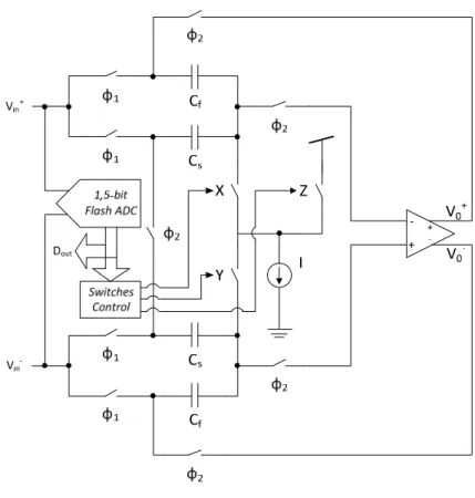
The proposed 1,5‐bit pipeline stage is represented by the figure 3.1.2. In that figure it’s
represented three structures: the OPAMP, 1,5‐bit Flash ADC and switched capacitor network.
1 1
2
0
50 3 – Implementation of the Traditional Pipeline ADC
The switched capacitor network has a feedback factor associated with the number of capacitors
in the circuit. Since the stage resolution is 1,5‐bit it is only needed two equal capacitors. So the
equation ( 2.2.1.7) without the input parasitic capacitance of the OPAMP will transform into:
2. 1 2
(3.1.2)
This feedback factor is going to affect the accuracy requirements needed for the OPAMP, but
also has problems with the thermal noise, which is for capacitors:
2. .
(3.1.3)
Where is the Boltzman constant which is:
1,38 10
(3.1.4)
And T is the absolute temperatures where it is assumed the circuit will work. The normal
temperature is 28ºC which is:
273 º 301
(3.1.5)
Since the maximum error allowed is:
2 2 2 0.1953
(3.1.6)
Where 400 .
The capacitor value is determined in order to obtain a thermal noise value bellow the desired
value. In terms of representation for respecting the thermal noise accuracy it’s all the capacitors
3.1 – MDAC 51
Figure 3.1.3 – Plot of capacitor thermal noise for a 10‐bit ADC
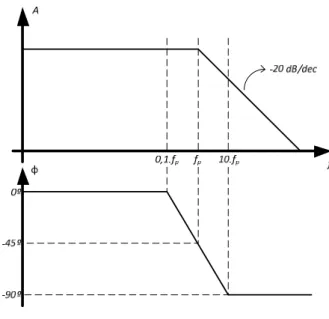
The OPAMP presented in the design is considered a single‐pole OPAMP, with bode diagram like
the one represented in the figure 3.1.4.
Figure 3.1.4 – Bode diagram of the transfer function of a single‐pole OPAMP
0.1 1 10
1 10 4 2 10 4 3 10 4 4 10 4
(pF)
(V)
5 10 4
105 v.n Cap( )
.max
10
52 3 – Implementation of the Traditional Pipeline ADC
The positioning of the pole in the OPAMP will limit the resolution and sampling frequency of the
design where the OPAMP is used. So it is necessary to arrange equations for finding the best
specifications for the OPAMP. This has the following mathematical expression for its open‐loop gain:
1
(3.1.7)
Where is the finite DC gain. Also the closed‐loop gain is:
1 . β 1 .
1 1
1 .
(3.1.8)
Knowing that the input signal is of the following type:
.
(3.1.9)
Where is a unit step function.
Applying the Laplace Transform to the previous equation will result in:
(3.1.10)
The output of the OPAMP is obtained by multiplying the transfer function of the closed‐loop gain
with the input signal. So the output of the closed‐loop gain is:
. 1 . 11
1 .
(3.1.11)
Applying the inverse Laplace Transform to equation (3.1.11):
1 1 . . (3.1.12)
Where:
1 . (3.1.13)
Rewriting the equation (3.1.12):
3.1 – MDAC 53
So in equation (3.1.14) it is possible to see the non‐idealities of the OPAMP present in each of the
pipeline stage, which includes the finite OPAMP gain, finite time‐settling, but doesn’t take into
account the mismatch in the switched capacitor network.
So a mismatch in the capacitors changes the feedback factor equation into:
(3.1.15)
To take the mismatch into account the equation (3.1.14) has to be changed into:
1
1 1 . .
(3.1.16)
Using the zone where Δ , it has the following transfer function:
V Gain. Δ
(3.1.17)
Where of equation (3.1.16) is equal to Δ , so the Gain is:
Gain 1 1 1 . 1 1 .
1
1 11
1 1
. 1 1
1
. 1
1
(3.1.18)
Where .
There are three terms in the previous equation where two of those are caused by a non‐ideal
effect. The first one, 1 , is the term responsible for the voltage gain. The second one is related
with the finite OPAMP gain. The last term with the exponential function is related with the settling
time for a single‐pole OPAMP, with its respective time constant .
If B is the per‐stage resolution the ideal gain per‐stage is given by:
2
(3.1.19)
54 3 – Implementation of the Traditional Pipeline ADC
The gain error term can be achieved by:
Δ
2 1 11
. 1
1
2
1
2 2 1
1 1 . 1 1 (3.1.20)
Simplifying the previous equation and normalizing the error:
Δ 2 1 . Δ
2 . Δ , 2 . 1 . (3.1.21) Where: ∑ , 2 Δ
Δ , ,
(3.1.22)
In order to follow the N‐bit accuracy, the normalized gain error, should be less than , where
N is the full resolution of the pipeline ADC. The reason for this restriction is to prevent missing codes.
[11]
Δ 1
2
(3.1.23)
From previous equations three design requirements can be extracted: the OPAMP DC gain, the
OPAMP bandwidth, the capacitor matching accuracy and thermal noise.
For the OPAMP gain, it’s reasonable that
. « , because it’s the most flexible design
requirement. So:
1 . «
1
2 ⇒
2
2 2 .
3.1 – MDAC 55
If there isn’t no input parasitic capacitance the previous expression reduces to 2 . But
because of process variations, and to make the ADC more reliable, this value needs to be at least two
to three times larger than this theoretical value.
For a regular operation the OPAMP has to have a settling time of half clock period
in which the OPAMP settles with an error of . So:
1
2 ⇔ log
1
2 ⇔ log 2 ⇔
. log 2 .
(3.1.25)
Starting to analyze the capacitor matching the transfer function can be written as:
1 ∑ , . ∑ . ,
(3.1.26)
⇔ 1 Δ ∑ . . ,
(3.1.27)
⇔ 1 Δ 1 . , Δ
(3.1.28)
Where is controlled by the Flash ADC and can have the following value:
1, Δ 4
0, 4 Δ 4
1, Δ 4
(3.1.29)
The Δ is the error related with the switched capacitors circuit. And its value is:
Δ 1 .ΔC,
(3.1.30)
This is one of the major concerns in the design of the pipeline ADC, because this error takes an
immediate action on the output voltage of the pipeline stage. So to take this error in check the
56 3 – Implementation of the Traditional Pipeline ADC
Δ 2 2
(3.1.31)
So:
1
.Δ ,
C 2 ⇔
1
2 .
Δ , C
1
2 ⇒
Δ 1
2 (3.1.32)
3.1.1
–
OPAMP
sharing
Like it was previously mentioned the main concern in this thesis was trying to answer if the new
MDAC approach can mask the high‐frequency bounding wires effects. So in a similar way when the
Foundries are testing the new process they use a ring oscillator to test it, in this thesis the simplest
design was to have a 1,5‐bit per‐stage resolution.
This simplification is not the best when tackling the power dissipation problem because it needs
eight OPAMPs for each of the eight switched capacitor networks. By sharing an OPAMP between two
consecutive stages in the pipeline the power consumption of the Pipeline ADC can be reduce
significantly [16], by reducing the number of necessary OPAMP by half. This implementation is
represented in the figure 3.1.1.1.
in
V V0
ref V
Figure 3.1.1.1 – OPAMP sharing technique
The use of this technique it is only possible because of the temporal way that the switched‐
3.1 – MDAC 57
of a clock cycle, which is during the amplification phase, and it’s doing nothing during the sampling
phase.
Not Shared Shared
Amplificationstage n‐1 of
Amplificationstage n of Amplificationstage n of Figure 3.1.1.2 – OPAMP time division
There are some high‐precision circuits that use the sampling phase to carry offset cancelation
during this phase. Because if a pipeline ADC has interstage offset, this tends to make the ADC non‐
linear.
The non‐linearity on the pipeline ADCs only occurs if there isn’t any redundancy, because if there
is the interstage offset that are less than the correction range will only cause input‐referred ADC
offset [12].
The sharing of OPAMP will be made between the adjacent stages [13] [14] because of those two
stages have theirs switched‐capacitor networks operating at opposite clock phases. Since they are in
opposite clock phases it is possible to share the OPAMP between the two stages.
The decision circuits can also be shared between the two stages [15] but since the decision
circuits used in this thesis need the two clock phases to produce its output and they only produce a
small percentage of dissipated power.
This technique consists in switching the electrical connections of the input and output of the
OPAMP depending of the phases of the two adjacent stages. For example, in the figure 3.1.1.1, the
stage n‐1 is in sampling phase, that means that the OPAMP traditionally is in idle state or offset
sampling mode, but the next stage is in amplification phase and in need of an OPAMP. So instead of
having the OPAMP doing nothing in sampling phase the designer can have it doing its work where is
needed.
The only difference of this technique from the traditional structure is the two additional switches
58 3 – Implementation of the Traditional Pipeline ADC
Figure 3.1.1.3 – Block schematic pipeline stage of the shared OPAMP
This technique introduces two side effects. The first effect is the introducing of series resistance
by the new switches, which in combination with the OPAMP input capacitance will affect the settling
behavior of the stage.
The switch resistance can be reduced if the switches are enlarged but this will also increase the
parasitic capacitances in the switch. This has the potential to increase the offsets due to the charge