José Miguel Gomes Costa
Numerical Simulation of the
Reflow Soldering Process
José Miguel Gomes Costa
Numer ical Simulation of t he R eflo w Solder ing Pr ocess
Master Thesis
Integrated Master in Mechanical Engineering
Work accomplished under orientation of
José Carlos Fernandes Teixeira
Delfim Fernandes Soares
José Ricardo Barros Alves (Bosch Car Multimedia)
José Miguel Gomes Costa
Numerical Simulation of the
Reflow Soldering Process
In first place I would like to thank to all people that help me in a way or another in the development of this thesis.
A special thanks to my mentors, Prof. Doctor José Carlos Fernandes Teixeira, Prof. Doctor Delfim Fernandes Soares and Dr. José Ricardo Barros Alves, for their personal effort in the attribution of this theme and particularly in make possible my internship at Bosch Car Multimedia. Thank you also by the help, orientation, and time dispensed during the entire project.
Thanks to Mr. Nelson Rodrigues for the help with familiarization with the ANSYS Fluent software. Also thank for the advices related to the simulations and for the clarification of some doubts.
I also thank to all people at Bosch Car Multimedia that helped me in this thesis. Especially to Dr. Ricardo Alves that was my mentor during the internship at Bosch, for all dedication, patience and time spent in the work done at Bosch. Thank to Ms. Lais Oliveira and to Mr. Miguel Peixoto for the help in the realization of the Reflow thermal simulation of a real electronic product at Bosch. Also thank to some friends done during the internship, as Vera Vilas Boas, Sofia Mouta, and Roberto Magalhães for all the help, advices and good disposition.
I would like to also thank to my friends and colleagues of internship at Bosch Car Multimedia, Daniel Barros, Andreia Oliveira, and Susana Rodrigues for all the work realized together, for the support, for the motivation, and for the good disposition.
Finally, I address my greatest thank to my parents and brother for all the support demonstrated along my academic journey and by the effort made so I could finish my master's degree.
The work developed in this thesis is inserted in a large project involving the University of Minho and the Bosch Car Multimedia, in which it is intended to create a numerical model capable of simulate the Reflow soldering process. Thus, during this thesis will be given a small contribution to the creation of this model by continuing the work already developed by Costa (2014), student who initiated this project in his master's thesis.
Before starting the development of the simulation model, it is performed a brief description of the electronic products manufacturing process and its composition, such as PCBs, electronic components and solders used. Being even discussed in greater detail the Reflow soldering process. To carry out this simulation model it is used the computational program ANSYS Fluent being analyzed its way of functioning and the main models used during the simulations, as the VOF model (Volume of Fluid) and the Solidification/Melting model.
Regarding the development of the simulation model, the first step passed by the analysis of the work carried out by Costa (2014), which it resulted in detection of a problem in his last model, related to the deformation of solder paste at room temperature. In an attempt to prevent this deformation several variables were analyzed such, as density, viscosity and surface tension of solder paste, as well as the presence of gravity and the Mushy-zone parameter in order to understand their impact on the solder paste deformation at room temperature. Through this analysis, it was found a solution which involves the alteration of Mushy-zone parameter and the use of a surface tension of solder paste function of temperature. With this solution it was possible to create a model for the fusion of solder paste, with the objective to validate the solution found and to analyze the deformation of solder paste. Finally, it developed a simulation model that allows to simulate any Reflow thermal cycle and to analyze the deformation of solder paste during the entire thermal cycle, including its melting and solidification.
In parallel with this project, it was accomplished at Bosch the thermal simulation of the Reflow soldering process of a real product and compared the values obtained with the actual data from the production line.
Keywords
O trabalho desenvolvido nesta tese está inserido num projeto de grande dimensão, envolvendo a Universidade do Minho e a Bosch Car Multimedia, no qual se pretende criar um modelo numérico capaz de simular o processo de soldadura por Reflow. Desta forma, durante esta tese será dado um pequeno contributo para a criação deste modelo, através da continuação do trabalho já desenvolvido pelo Costa (2014), aluno que iniciou este projeto na sua tese de mestrado.
Antes de iniciar o desenvolvimento do modelo de simulação é realizada uma pequena descrição do processo de produção de produtos eletrónicos e da sua composição, como os PCBs, os componentes eletrónicos e das soldas utilizadas. Sendo ainda abordado com maior detalhe o processo de soldadura por Reflow. Para a realização deste modelo de simulação é utilizado o programa computacional ANSYS Fluent, sendo analisada a sua forma de funcionamento e os principais modelos utilizados durante as simulações, como o modelo VOF (Volume of Fluid) e o modelo Solidification/Melting.
Quanto ao desenvolvimento do modelo de simulação, o primeiro passo passou pela análise do trabalho desenvolvido pelo Costa (2014), o que resultou de deteção de um problema no seu último modelo, relacionado com a deformação da pasta de solda à temperatura ambiente. Numa tentativa de impedir esta deformação várias variáveis foram analisadas, tais como densidade, viscosidade e tensão superficial da pasta de solda, bem como a presença da gravidade e o Mushy-zone parameter, por forma a perceber o seu impacto na deformação da pasta de solda à temperatura ambiente. Através desta análise foi encontrada uma solução que passa pela alteração do Mushy-zone parameter e pela utilização de uma tensão superficial da pasta de solda função da temperatura. Com esta solução foi possível criar um modelo para a fusão da pasta de solda com o objetivo de validar a solução encontrada e analisar a deformação da pasta de solda. Por último, é desenvolvido um modelo de simulação que permite simular qualquer ciclo térmico de Reflow e analisar a deformação da pasta de solda durante todo esse ciclo térmico, incluindo a sua fusão e solidificação.
Paralelamente a este projeto foi realizada na Bosch a simulação térmica do processo de Reflow de um produto real e a comparação os valores obtidos com os dados reais da linha de produção.
Palavras-Chave
Acknowledgments ... iii
Abstract ... v
Resumo ... vii
Index of Figures ... xiii
Index of Tables ... xvii
List of Symbols ... xix
List of Abbreviations, Initials and Acronyms ... xxi
Chapter 1 Introduction ... 1
1.1 Motivation ... 1
1.2 Objectives of the Work ... 2
1.3 Thesis Structure ... 3
Chapter 2 Physical Problem Definition ... 5
2.1 State of the Arte ... 5
2.2 Definition and Fabrication of PCBAs ... 8
2.2.1 Reflow Line ... 8
2.2.2 Radial Line ... 9
2.2.3 Wave Line ... 10
2.3 PCBs ... 11
2.3.1 Immersion Tin ... 12
2.3.2 ENIG (Electroless Nichel/Immersion Gold) ... 13
2.3.3 OSP (Organic Solderability Preservative) ... 13
2.3.4 HASL (Hot Air Solder Leveling) ... 14
2.4 Solder ... 14
2.4.1 Solder Types ... 15
2.5 Electronic Components ... 16
2.5.1 THT (Through Hole Technology) ... 16
2.5.3 Components Metallization ... 18
2.6 Reflow Soldering Process ... 19
Chapter 3 Numerical Models and Methodology ... 23
3.1 Multiphase Flows ... 23
3.1.1 Approaches to Multiphase Modeling ... 24
3.1.2 Volume of Fluid (VOF) Model ... 25
3.2 Solidification/Melting Model ... 30
3.3 Finite Volume ... 33
3.4 Finite Volume Notation ... 33
3.5 6SigmaET Overview ... 35
3.6 Experimental Work Procedure ... 36
Chapter 4 Test Cases ... 37
4.1 Reference Model ... 38
4.2 Reference Model Test and Problem Found ... 41
4.3 Influence of some Variables in the Solder Paste Deformation ... 43
4.4 Influence of Mushy-zone Parameter in the Solder Paste Deformation ... 44
4.5 Solution and Validation ... 45
4.6 Thermal Cycle ... 46
4.7 Study Case at Bosch ... 47
Chapter 5 Results and Discussion ... 53
5.1 Reference Model ... 54
5.2 Reference Model Test and Problem Found ... 56
5.3 Influence of some Variables in the Solder Paste Deformation ... 59
5.3.1 Problem Correction First Attempt ... 62
5.4 Influence of Mushy-zone Parameter in the Solder Paste Deformation ... 64
5.4.1 Problem Correction Second Attempt ... 65
5.5 Solution and Validation ... 66
Chapter 6 Conclusions and Future Work ... 83
6.1 Conclusions ... 83
6.2 Future Work ... 85
Figure 2.1 - Reflow line (Adapted from [16]). ... 9
Figure 2.2 - Radial line (Adapted from [16]). ... 9
Figure 2.3 - SMD components fixed with an adhesive on the face B of the PCB. ... 10
Figure 2.4 - Wave line (Adapted from [16]). ... 11
Figure 2.5 - Constitution of a multilayer PCB (Adapted from [20]). ... 12
Figure 2.6 – THT (Through Hole Technology). ... 17
Figure 2.7 - SMT (Surface Mount Technology). ... 18
Figure 2.8 - Different layers of components metallization. ... 18
Figure 2.9 - Operation principle of a Reflow oven [34]. ... 20
Figure 2.10 – Typical Reflow thermal cycle for lead-free solder pastes (Adapted from [36]). ... 20
Figure 3.1 - Notation for simulation domain division (Adapted from [46])... 34
Figure 3.2 - Notation of the nodes and control volume faces (Adapted from [46]). ... 34
Figure 4.1 – Reference model simulation domain. ... 39
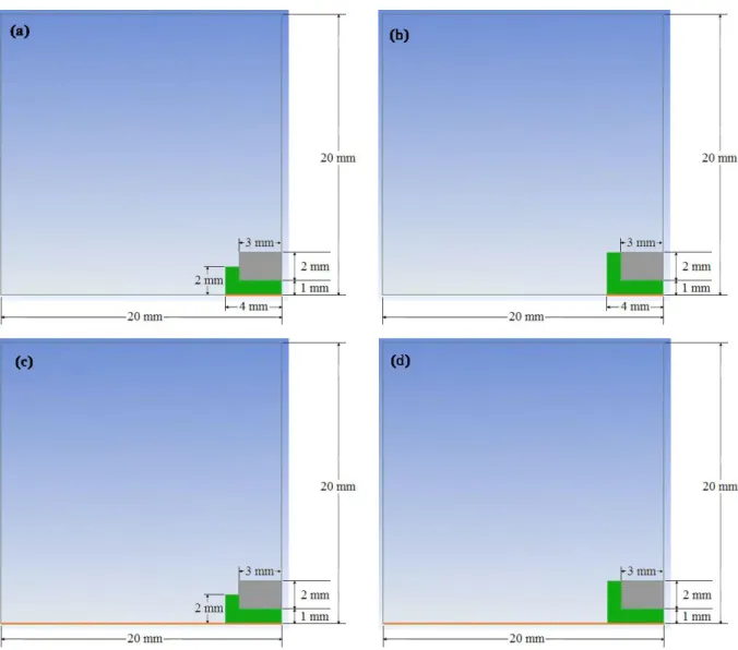
Figure 4.2 – Simulation domain with a small copper pad and a normal quantity of solder paste (a) and with a high quantity of solder paste (b). Simulation domain with a big copper pad and a normal quantity of solder paste (c) and with a high quantity of solder paste (d). ... 42
Figure 4.3 – Surface tension variation function of temperature. ... 45
Figure 4.4 – Simplified Reflow thermal cycle, used in the simulation. ... 46
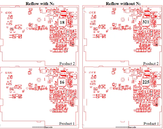
Figure 4.5 – Average of AOI pseudo-errors per component, in the Reflow soldering process with and without N2. ... 48
Figure 4.6 – Product to be simulated with the 6SigmaET. ... 49
Figure 4.7 – Simulation domain of the program 6SigmaET. ... 50
Figure 4.8 – Thermal cycle of the Reflow oven used to produce the product in analysis and perform the simulation. ... 50
Figure 4.9 – Real product with thermocouples installed. ... 51
Figure 4.10 – Thermal cycle of the Reflow oven used to test the product in analysis. ... 52
Figure 5.1 – Initial state of simulation. ... 54
Figure 5.2 – Liquid solder paste deformation in the presence of a component (Adapted from [34]). ... 55
Figure 5.3 – Temperature variation in the simulation domain (Adapted from [34]). ... 56
Figure 5.4 – Solder paste deformation at room temperature. ... 56
Figure 5.5 – Solder paste deformation with a shorter copper pad. ... 57
Figure 5.6 - Solder paste deformation with a shorter copper pad and with more solder paste. .. 58
Figure 5.7 - Solder paste deformation with a bigger copper pad. ... 58
Figure 5.8 – Solder paste deformation with a bigger copper pad and with more solder paste. .. 59
Figure 5.9 – Density increase of 10 times (a) and 100 times (b), relatively to the reference model. ... 60
Figure 5.10 - Viscosity increase of 10 times (a) and 100 times (b), relatively to the reference model. ... 60
Figure 5.11 – Surface tension increase of 10 times (a) and 100 times (b), relatively to the reference model. ... 61
Figure 5.12 – Gravity absence. ... 62
Figure 5.13 – Surface tension equal to 0 N/m and contact angles equal to 90˚. ... 63
Figure 5.14 - Surface tension equal to 0 N/m, contact angles equal to 90˚ and gravity absence. ... 63
Figure 5.15 - Mushy-zone parameter of 107 (a) and 108 (b). ... 64
Figure 5.16 – Mushy-zone parameter of 107 (a) and 108 (b), and surface tension of 0 N/m. .... 65
Figure 5.17 – Solder paste deformation and temperature after 0.5 s of simulation. ... 66
Figure 5.18 – Solder paste deformation and temperature after 0.76 s of simulation. ... 67
Figure 5.19 - Solder paste deformation and temperature after 1.2 s of simulation. ... 68
Figure 5.20 – Simplified Reflow thermal cycle, initial state. ... 68
Figure 5.21 - Simplified Reflow thermal cycle, at 1.4 s of simulation. ... 69
Figure 5.22 - Simplified Reflow thermal cycle, at 1.5 s of simulation. ... 69
Figure 5.23 - Simplified Reflow thermal cycle, at 1.73 s of simulation. ... 70
Figure 5.24 - Simplified Reflow thermal cycle, at 2.16 s of simulation. ... 71
Figure 5.25 - Simplified Reflow thermal cycle, at 3 s of simulation. ... 72
Figure 5.26 – Product 5106, Reflow thermal simulation, after 100 s of simulation. ... 73
Figure 5.27 - Product 5106, Reflow thermal simulation, after 200 s of simulation. ... 73
Figure 5.31 – Temperature difference between the QFP components (C2 - C1). ... 76 Figure 5.32 – Real Reflow thermal cycle of the QFP components and solder joints. ... 78 Figure 5.33 – Real temperature difference between the QFP components and solder joints. ... 78
Figure 5.34 – Sectional cuts of the QFP component’s pins, in a product produced with N2 in the
Reflow soldering process (a), and in a product produced without N2 in the Reflow soldering
Table 2.1 – Solder alloy classification in function of particle size (Adapted from [14]). ... 16 Table 2.2 - Constitutions most used for components metallization (Adapted from [14]). ... 19 Table 4.1 – Material properties (Adapted from [34]). ... 39
Symbol Designation Unities
Constant of mushy-zone
Specific heat at constant pressure [J/(kg.K)]
Node at right of the point P
Total energy [J]
Point two nodes to the right of P
Energy of the phase qth [J]
⃗ Force vector [N] ⃗ Gravitational acceleration [m/s2] Enthalpy [J/kg] Sensible enthalpy [J/kg] Reference enthalpy [J/kg] Thermal conductivity [W/(m.K)]
Effective thermal conductivity [W/(m.K)]
Latent heat of the material [J/kg]
̇ Mass transferred from the phase p to the phase q [kg/s]
̇ Mass transferred from the phase q to the phase p [kg/s]
Node at top of the point P
Previous time-step
Current time-step
Central node
Pressure [Pa]
Phase qth
Node at bottom of the point P
Source term
Source term [J]
Source term
Temperature of Liquidus [K]
Reference temperature [K]
Temperature of Solidus [K]
Velocity magnitude [m/s]
Volume fraction through the face, based in normal velocity
Cell volume [m3]
⃗ Overall velocity vector [m/s]
⃗ Pull velocity [m/s]
Node at left of the point P
Point two nodes to the left of P
Volume fraction of the phase qth
Volume fraction value in the face of the phase qth
Volume liquid fraction
Latent heat content [J/kg]
Time change [s]
Volume control length [m]
Volume control height [m]
Surface tension [N/m]
Emissivity
Viscosity [kg/(m.s)]
Density [kg/m3]
Abbreviations, Initials and Acronyms
Designation
AOI Automatic Optical Inspection
BGA Ball Grid Array
CFD Computational Fluid Dynamics
CICSAM Compressive Interface Capturing Scheme for Arbitrary Meshes
CM Car Multimedia
ENIG Electroless Nichel/Immersion Gold
Face B Bottom side of the PCB
FVM Finite Volume Method
GUI Graphical User Interface
HASL Hot Air Solder Leveling
HRIC High Resolution Interface Capturing
OSP Organic Solderability Preservative
PCB Printed Circuit Board
PCBA Printed Circuit Board Assembly
QFP Quad Flat Package
QUICK Quadratic Upstream Interpolation for Convective Kinematics
SAC Sn-Ag-Cu
SMD Surface Mount Device
SMT Surface Mount Technology
SPI Solder Paste Inspection
TAL Time Above Liquidus
TH Through-hole
THT Through-hole Technology
UDF User Defined Function
Chapter 1
Introduction
1.1 Motivation
The electronic products are present in our lives all days, even without we realize. They are present in all electronic devices that we use like the computer, the cell phone, the domestic machines, and so on.
Due this fast increase of electronic devices in our lives, the electronic industry is today a business sector with a high growth and very competitive. The constant technological development is other fact that requires a constant innovation and optimization of products and fabrication processes used by these corporations.
Electronic products are known in the electronic industry as PCBAs (Printed Circuit Boards Assembly). These are constituted essentially by three parts, as the PCBs, the electronic components, and the solder. The PCBs (Printed Circuit Boards) are the structural support for the components and at same time they provide the electrical connection between them. The solder is used to connect permanently the components to the PCB and this way establishes an electrical connection between both. The soldering processes most used in the industry are the Reflow and the Wave soldering processes.
In the recent past, the solder paste most used was the alloy Sn-Pb. However, this alloy has in its constitution lead, which was prohibited by specific legislation [1], due its harmful effects for the environment and for the human health.
Chapter 1 - Introduction Numerical Simulation of the Reflow Soldering Process
The prohibition of use lead based solder alloys led the industry to use other solder alloys, which forced the introduction of changes in the production processes, due to its inferior properties. The higher melting point of the new solder alloys is clearly an example of a property of solder paste that decreases the production process window. The soldering temperatures are now higher, which means that the components are closer to their temperature limits and that the soldering process is longer than in the past. All this combined with the increased complexity of PCBAs, which have more and more components, due the increase of its functions coupled with its miniaturization, results is a higher risk of occurring production defects and decrease of products reliability.
To avoid these problems it is now more important than never, the correct layout of components in the PCB, and the prediction of temperatures in the product during the soldering process, before its real production, in order to avoid the problems referred. It is in this point where a new area of study has been growing in the industry, with the objective of simulate the soldering process.
The numerical simulation of the electronic products soldering process, although it is something relatively recent, has already showed great potential to provide in a precise, simple, fast and economical way, the thermal profile of a product during the soldering process. With the simulations results, it is then possible to predict the temperature of each component, the temperature differences in the product and its hottest and coolest points, allowing the redesign of the product to avoid problems during the production.
1.2 Objectives of the Work
With the objective of understanding the different variables that may influence the Reflow soldering process and predict what happens during this process, there are several computational programs available in the market to simulate this soldering process. However, most of them, only do the thermal simulation of the PCB and components and do not allow for the simulation of solder paste and its change of physical phase.
The simulation of solder paste is now the next step in the simulation of Reflow soldering process, since it will allow to predict the solder paste phase, deformation and wetting, during the entire process of soldering. This simulation will thus help in the prediction of soldering errors, such as bridging, in the correct definition of the copper pad dimension and form, as well as in the correct definition of the solder
paste amount that need to be printed in the copper pad. In this way, the simulation of solder paste will allow a higher control level of the soldering process and avoid errors in the production.
The objectives of this work are specifically the following:
Study the deformation of solder paste during its melting, in the presence of a
component.
Study the effect of the copper pad dimension and of the solder paste amount in the
deformation of solder paste, in the presence of a component.
Analysis and definition of variables that have influence in the deformation of solder paste.
Creation of a Reflow thermal cycle simulation model.
Analysis the deformation of solder paste during a simplified Reflow thermal cycle,
specifically in its melting and solidification, in the presence of a component.
Identification the reasons for the difference in the Reflow AOI pseudo-errors found
between two equal components placed in equal products of the same nutzen. 1.3 Thesis Structure
In chapter 2, the fabrication process of a PCBA is analyzed and defined. It is even specified the different types of PCBs, solders, and electronic components normally used in the industry. At the end of the chapter the Reflow soldering process is presented and analyzed with more detail.
Chapter 3 explores the ANSYS Fluent, specifically the discretization model of finite volumes, and the solver models. Two other important models used by ANSYS Fluent are even defined, since they are used in the simulations present in this work: the volume of fluid (VOF) and the Solidification/Melting model.
In chapter 4, the study cases are presented. It is also explained the reasons for its selection, the objectives, the methodology, and the expected results. The results of all cases of study are presented in chapter 5, where they are also analyzed along with the principal conclusions extracted from them.
In chapter 6, the main conclusions this thesis are finally presented and suggested some future work.
Chapter 2
Physical Problem Definition
The present chapter presents the state of the arte related with the simulation of the Reflow soldering process and the basics about the production of Printed Circuit Board Assembly (PCBA) and all the necessary components to produce it.
First, an analysis to the bibliography showing the studies carried out on the simulation of the Reflow soldering process is presented. Second, the production process and constitution of the lines which may be necessary to manufacture a PCBA era presented, as well as the PCBs, the solder, and the electronic components, which may compose the PCBA. Finally, the process of soldering by Reflow is presented in a more extensive way, since this will be used as a reference to do the numerical model. 2.1 State of the Arte
With the objective of upgrading the components layout in the PCBAs, it is currently increasingly the use of CFD software that they allow to predict the temperatures of the PCB and electronic components during its pass by the Reflow oven. In this way, it is possible to reduce temperature differences in the PCB that may cause its distortion or hot points that may cause damages in the electronic components, before the production. However, the numerical simulation of the Reflow soldering process is even a recent technology that it needs to be improved.
Lau, Abdullah and Ani [2] simulated the Reflow soldering process using two software (Multi-physics Code Coupling Interface), where the ANSYS Fluent 6.3.26 is used to simulate the Reflow oven
Chapter 2 – Physical Problem Definition Numerical Simulation of the Reflow Soldering Process
by forced convection and the ABAQUS 6.9 is used to simulate the thermal profile of the PCB and electronic components, with the objective of to observe the thermal answer of the PCB during the pre-heating phase of Reflow.
In this study, five PCBs were used with different levels of complexity (changing the number of components in the PCB) with the objective of identify the differences in the thermal profile of the products. Through the CFD software (ANSYS Fluent 6.3.26) was simulated the flow of hot air inside the oven and it was obtained the heat transfer coefficient along the PCB. The heat transfer coefficient is used than in the finite differences software (ABAQUS 6.9) with the objective of determine the temperature of the PCB along the time.
With this study, it was concluded that the temperature of the PCB decreases with its increase of complexity. It was even possible to conclude that the decrease of temperature happens in two places, around the components, due the difference the heights between the components and the PCB, and between the components, where the air flow is interrupted resulting in a decrease of its velocity and as consequence in a decrease of heat transferred by forced convection. Finally, it was concluded that the increase of complexity of the PCBs also increases the difference of temperature between the hottest component and the coldest solder joint on the PCB.
However, it is possible to change the velocity of the Reflow line in order to minimize the difference of temperature in the PCB. Lau, Abdullah and Ani [2] verified that the velocity decrease of 35 % results in a decrease of the highest temperature difference in the PCB of 2.5 ˚C.
Balázs and István [3] performed a study to understand the air flow inside the Reflow oven. In this study was concluded that there are two zones of laminar flow in the direction of the Reflow oven ends. This it results in a big variation of the heat transfer coefficient in this direction, which may cause problems in the solder joint quality.
One of the main objectives in the numerical simulation of the Reflow soldering process it is the simulation of the solder paste geometry. The Surface Evolver software, developed by Brakke [4], it has been used to simulate the solder paste geometry and it achieved good results. However, this software has the limitation of not simulate cases where the solder paste flows out of the copper pad [5].
In order to overtake this limitation and to take into account the solder mask, it was developed an algorithm by Ya-Yun, Hung-Ju, Jer-Haur and Weng-Sing [6] based in fluid dynamics. With this new model it was possible to achieve all the results of the Surface Evolver software and correct its limitations, and also to analyze the wetting and thickness of solder paste.
Hao, Mattila and Kivilahti [7] used two thermal models, one for the components and other for the solder joints, with the objective of to simulate the solidification of lead-free solder paste, in the presence of a component. The heat transfer coefficient used it was obtained in a previous study [8]. The results for the components model show that the components cool faster than the PCB, and the solder joints model shows that the difference of temperature has no meaning until its solidification.
In order to simplify the simulation of the Reflow soldering process, Whalley [9] instead simulating the entire Reflow oven to obtain the heat transfer coefficients, sensors were placed in a PCB in order to obtain these values directly from the Reflow oven. The PCB was simplified also using a 2D model. As consequence, it is considered that there is not difference of temperature between the components and the PCB area below the components. This assumption it has into account the results achieved by Sarvar and Conway [10] however, it cannot be used in problems with high thermal mass components and where the connection to the PCB do not allow a good conduction of heat. With the model presented by Whalley [9] it was possible to achieve accurate results even with all simplifications, which it allowed to reduce the simulation time.
Srivalli, Abdullah and Khor [11] investigated the effect of different cooling periods in the Reflow soldering process of a BGA IC package. The domain of a lead-free Reflow oven was built in GAMBIT 2.3.16 and the model was exported to Fluent 6.3.26 for further parametric study. Simulation results were validated by experimental data according to the American Society of Mechanical Engineers standard for computational fluid dynamics and heat transfer. The simulations results show that a very
high radiation heat flux (122.760 W/m2) in a short cooling duration result in unmelted solder powders,
which it has a consequence of poor wetting. On the other hand, a reduced heat flux (9.262 W/m2)
affects the mechanical properties of solder balls with its continued cooling. As a conclusion the results show that 111 s was the optimum cooling period to avoid soldering defects.
Costa, Soares, S. Teixeira, Cerqueira, Macedo, Rodrigues, Ribas and J. Teixeira [12] modeled two study cases in ANSYS Fluent. In the first case is analyzed the melting process and the dropping behavior of different materials in a presence of a thermal source. The model is validated using a study case found in the literature and using water as the melting material due its well-known behavior. Finally, tin and SAC 405 were used as melting materials and some variables as surface tension and latent heat of fusion were analyzed also. In the second study case is analyzed the deformation of solder paste (SAC 405) during its melting in a presence of a component and of a copper pad on top of a PCB. The heat source is the copper pad that it has a constant temperature.
Chapter 2 – Physical Problem Definition Numerical Simulation of the Reflow Soldering Process
2.2 Definition and Fabrication of PCBAs
As the name suggests, the PCBA is a product formed by the PCB, the electronic components and the soldering process that attaches the components to the PCB.
In this way, to produce a PCBA it is necessary first produce the different parts that are necessary for assembly the PCBA, know the product, and the required fabrication processes, because different products with different electronic components require different soldering processes.
Normally the companies that produce the PCBA, like the Bosch Car Multimedia, buy all the necessary components and only do the assembly of the electronic components in the PCB and then the soldering process. This assembly process can be more complex than it may seems at first sight. Depending the complexity of the products the fabrication process may need to pass by three lines (the Reflow line, the radial line, and the Wave line) [13].
In the following sections it is explained in a simple way the different steps needed to produce a PCBA in the different lines.
2.2.1 Reflow Line
In a typical Reflow line, like that at Bosch Car Multimedia as depicted in figure 2.1, PCBs are loaded on the line and marked with an individual barcode by laser. After, the solder paste is printed above the pads and it is inspected, to confirm that is correctly printed in all pads and in the right quantities. The next step is the insertion of SMD components in the correct position of PCB. Note that, in this line only SMD components are inserted. The product is subsequently mounted, and ready for the soldering process that occurs in a Reflow oven, where the solder paste melts and solidifies becoming a strong connection between the SMD components and the PCB. When the products leave the Reflow oven they are unloaded in a special container that can load several products, and unload for the AOI (Automatic Optical Inspection) one PCB each time, only when the operator in the visual inspection removes a PCB of the line.
The AOI is the final automatic inspection done in this line, and the objective is to inspect the solder and the SMD components to confirm or not the quality of the product. The operator at the end of the line sees the results of the AOI, if the AIO do not detect any defect the product is considered good. However, if the AOI detects only pseudo-errors, the operator needs to check visually if these pseudo-errors are real errors, occurred in the soldering process or in the insertion of the SMD
components, or if these pseudo-errors in reality do not represent any real error. In the first case the product must be rejected and in the second one the product is considered good. When the AOI detects an error the product must be rejected. After the final inspection, it is the operator who takes manually the products out the line and places them in containers [14] [15].
Figure 2.1 - Reflow line (Adapted from [16]).
At Bosch Car Multimedia a product can have a maximum of three soldering processes, taking into account the Reflow and Wave soldering processes. In this way, an ordinary product can have a single Reflow soldering process, or two Reflow soldering processes, or one Reflow and one Wave soldering processes, or two Reflow and one Wave soldering processes [14].
The products that have only a single reflow have SMD components in only one side of the PCB. However, when necessary do two Reflow soldering processes, the PCB needs two passes in the Reflow line. In the first pass are inserted SMD components in one side of the PCB. Then the PCB is placed upside down and the second pass begins at the Reflow line to insert SMD components in the other side of the PCB [14].
2.2.2 Radial Line
The products that leave the Reflow line may need to come to the radial line, figure 2.2, to do the automatic insertion of radial components and, if necessary, the placement of SMD components on the face B of the PCB [14].
Chapter 2 – Physical Problem Definition Numerical Simulation of the Reflow Soldering Process
Once the products coming from the Reflow process enter the radial line from the loader, the components are inserted, and the length excess of metallic pins of the components is cut. Subsequently, the PCBs are rotated and pass by a process of vibration and suction to clean the product, of metal filings that may be in the PCB that result of cutting metallic pins. In the case of the product having SMD components in the face B to be soldered by Wave soldering process, it is necessary to apply an adhesive to the PCB, between the pads where the component sits, and then place the SMD components above the adhesive, as presented in figure 2.3 [14].
Figure 2.3 - SMD components fixed with an adhesive on the face B of the PCB.
In the next step the adhesive is cured in an o en at C, hardens and holds the component to the PCB. This process is necessary because during the Wave soldering process the components are upside down, so, an adhesive is necessary to hold the components in place during the process. After the curing of adhesive, the products are unloaded in a container, and at the end of the line is done the AOI, where the operator puts the product in the machine, evaluates the results, and removes the product out the line [14]. All products that need Radial components, or SMD components in its face B, arrive to this line to be soldered by Wave soldering process [14].
2.2.3 Wave Line
The Wave line is the last line in the process of fabrication the one PCBA. The products coming from the Reflow line or Radial line enter this line from the loader, through an operator who picks the product and puts them into the line. The next step is the manual insertion of TH components, if necessary. Then the products pass in the AOI to check if the product contains all the components in the right position. When the products arrive to the Wave oven, three distinct processes occur: a) the flux is
applied to the surface of the product that needs to be soldered; b) this surface is pre-heated and c) the Wave soldering occurs.
After the Wave oven, the products are cooled by fans, to allow the operator handle them out the line, and place them in the AOI. In the AOI the operator verifies if the product is free of soldering defects or bad component alignment. If the product presents some defect, and depending on the defect, this maybe has reparation, which is performed by an operator. However, if the product is free of defects, the operator removes it from the line, and the product is completed [14] [17]. The Wave line is presented in the figure 2.4.
Figure 2.4 - Wave line (Adapted from [16]).
2.3 PCBs
The PCBs have in the PCBAs two main functions: a) provide to the electronic components the structural resistance to maintain them in the right position, and b) the electrical connections between the different electronic components in the PCB.
The PCBs are produced from FR-4 as a base material, which is a substrate of fiberglass impregnated in epoxy resin. In addition to the base material the PCBs have in your constitution printed electrical copper circuits (tracks) that provide the necessary electrical connections. Depending of complexity of the PCBs, these copper circuits may be printed only in one face, in both faces, or in multilayer. In the last case, presented in figure 2.5, in addition to the printed copper circuits in the faces of PCBs, these are also printed inside of the PCB. This method is used when the density of electrical connections is high for only two superficial layers in the faces of the PCBs.
The connection between the printed copper circuits and the electronic components is done by copper pads. To connect different copper layers it is used metalized copper holes (vias) that may pass through the entire thickness of the PCB [18] [19].
Chapter 2 – Physical Problem Definition Numerical Simulation of the Reflow Soldering Process
Figure 2.5 - Constitution of a multilayer PCB (Adapted from [20]).
After the PCBs production, it is necessary protect the copper with a surface finish. This process is done mainly to avoid the oxidation of the copper pads. However, the surface finish is also used to improve the solderability, and to minimize the copper diffusion during the soldering process.
In the market there are several types of surface finish being the most used the Imersion Tin, the Ni/Au, the OSP, and the HASL. The choice of the surface finish depends of several factors as solderability, cost, and product quality. So, different surface finishes yield different intermetallic compounds, which affects the microstructure and mechanical properties of solder joints. The intermetallic compound created during the soldering process, between the solder and the copper pad, has an extreme importance in the quality and reliability of the solder joints. So, it is important to achieve a good formation of the intermetallic compound, which depends of the solder alloy and the surface finish used [21]. At Bosh Car Multimedia all surface finish need to have a metallization that resists for three soldering processes (Reflow and Wave) as requirement, due its degradation during the soldering processes.
2.3.1 Immersion Tin
The Immersion Tin is a surface finish created from the deposition of tin over the copper on the surface of the PCB, through the immersion of the PCB in liquid tin. The resulting layer of tin has a thickness normally between 0.8 and 1.2 µm, which depends of intermetallic thickness. It is important that the intermetallic do not arrive at the surface, of surface finish, to avoid problems with the solderability and wetting. So, the thickness of surface finish needs to be high enough to have a pure tin layer in its surface. In proper conditions of storage this surface finish protects the copper pads for up to one year. After this period the PCBs need to be analyzed, and if they are still in good condition the
expiration date is extended. This method is the same for every surface finish at Bosch Car Multimedia [22].
2.3.2 ENIG (Electroless Nichel/Immersion Gold)
The Ni/Au surface finish it is in reality two surface finish layers, first the nickel is deposited over the copper pads and after the gold is deposited over the nickel.
In this process the PCB is submersed in a nickel solution, and the deposition process occurs with the help of a reducing agent and without using an electrical current. After the nickel deposition, the PCB is immersed again, now in a solution of gold, where the gold is deposited over the nickel. The thickness of the nickel layer it is comprehended between 3 and 6 µm, and the thickness of the layer of gold between 0.05 and 0.1 µm. The use of the layer of gold it has the principal objective of to protect the nickel from oxidation. During the soldering process the gold layer is dissolved in the solder, exposing the nickel layer that will promote connection with the solder. This surface finish presents normally the best results of all surfaces in terms of soldering quality. Due to the good anti-oxidation protection that it is provided by the gold, resulting in a good solder paste wetting. And due to the presence of nickel that it stops the diffusion of copper. However, the quality increase provided by this surface finish it has a price, since this surface finish is the most expensive [22].
2.3.3 OSP (Organic Solderability Preservative)
The OSP is an organic surface finish with 0.2 to 0.5 µm of thickness that it prevents the oxidation of the PCB copper pads.
Since the OSP is not a solderable surface finish, the copper needs to have an excellent solderability, because it is this surface that will determine the wetting and spreading of molten solder during the soldering process.
The OSP layer is dissipated durin the solderin process at hi h temperatures to C) exposing the copper pads to the flux and environment. With the temperature increase, the solder starts to melt and to wet the copper pads on the PCB. The principal disadvantage of the OSP surface finish is the difficulty in providing a good protection to the copper pads in multiple soldering processes. Since the OSP layer is degraded continuously in each thermal cycle, the last pads to being soldered, after one
Chapter 2 – Physical Problem Definition Numerical Simulation of the Reflow Soldering Process
or two soldering processes, will have a high probability of being oxidized due the degradation of all OSP layer. This it is currently one of the challenges for the PCBs manufacturers with OSP surface finish.
The use of an atmosphere of N2 during the soldering process it is in this surface finish particularly
important, since this atmosphere prevents the copper pads oxidation when the OSP surface is degraded.
The main advantage of OSP surface finish it is the low cost. This it is also suitable for fine-pitch products, when compared with the HASL, due the more uniform layer of OSP that will not interfere with the placement of the fine-pitch components [22] [23].
2.3.4 HASL (Hot Air Solder Leveling)
The HASL surface finish it is accomplished by immersing the PCB into molten solder. The solder alloy used may be a Sn-Pb or a lead-free alloy, depending of required product.
The thickness and texture of the HASL layer, which depends of the surface tension of molten solder, can vary from 2 to 20 µm or more.
HASL advantages can be enumerated as excellent solderability, since the HASL layer it is normally produced using the same alloy that will be used in the soldering process, and as good oxidation protection that it is provided to copper pads by the HASL layer. However, this technology has also some disadvantages, such as the loss of copper due the formation of an intermetallic layer between the copper pad and the HASL layer. Other important disadvantage, it is the not flat HASL layer, making assembling fine-pitch technology difficult or impossible [22].
2.4 Solder
In respect to solders used in electronic industry, it is possible to divide them in two groups, the Sn-Pb and the lead-free solder alloys.
The solder alloys with lead were in the past very often used by the electronic industry, due to their superior properties such as low meltin point C), superior manufacturability and process compatibility. However, the Pb as a toxic substance it was prohibited in the production of electronic components, by specific legislation [1]. This fact created a big change in the electronic industry, and the appearance of a high number of new lead-free solder alloys as substitutes of Sn-Pb alloys [24].
The first studied alloys were binary eutectic alloys of Sn and other elements, including Sn-Ag, Sn-Cu, Sn-Sb, Sn-Zn, Sn-In and Sn-Bi. The Sn-Cu alloy was implemented in the production of low cost products by Nortel [25] and it was achieved good results. The reasons for their choice were the cost and availability in comparison with Sn-Ag alloy. However, Sn-Cu presents inferior mechanical properties and wettability than Sn-Ag alloys [26].
However, the remaining binary alloys have a higher melting point than Sn-Pb, including Sn-Ag. To reduce the melting point, ternary alloys are desirable. Ternary alloys of copper with Sn-Ag were tested in BGA packages and the results obtained present superior performance than Sn-Pb alloys. Quaternary alloys were also tested, where the Sn3.5Ag1Zn0.5Cu was reported as having good properties by McCormack and Jin in 1994. But, problems may be found in the production with this type of alloys, because the difficulties of reproducibility in the composition, result of quaternary alloys complexity [27].
Due the reasons presented above and due the good wetting, resistance to fatigue and plasticity, comparing to others lead free alloys, the SAC (Sn-Ag-Cu) alloys became the main alternative to Sn-Pb alloys. However, the SAC presents a higher melting point than Sn-Pb, etween and C, and due its composition, different intermetallic compounds may be formed during the soldering process, and this can change the properties of solder joints [24].
2.4.1 Solder Types
In the electronic industry is normal find two types of solders as uniquely solder, and solder paste. At Bosch Car Multimedia is used solder paste (SAC 405 + flux) in the Reflow soldering process, and uniquely solder (SAC 305) in the Wave soldering process [14].
The solder paste is composed by two mixed products, solder particles and flux. The solder particles used in solder paste they are classified in terms of size according to the table 2.1.
In high-temperature soldering processes, the primary purpose of flux it is to prevent oxidation of the materials to be soldered. Flux is inert at room temperature but became a stronger reducer at soldering temperatures, protecting and cleaning the surfaces that will be soldered. The flux is made by solvents, activators, vehicles, and additives. The solvents provide to the solder paste a pasty consistency, which it facilitates processing and deposition of solder paste. In the soldering process, the solvents are evaporated during the preheating. The activators have the function of to remove the oxides of surfaces to be soldered. The vehicles are liquid at soldering temperature, and their functions are actuate as barrier against oxidation, dissolve the reaction products of activators and carry them away
Chapter 2 – Physical Problem Definition Numerical Simulation of the Reflow Soldering Process
from the metal surface. At least, the additives are chemical products that may be added to the flux to change its properties, as corrosion inhibitors and antioxidants [28] [29].
Table 2.1 – Solder alloy classification in function of particle size (Adapted from [14]).
As mentioned above, in the Wave soldering process, it is used uniquely solder in the soldering process, however a flux is used separately of solder and before the soldering process to clean the surfaces to be soldered of any contamination or oxidation.
2.5 Electronic Components
Relatively to the components placed in the PCBs, it is important note that there is one important difference between the components. This difference it is related with the placement technology that can be SMT using SMD components or THT using TH components. In a PCBA may exist uniquely one or both technologies, depending of its complexity [14].
2.5.1 THT (Through Hole Technology)
The through hole technology uses through hole components. These components have pins and they are inserted in holes that pass through the PCB. In this kind of technology, the entire hole exposed surface it is the pad, which will be the connection point between the PCB electric circuit and the component’s pins. The connection between the pads and the pins it is done by the solder, which it is placed in most of cases by Wave soldering process, but sometimes for specific components, can be done by Reflow soldering process. In the case of a component TH soldered by Reflow soldering process it is necessary take into account, during the design of electrical circuit of the PCB, the excess of solder paste which it needs to be printed to fill the holes during the reflow. This may be a problem in
Solder alloy type Particle Size Range (µm)
I 150 - 75 II 75 - 45 III 45 - 25 IV 38 - 20 V 25 - 15 VI 15 - 5
components with a large number of pins or in PCBs with a high density of components. In this cases, may does not exist space enough to print the solder paste needed for fill all holes.
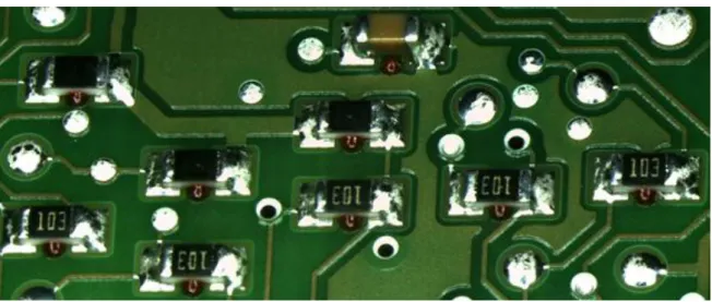
Figure 2.6 presents two through hole components to be soldered by Wave, and three to be soldered by Reflow. In the last ones, it is possible to observe the location specified for the overprint of solder paste near to the pins of the components [30].
Figure 2.6 – THT (Through Hole Technology).
The main disadvantage is that this technology is associated with the use of large components. In this way, the PCB cannot have a high density of components, which it limits the functions or the miniaturization of a PCBA. However, this technology allows for some applications to reduce the production cost, due the lowest cost associated to the machines and process used in the Wave, comparing to the Reflow soldering process [30].
2.5.2 SMT (Surface Mount Technology)
The SMT is a technology more recent than THT and it is totally automated, contrarily to the THT where most of the components are placed by hand.
In the SMT technology, the components are soldered to the pads placed on PCB surface. In this way, it is possible to place components on top and bottom of the PCB.
The use of a fully automated production process is fundamental in this kind of technology, since it uses smaller components and more sensitive than THT. In this process it is also necessary a high precision and control of all production line, to achieve good products.
Chapter 2 – Physical Problem Definition Numerical Simulation of the Reflow Soldering Process
As it is possible to observe in figure 2.7, this technology allows to achieve smaller products or with more functions for the same PCB size, and a production rate higher than THT [30].
Figure 2.7 - SMT (Surface Mount Technology).
2.5.3 Components Metallization
The selection of the components metallization it is an important step on the PCBAs production, because this has the function of protecting the base metal of oxidation and it increases the solderability. At Bosch Car Multimedia, the surfaces or the pins of the components to be soldered are formed essentially by copper, nearly 80%, or formed by Fe-Ni. The last one, it is used principally for components that need to resist to the mechanical stress [14].
The metallization finish layer most used in electronic industry it is the Tin (Sn). This layer may be applied by different techniques and with different thicknesses, depending of its application. In some components or applications in order to avoid defects, as whiskers, it is used a top underlayer of Ni or Cu between the base metal and the finish layer of Sn. In figure 2.8, it is possible to observe the distribution of the layers in a normal component metallization [14] [31].
The finish layer and the top underlayer have different thicknesses, depending on the process of production and the application. It is necessary to take into account the degradation of the metallization during the soldering process, and in this way to produce a metallization that resists to the entire soldering process. Table 2.2 shows the metallizations most used at Bosch Car Multimedia [14].
Table 2.2 - Constitutions most used for components metallization (Adapted from [14]). Metal Lead (Pin) Finish for CM
Base Material Cu-based FeNi
(not recommended) Sn finish layer Galvanic matt min. 2 µm x x x x x x x x min. 7 µm x x x x x x Hot dip plating min. 2 µm x x x x x x Top underlayer Galvanic Ni (min. 0.5 µm) x x ( x ( x x x Galvanic Cu (min. 2 µm) x x x x x x
2.6 Reflow Soldering Process
Reflow is a soldering process that occurs in an oven and where the solder paste is melted and solidified with the objective of attaching the components to the PCBs.
There are different methods to do the Reflow as through forced convection, in-line-conduction, infrared, and vapor phase [32]. However, at Bosch Car Multimedia it is only used the Reflow oven with forced convection, so this will be the focus of this thesis [14].
The forced convection oven, used in the Reflow soldering process, works through movement of
hot gas heated by heat exchangers. This gas is normally N2, which it is a non-oxidant gas, contributing
for a better solderability than air [14]. The gas is in this way the transporter of the heat from the heat exchanger to the PCB. The PCB is heated from top and bottom, and between the inlet, of the oven, and the exit it passes through four phases of heating well defined in terms of temperature and time. Figure 2.9 presents the operation principle of a Reflow oven [33].
Chapter 2 – Physical Problem Definition Numerical Simulation of the Reflow Soldering Process
Figure 2.9 - Operation principle of a Reflow oven [34].
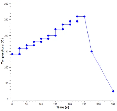
As presented in figure 2.10 the four phases of the Reflow soldering process are: a) the preheating, b) the activation of flux or Soak, c) the Reflow, and d) the cooling [35].
In the preheating phase the PCB and the components are heated at low rate from the room temperature to C [14]. The main objective this phase is to evaporate the solvents of solder paste, and to do this, it is important make sure that the temperature and time of this phase they are the correct to evaporate all solvents. The low rate of heating is also important, because it avoids the thermal shock of the components and PCB, which could damage the components, distort the PCB, or provoke delamination due the different thermal expansion coefficient of the different materials [33].
The second phase named activation of flux or Soak occurs at near constant temperature during a well-defined period. During this phase, as the name suggests, the flux is activated and the oxidation-reduction reaction between the activators and the oxidized surfaces begins. In addition to removing the oxides, the activators also protect the surfaces to be soldered until the beginning of the third phase [14]. To achieve these objectives it is critical to have a perfect control of temperature and time. In fact, higher temperatures increase the oxidation and the activators may last less time that initially predicted, leaving later the solder and pads without protection anti-oxidant. Otherwise, with lower temperatures, the activators may not be entirely activated, not cleaning the surfaces to be soldered properly. The other main objective of this phase is the temperature homogenization around the PCB, this allows that all components are soldered at same time, avoiding hot points and distortions in the PCB and components [33].
The third phase is the Reflow. It is in this phase that the soldering process takes place. The temperature increase almost linearly up to the maximum temperature, etween and C [14], which is defined by taking into account the weakest component in terms of temperature resistance. Subsequently the temperature falls. Higher temperatures may cause damage in the components. However, the maximum temperature has to be high enough to ensure that all points of solder are melted in the PCB during the soldering process, due the temperature gradient around the PCB. Otherwise, low temperatures may not to melt all points of solder. In this way, it is possible understand that the definition of the maximum temperature has a critical importance in all process of Reflow [33].
Other variable extremely important in all soldering process it is the TAL (Time Above Liquidus), normally between 45 and 90 s [14]. This period of time needs to be as shorter as possible to avoid oxidation, but it is necessary to give enough time to melt the solder on all PCB, principally in the cold points. This period it is also important to achieve a good wetting of solder paste and consequently a good solder joint. However, if this period it is too long the intermetallic layer may grow more than desirable and make the solder joint more brittle [33].
Chapter 2 – Physical Problem Definition Numerical Simulation of the Reflow Soldering Process
The last phase is the cooling of the solder joints formed previously. In this phase the rate of cooling needs to be as higher as possible to obtain a solder with a fine granular structure, which it provides better mechanical properties [37]. But as in the preheating phase, it is necessary to be careful with the thermal shock and distortion of the components and PCBs respectively. However, the rate of cooling has influence on the intermetallic layer growth. Slow cooling rates may cause an excessive intermetallic layer growth, and formation of coarse granular structures that weaken the solder joints, resulting in poor stress resistance [33] [38].
Chapter 3
Numerical Models and Methodology
This chapter presents a simple description of the most important models used in ANSYS Fluent, taking into account the objectives of the numerical simulations, an overview of the 6SigmaET software, and a description of the experimental procedure.
First, two models used by ANSYS Fluent are presented, due its importance in the simulations, as the Volume of Fluid (VOF) and the Solidification/Melting Model. Second, the discretization method, the Finite Volume Method, used by ANSYS Fluent to solve the integral systems of equations is described. Third, the thermal simulation software “ Si maET” used in the work de eloped at Bosch ar Multimedia is presented. Finally, the experimental procedure used to validate the 6SigmaET simulations results is described.
3.1 Multiphase Flows
Normally the flows found in nature or in industry they are a mixture of phases. The physical phases of materials are three, gas, liquid and solid, but the concept of phase in multiphase flows it is applied in a more ample way. In multiphase flows one phase can be defined as a class of identified material that it has a particular answer of inertia and it interacts with the flow and with the potential field in which it is immersed. For example, solid particles with different dimensions of the same material can be defined as different phases, because each group of particles with the same dimension going to have a similar dynamic answer to the flow field.
Chapter 3 - Numerical Models and Methodology Numerical Simulation of the Reflow Soldering Process
Multiphase flows regimes can be divided in three categories as: a) flows gas-liquid or liquid-liquid, b) flows gas-solid and c) flows liquid-solid, and flows with three phases. Three-phase flows are combinations of others flow regimes listed above [39].
3.1.1 Approaches to Multiphase Modeling
There are currently two approaches for numerical calculations of multiphase fluids: the Euler-Lagrange approach and the Euler-Euler approach [39].
The Euler-Lagrange Approach
This model is appropriate to modulate spray dryers, combustion of liquid fuel and coal, flows with some particle-laden, but it is inappropriate to modulate flow regimes liquid-liquid, fluidized beds, or any application where the volume fraction of the second phase cannot be neglected [40].
The Euler-Euler Approach
In the Euler-Euler approach, the different phases are processed mathematically as interpenetrating. Once the volume of one phase cannot be occupied by other phases, the concept of volume fraction is introduced. These volume fractions are assumed as a continuous function of space and time and its sum is equal to 1.
In ANSYS Fluent, three different Euler-Euler multiphase models are available, the volume of fluid (VOF) model, the mixture model, and the Eulerian model [39].
The VOF model
The VOF model is a technique of surface-tracking applied to a fixed Eulerian mesh. This model was developed for two or more immiscible fluids where the interface between the fluids has interest. In the VOF model, one unique set of momentum equations is shared by all fluids, and the volume fraction of each fluid in each cell is tracked across the domain.
The VOF model can be applied for stratified flows, free-surface flows, filling, sloshing, the movement of large bubbles in a liquid, the movement of liquid after a dam break, and the steady or transient tracking of any interface liquid-gas [39].
The Mixture Model
The mixture model is developed for two or more phases (fluid or particles). As in Eulerian model, the phases are processed as immiscible. The mixture model solves the mixture momentum equation and it sets relative velocities to define the dispersed phases.
The mixture model is applied to particle-laden flows with low loading, bubbly flows, sedimentation, and cyclone separators. The mixture model can also be used without relative velocities for dispersed phases to model homogeneous multiphase flows [39].
The Eulerian Model
The Eulerian model is the most complex multiphase model of ANSYS Fluent. This model solves a set of n momentum and continuity equations one for each phase. Coupling is obtained by the exchange of pressure and interphase coefficients. The way coupling is done depends of the phase types involved. Granular flows (fluid-solid) are processed in different way that non-granular flows. For granular flows, the necessary properties are obtained by the application of kinetic theory. The change of momentum between the phases depends also of the phase types to be modulated.
The Eulerian model is applied to bubble columns, risers (vertical pipe), particle suspension, and fluidized beds [39].
3.1.2 Volume of Fluid (VOF) Model
Since the VOF model will be used in the present numerical simulations, because it is suitable for steady or transient tracking of any interface liquid-gas, this will be analyzed more carefully.
In addition to the above mentioned, this model has some limitations as [39]:
The VOF model is only available with the pressure-based solver.
The entire domain of simulation has to be filled with a unique phase or a combination of
phases. The VOF model does not allow empty regions where none fluid of any type is present.
Only one phase can be defined as a compressible ideal gas. However, there is no limitation
about the use of compressible liquids when a user defined function is used.
Chapter 3 - Numerical Models and Methodology Numerical Simulation of the Reflow Soldering Process
Steady-State and Transient VOF Calculations
The VOF formulation is based on fact that two or more fluids or phases are not interpenetrating. For each additional phase, the volume fraction of this phase is introduced in some computational cells. In each cell, the volume fraction of all summed phases must be equal to the unity. The variables and properties are shared by the phases and they represent volume-averaged values, since the volume fraction of each phase is known in each local. In this way, the variables and properties are in each cell purely representative of a phase or of a mixture of phases, depending on the values of volume fraction.
In other words, if the fluid, qth has a volume fraction, , in a given cell, then three conditions are
possible [39]:
The cell is empty (of the qth fluid).
The cell is full (of the qth fluid)
0 < < 1 The cell contains an interface between the qth fluid and one or more other fluids.
Based on the local value of , the properties and the appropriate variables for each control
volume will be attributed and calculated, inside the domain. Volume Fraction Equation
The tracking of interface or interfaces between the phases is done solving the continuity equation
for the volume fraction the one or more phases. For the phase qth, the continuity equation has the
following form [39]: [
( ) ( ⃗ ) ∑( ̇ ̇ )
] (1)
where ̇ is the mass transferred from the phase q to the phase p, and ̇ is the mass
transferred from the phase p to the phase q.
As default, the source term is 0, but can be defined as a constant or as a function defined by
the user for the source mass of each phase. The volume fraction equation is not solved for the primary phase. Instead, the volume fraction is calculated based in the following restriction [39]:
∑
(2) The volume fraction equation can be solved through the implicit or explicit time discretization.
The Implicit Scheme
When the implicit scheme is used for time discretization, the following finite-difference interpolation schemes are used by ANSYS Fluent, QUICK, Second Order Upwind and First Order Upwind, and the Modified HRIC, to obtain the face fluxes for all cells, including the cells close to the interface [39].
∑( ) [ ∑( ̇ ̇ )
] (3)
This equation needs the volume fraction values in the current time-step, contrary to the explicit scheme which it needs only the volume fraction values in the previous time-step. In this way, a standard scalar transport equation is solved iteratively for each volume fraction of one secondary phase in each time-step. The implicit scheme can be used to solve stationary and transient problems [39].
The explicit Scheme
In the explicit scheme, the standard ANSYS Fluent finite-difference interpolation schemes are applied to the volume fraction values computed in the previous time-step [39].
∑( ) [∑( ̇ ̇ )
] (4)
where is the current time-step, is the previous time-step, is the volume fraction
value on the face of phase qth, computed from the first- or second- order upwind, QUICK, modified
HRIC, compressive, or CICSAM scheme, is the cell volume, and is the volume flux through the
face, based in normal velocity.
Contrary to implicit scheme, the explicit method does not need to solve the transport equation iteratively for each time-step. When the explicit scheme is used, a time dependent solution must be computed [39], so, with the explicit scheme, only transient problems can be solved.
When an explicit scheme is used for time discretization, the face fluxes can be interpolated using an interface reconstruction or using a finite volume discretization scheme [39].
![Figure 2.5 - Constitution of a multilayer PCB (Adapted from [20]).](https://thumb-eu.123doks.com/thumbv2/123dok_br/17613015.820411/36.892.102.751.104.360/figure-constitution-multilayer-pcb-adapted.webp)
![Table 2.1 – Solder alloy classification in function of particle size (Adapted from [14])](https://thumb-eu.123doks.com/thumbv2/123dok_br/17613015.820411/40.892.78.774.205.449/table-solder-alloy-classification-function-particle-size-adapted.webp)

![Figure 2.10 – Typical Reflow thermal cycle for lead-free solder pastes (Adapted from [36])](https://thumb-eu.123doks.com/thumbv2/123dok_br/17613015.820411/44.892.89.762.684.1086/figure-typical-reflow-thermal-cycle-solder-pastes-adapted.webp)
![Figure 3.1 - Notation for simulation domain division (Adapted from [46]).](https://thumb-eu.123doks.com/thumbv2/123dok_br/17613015.820411/58.892.254.593.102.416/figure-notation-simulation-domain-division-adapted.webp)