Centro de Ciˆencias Exatas e de Tecnologia
Programa de p´os-gradua¸c˜ao em F´ısica
Electronic and Optical Properties of Quasi-2D
Nanostructures and Exfoliated Systems
Diana Mercedes Meneses Gustin
Thesis presented to the Academic Faculty at Universidade Federal de S˜ao Carlos in partial fulfillment of the require-ments for the Doctoral Degree in the Graduation Physics Course
Advisor: Prof. Dr. Victor Lopez Richard
127 f. : 30 cm.
Tese (doutorado)-Universidade Federal de São Carlos, campus São Carlos, São Carlos
Orientador: Victor Lopez Richard
Banca examinadora: Guo-Qiang Hai, Marcos Roberto da Silva Tavares, Marcio Peron Franco de Godoy, Gilmar Eugeio Marques
Bibliografia
1. Método k.p em Sistemas Bidimensionais . 2. Interação Elétron-Fonon. 3. Espalhamento em Duas Dimensões. I. Orientador. II. Universidade Federal de São Carlos. III. Título.
The PhD Thesis presented here is the result of four years of learning in many fields, and certainly it would be different without the contribution and support of many people, friends and relatives. My sincere thanks to all of them who contributed to the success of this work.
First of all, I would like to thank Professor Dr. Victor L´opez Richard for his supervision and for always providing me assistance, guidance and carefully balancing every step of this research. From him I have learned not only about condensed matter physics and nanoscale systems, but also the enthusiasm and curiosity that define someone who really enjoys the work. With him I shaped my notion of ideal scientific work.
This thesis also rely on the valuable contribution of professor Dr. Sergio Ulloa who has been patient in guiding me during my stay at Ohio University. His teachings have profoundly marked my academic vision. I also thank all the students in Professor Sergio’s research group at OU for welcoming me with great cordiality and making the work environment a comfortable space. With special thanks to Nancy Sandler.
I would like to thank my committee members Professor Dr. Marcos Tavares, Hai Guoqiang, Marcio Peron de Godoy and Gilmar Marques for their interest in my work, your dedication is greatly appreciated.
Among many people I had the pleasure of meeting at UFSCar, I thank to all mem-bers (old and new) of the Semiconductor Nanostructures group for the lessons and knowledge transmitted through healthy debates. Special thanks to my friend Lu´ıs A. Cabral, our coffee breaks were not only to pause the work, but necessary to restart the calculations with reloaded strengths.
In particular, I thank my UFABC and UFSCar friends for their unconditional support. Andr´es, Indira, Carlos, Juli´an, Melissa and Marcela always encourage me to do my best
throughout this journey in Brazil. Each one of them in their own unique way is my example. I admire them greatly and I am going to have eternal gratitude and love for them. With all of them my stay, in these unknown lands, has been the most fabulous possible since 2011. Their friendship is more worth than I can express on paper and definitely the world seems better with all of you guys being part of my family.
I thank the solid team for many moments of fun, relax, reflections and hugs. Andrea and Gina have always been here as my close friends. Their companionship maintains my good humor and their encouragement words in countless times have always made me stronger and more confident, with yousolidas I am in continuous growth. Thejaula
has been part os my history, according to each one of your visions, and I am going to be forever grateful for having you girls.
I also would like to thanks my roommate Aurenice, because her life history, faith in the future and convictions have inspired me along this time here, we definitely make a good team.
I am extremely fortunate to count on Max Pinheiro J´unior, who brightened up my days. Tough times become easier with his jokes and his positive outlook when things are not in favor. But words will never do justice for all he gives me in these times, his exceptional dedication has been my constant reminder that I could do better than I think I would; and his charming coherence is always an invitation for sharing a good coffee, a good beer, or a good wine.
With my family I am deeply indebted for their unconditional support at any time and level. Without them this work would be impossible. A big thank to my mother for not just believing, but knowing that I could do this! You are the one who let me finish this cycle, this thesis is for you mom.
Last but not least, I thank the S˜ao Paulo Research Foundation, FAPESP, for financial support through the 2013/24253-5 and 2016/02065-0 projects.
Esta Tese visa estudar, segundo uma abordagem te´orica, as propriedades eletrˆonicas e ´opticas de sistemas quˆanticos semicondutores quasi-2D. Usando como base o modelo
k· p obtivemos um conjunto satisfat´orio de resultados que explicam certos proces-sos ´opticos, descritos a seguir, de sistemas confinados em nanoescala tais como po¸cos quˆanticos ou monocamadas de atomos. A necessidade e a implementa¸cao sistem´atica de novos e mais elevados n´ıveis de aproxima¸cao aos modelos de estrutura eletrˆonica originais tamb´em s˜ao temas amplamente descritos.
Uma das primeiras contribui¸c˜oes deste estudo foi a verifica¸c˜ao da necessidade de uma nova abordagem para descrever as intera¸c˜oes de portador-fonon em po¸cos quˆanticos baseados em GaAs alem da teoria de potencial de deforma¸c˜ao. Assim, a intera¸c˜ao de Fr¨ohlich foi considerada em nosso modelo, revelando a existˆencia de acoplamentos assistidos por fˆonon entre diferentes estados na banda de valˆencia e de condu¸c˜ao, o que por sua vez resultou em mudan¸cas significativas na estrutura eletrˆonica. Os resulta-dos desta abordagem, assim como as simula¸c˜oes e previs˜oes de resultaresulta-dos, permitiram explicar dois efeitos intrigantes: (i) a potencial observa¸c˜ao de magneto-polarons de bu-racos pesados-leves, (ii) a relevˆancia dos estados 2D como intermedi´arios nos processos de relaxa¸c˜ao, auxiliado por fˆonons, a partir de uma estrutura 3D para uma 0D. Outro sistema estudado foi o dissulfeto de molibdˆenio (M oS2) bidimensional, no qual
This thesis is aiming to study, according to various theoretical approaches, the elec-tronic and optical properties of quasi-2D semiconductor quantum systems. Using the
k·p model as a basis, we obtained a satisfactory set of results that explain certain optical processes, described below, of nanoscale confined systems, such as quantum wells or monolayers of atoms. The need and the systematic implementation of new and higher levels of approximation from the original electronic structure models also are themes broadly described here.
One of the first contributions of this study was the verification of the necessity of a new approach to describe the phonon-carrier interactions in GaAs-based quantum wells, beyond the deformation potential theory. Thus, the Fr¨ohlich interaction was considered in our model, revealing the existence of phonon assisted couplings between different states in the valence and conduction band, which resulted in significant changes in the electronic structure. The results of this approach, as well as the simulations and new predictions allowed us to explain two intriguing effects: (i) the potential observation of magneto-polarons of light-heavy holes, (ii) the relevance of 2D states as intermediaries in relaxation processes, assisted by phonons, from a 3D structure to a 0D.
Another system studied was the two-dimensional molybdenum disulphide (MoS2), in
1 Introduction 17
2 Electronic Structure and Phonons Effects in Quantum Wells 23
2.1 k·p Model . . . 24
2.2 Electronic Structure of Quantum Wells . . . 27
2.2.1 Quantum Well Conduction and Valence Band Calculations . . . 31
2.3 Carrier-Phonon Interaction . . . 33
3 Spin-Resolved Photo-Generation Filtering Induced by Phonon 47 3.1 Theoretical Simulation . . . 53
3.2 Magneto Absorption . . . 55
3.3 Spin Decoherence . . . 63
4 Electron Dynamics in 2D Semiconductors Layers 67 4.1 Scattering Theory in Two Dimensions . . . 69
4.2 Scattering Phase Shift . . . 72
4.2.1 Dirac Case . . . 72
4.2.2 Parabolic Approximation: Schr¨odinger Case . . . 76
4.3 Probability Density and Differential Cross Section . . . 80
4.4 Asymptotic Analysis . . . 86
4.4.1 Dirac Formulation . . . 86
4.4.2 Schr¨odinger Formulation . . . 89
5 Conclusions and Final Considerations 93
Appendices
A Matrix Representation of the Luttinger Hamiltonian 99
B Rotation of Luttinger Hamiltonian for Zincblende Crystal 103
C Scattering Systems 105
C.1 Dirac Dynamic . . . 105
C.1.1 Schr¨odinger Dynamics . . . 108
C.2 Asymptotic Analysis . . . 111
C.2.1 Dirac Formulation . . . 111
Introduction
The attractiveness of the nanoscaled physical systems comes from the ability to increase the functionality and performance of the next generation of devices, substituting in this way the classical microelectronincs. Due to the fact that the dimensions of these nanos-tructures are comparable to the de Broglie wavelength of the electron, their electrical, optical and mechanical properties are described by quantum mechanics. Here, we will take advantage of some quantum phenomena in order to described and tuning the carriers behavior in two dimensional systems.
Among a variety of materials used for growing nanostructres, special attention has been directed to the heterostructures formed by semiconductors compounds, even over metal or dielectrics substrates. This remains as an important topic for technology and industry, specially due to the switching capability of diodes, photovoltaic cells, transistors, detectors and thermistors. Typical semiconductors structures are composed of alloys of the IV group elements and/or III-V and II-VI compounds. A prolific use have the GaAs and InAs based structures, particularly during the last few decades [1–4], in part due to the relatively easy fabrication and the capacity to confine electrons and holes when they are combined with other semiconductors, yielding to the emergence of nanostructures such as GaAlAs/GaAs or InGaAs/GaAs.
There are several fabrication techniques employed to obtain semiconductor nanostruc-tures of high quality such as molecular beam epitaxy (MBE), chemical beam epitaxy (CBE) and metal-organic chemical vapor deposition (MOCVD) [5, 6]. The choice for the crystal growth as well as its design is related with the number of directions along
which the carriers could be confined [7]. Structures where carriers are confined in the three spacial directions are called quantum dots [8]. In turn, in quantum wires, the electrons and holes are confined in two spatial directions [9, 10]. While, in quantum wells the charge carriers are confined just in one direction whereas their movement is free along the other two [11, 12].
Another way developed to exploit the quantum phenomena from the size quantiza-tion is inspired in the convenquantiza-tional exfoliaquantiza-tion techniques similar to the ones used for graphene synthesis [13]. By scaling down the transition metal dichalcogenide bulk un-til a monolayer, carriers are restricted to move into a two dimensional lattice. This exfoliation is possible due to the weak bonds between the staked layers. As well as the graphite case, the transition metal dichalcogenides have their layers weakly bound by van der Walls forces allowing to a repetitive cleavage of the bulk until the single-layer form.
This thesis presents a sequence of novel results derived from a systematic investigation of the hybridization states and scattering effects, evidenced on the optical response as well as in the transport and electronic properties of quasi-bi-dimensional (2D) semi-conductor systems such as quantum wells and monolayer systems. The study was developed in collaboration with experimental groups of growth and spectroscopy (GNS-UFSCar; Micro-electronics Institute of Madrid - Spain and in the Center for Nanotech-nology and Nanomaterials, Technical University Munich - Germany) that enrich the research scope and promote the potential unfolding of the theoretical challenges. Three basic lines of work will be covered here: (i) the theoretical analysis of hybrid states in the electronic structure of quantum wells modulated by the concentration of In under magnetic fields and the simulation of the electron and hole-phonon cou-pling effects; (ii) the analysis of the phonon-assisted spin relaxation from 3D towards quantum dots through 2D wetting layers; and (iii) the study of electron scattering pro-cess occurring in a single-layer of molybdenum disulphide (MoS2) modulated by local
simulation and prediction of experimental results of the collaborations in progress. Experimental evidences provided by our collaborators pointed to unexpected features of the optical properties in 2D semiconductor nanostructures obtained through epi-taxial growth techniques that attracted our attention due to the possibility of energy spectrum modulation by a carrier-phonon dynamics. Therefore, we devote special at-tention to the lattice vibration phenomena. The quantum of lattice oscillations, called phonons, are related to the coupling of electrons, or holes, with the electric polariza-tion or electronic potential deformapolariza-tion produced by them in a given structure. Those phonons are elementary excitations that can be classified according to their polarization and their energy dispersion. We shall focus on the longitudinal-optical (LO) phonons only, and we show that carrier-phonon interaction can strongly influence the optical, transport, and energy relaxation properties of most heterostructures.
In all these cases, we assume that the structures are built on combinations of semi-conductor compounds: GaAs/Alx Ga1−xAs and Gax In1−xAs. In this kind of polar
semiconductor systems, a charge carrier moving slowly in the crystal may cause a dis-tortion of the lattice. The disdis-tortion creates a polarization field which acts back on the electron or hole and can be reflected, for instance, as an enhancement of its effective mass [14]. This effect is interpreted as a polarization cloud that accompanies the charge through the lattice. The carrier together with the polarization cloud is called polaron and under resonant conditions, when the energy difference between two neighboring states is about one LO-phonon energy, the polaron effects are enhanced and can be tuned with magnetic fields [15].
the phonons and the 2D heavy-light hole Landau levels and (ii) the demonstration of resonant phonon intermediation occurring in the carrier relaxation process from a 3D system towards quantum dots via a 2D confined states.
Regarding exfoliated systems, special interest has been directed to transition metal dichalcogenides, TMDs. These materials can be scaled down until 2D monolayers, where drastic changes in the band structure are found [19]. For example, the band structure of TMDs in the bulk phase usually has an indirect energy gap, whereas in the monolayer structure a direct gap appears. The mechanical, optical and electronic properties of the group of TMDs such as flexibility, semiconductivity, and charge den-sity waves have been attracting the interest for the development of new materials for decades, as well as in the field of solar cells and photocatalysis more recently [20–22]. These materials are arranged in an X-M-X structure, whereM is a transition metal as
M o, W, etc, andX =S, Se, T e. While atoms of the same layer are tightly bonded, the interlayer interactions take place through van der Waals forces which allow detaching each layer by means of exfoliation techniques as those used for obtaining graphene sheets [13]. In addition to the glimpsed technological applications, the study of M oS2
reveals itself as an inexhaustible source of interesting and fundamental physical prob-lems whose solutions enrich the knowledge of new quantum properties of condensed matter.
In these 2D crystals, the creation of local perturbationsopens a way to modify not only their electronic structure but also to control the transport response for instance by external means [23]. Here, in order to describe the effect of this kind of interactions, we solve the scattering problem using a massive Dirac formulation and describe the transport as well as its modulation by the differential scattering cross sections. More-over, we compare these results with the appropriated parabolic relation dispersion at low energies regime. From these results we clearly identify two signatures, each one with a distinct anisotropic behavior and energy dependence in the Dirac or Schr¨odinger formulation.
Backgrounds for Electronic
Structure and Phonons Effects in
Quantum Wells
Quantum wells are the kind of nanostructures with reduced dimension in which the carrier motion is quantized through subbands. It is well known than either bands and subbands can be tuned by external means such as strain, electric or magnetic fields. With the application of a magnetic field, for instance, an additional quantum confine-ment arise up and consequently a new quantum number. Another way to manipulate their response is by changing the internal parameters such as the effective mass that depends on the system geometry [24]. While several studies have analyzed the effects of the magnetic field on the conduction band for different quantum wells systems [25–29], only a few ones have attempted to develop a systematic investigation of the behavior of valence subbands when phonon interaction is taken into account [30–32].
In figure Figure 2.1 a schematic representation of a quantum well is shown, the growth direction is taken asz, along which the carriers can only occupy the quantized statesm
whereas in (x, y) plane the carriers are free to move. However, when a magnetic fieldB
is applied alongz, the carriers should occupy states with discrete energy values in the (x, y) plane, called Landau levels and labeled byN in Figure 2.1. When a magnetic field is applied to an optical experiment, additional information of the electronic structure can be assessed onceBaffects mainly the electrons and holes rather than the lattice [33].
Moreover, in 2D systems, the consequences of the charge carrier interaction with the oscillations of the host lattice are relevant and, as presented in this thesis, it can be tuned by electronic confinement and growth direction.
Thus, in order to theoretically emulate these properties we should first introduce the basic theoretical grounds and concepts on which the models were built. One of them is the Born - Oppenheimer approximation that allows to assume that the nuclear and electronic motions in the crystal lattice can be treated separately. Hence, the electronic problem can be solved first within an ideal lattice, and then the interaction with nuclei oscillations is considered afterward as a perturbation. Thus, the first step is the characterization of the energy spectrum in a single electron model.
Figure 2.1: Schematic representation of a quantum well. The quantized states due to spatial confinement and magnetic field are labeled by m and N respectively. Both
m and N goes from 1 until ∞.
2.1
k
·
p Model
the eigenvalues and eigenfunctions by obtaining expressions for the dispersion relation. Another advantage of this method is the relative ease for the incorporation of strain effects on the band structure and external electric and magnetic fields. Special interest is directed to the reciprocal lattice center of semiconductors with zinc-blende type symmetry, which is called Γ-point [36] which is usually well described by the k· p
model. States responsible for the optical recombination process are located close to this point (k= 0) in a considerable amount of direct band-gap semiconductors [24]. By modelling a charge carrier subjected to the periodic potential of a crystal lattice as a free particle with a specific mass me, we enormously simplify the band structure
calculation, sinceme influences measurable properties of a crystal. However, the value
of me depends on some factors, which are essentially isotropic and anisotropic
param-eters. Here we discuss both cases: the parabolic approximation, which describes very well the conduction band, and the Luttinger model, used to describe the valence band. At first, the fundamentals of k·p model are presented followed by the derivation of the effective mass. Briefly, the spin-orbit interactions will be described; then we will include the effects of the spatial confinement and the parabolic relation dispersion for the conduction band will be obtained. The effects of applying a magnetic field are discussed and included into the Hamiltonian matrix for the valence band.
Firstly, we transform a crystal Hamiltonian to the k·p representation starting from the following Schr¨odinger Hamiltonian
HΨ = p
2
2m0
+V(r)
!
Ψ =EΨ. (2.1)
Due to the crystal potential periodicity, the Bloch theorem can be used. Then, a particular state Ψ occupying an energy band n with a wave vectork is represented by Ψnk =eık·runk(r), (2.2)
using this, the equation (2.1) becomes
−~2
2m0
+V
!
unk+
~2k2
2m0
unk +
~
m0
k·punk =Enkunk. (2.3)
We choose a complete orthonormal basis {un′k0} such that Hun′k0 = −
~2
2m0
+V
!
un′k0 +
~2k2
0
2m0
un′k0 +
~
m0
k0·pun′k0 (2.4)
and the stateunk could be expanded by
un,k =
X
n′
Cn,n′un′k0. (2.6)
Inserting expression (2.6) into (2.3) and multiplying by the complex conjugateu∗
n′k0 we
have
X
n′
Enk0 −Enk+ ~2
2m0
(k2−k20)
!
δnn′ +
~
mhun′k0|(k−k0)·p|un,k0i
!
Cnn′ = 0,
(2.7) or, isolating Enk
Enk = Enk0 + ~2
2m0
(k2−k02)
!
+X
n′ Cnn′
~
mhun′k0|(k−k0)·p|un,k0i
!
. (2.8)
We are interested only in electrons or holes near k0 = 0 ≡ Γ (which is the high
symmetry point), therefore we expand in Taylor series the dispersion relation around zero until second order ofk. Since we are looking for the band edges, the first correction is null, and the energy takes the following form
Enk =En,0+
~2
2m0
k2+ X
n′6=n
~2
m2 0
|hun′,0|k·p|un,0i|2 En′,0−En,0
. (2.9)
or
Enk =En,0+
~2
2
X
i,j
kikj
mij
(2.10)
where i, j =x, y, z and 1
mij
= δij
m0
+ X
n′6=n
2
m2 0
hun′,0|pi|un,0ihun′,0|pj|un,0i
En′,0−En,0 . (2.11)
The inverse of (2.11), mij, is the effective mass tensor. In other words, using the
effective mass concept we are inserting the effects of the lattice crystal within the mass and allowing us to treat the charge carriers as free particles.
Until now, just the kinetic and potential terms were taken into account in the formu-lation presented here. However, the insertion of spin-orbit interaction, HSO [37], can
be easily made by including the following term
HSO =−
~
4m2 0c2
where c is the speed of light, ∇V(r), the gradient of the crystalline potential and, σ,
is the vector of Pauli spin matrices.
Thus, after applying the expression (2.2) into (2.12), we have
HSOΨnk =
~
4m2 0c2
σ× ∇V(r)·peık·runk(r) (2.13)
= ~
4m2 0c2
σ× ∇V(r)·eık·r(−~k+ı~∇)unk(r). (2.14)
Including the spin-orbit interactions HSO besides the kinetic and potential terms, the
Hamiltonian has the form
H =H0+H1 (2.15)
where
H0 =−
~2
2m0
+V − ~
4m2 0c2
σ· ×∇V(r) (2.16)
H1 =
~2k2
2m0
+ ~
m0
k·π (2.17)
and
π=p+
~
4m0c2∇
V(r)×σ. (2.18)
By following a procedure analogous to the one adopted for deriving equation (2.7), the spin-orbit effects are included into the eigenvalue matrix and therefore into the description of the band structure.
2.2
Electronic Structure of Quantum Wells
To use the k·p model in a practical way, some approximations still should be intro-duced. We are interested only in studying the electronic and optically active states and, in general, just a reduced set of bands is strongly coupled at the Γ point, and therefore the matrix dimension can be reduced.
For the conduction band, we adopted the parabolic approximation with isotropic effec-tive mass near the center of the Brillouin zone (k= 0),
E(k) =Eg +
~2k2
2me
where Eg is the energy gap, me the effective mass and, k, the wave vector from the
Brillouin zone center. The value of me is found experimentally or by first principles
calculations. This assumption is reasonable for semiconductors with large band gap as GaAs, once the distance between electrons and holes bands is large enough to allow neglecting their interaction.
The emulation of the valence band is developed also in the region near k = 0. But, due to the anisotropy of the effective mass besides the strong hybridization between light and heavy holes subbands, the decoupled bands assumption and the subsequent parabolic approach is not suitable anymore. This leads to a (4×4) interaction matrix, known as Luttinger Hamiltonian [38].
The representation |J, mJi is used to include spin-orbit interactions,
3 2, 3 2
=−√1
2
(X+ıY)↑ E
=|HH ↑i, (2.20)
3 2, 1 2
=−√1
2
(X+ıY)↓ E
+√2
6|Z ↑i=|LH ↑i, (2.21)
3 2, −1 2
= √1
2
(X−ıY)↑ E
+√2
6|Z ↓i=|LH ↓i, (2.22)
3 2, −3 2
= √1
2
(X−ıY)↓ E
=|HH ↓i, (2.23)
where |HH(LH)↑i is the heavy hole (light hole) state with spin up and|HH(LH)↓i is the heavy hole (light hole) state with spin down. From here, this order will be hold. As a reminder, we need an effective Hamiltonian that describes the band structure of nanoscaled systems. We know that some symmetry aspects are still valid on these scales and whenever we act in the vicinity ofk= 0, thek·pmethod is valid. With this, the Hamiltonian describing the heavy and light holes (HH and LH) band structure, has the following form [39]
H = ~
2
2me
γ1+
5 2γ2
k2−2γ2
kx2Jx2+ky2Jy2 +kz2Jz2
−4γ3
{kx, ky} {Jx, Jy}+{ky, kz} {Jy, Jz}+{kz, kx} {Jz, Jx}
, (2.24)
wherek is the kinetic operator,γi are the Luttinger parameters, andJi are the angular
In order to include an additional confinement in the system, we add a magnetic field in the z direction. We choose to use the symmetric gauge A = (−y, x,0) and the momentum operator takes the form Π=p+ ecA, where e is the carrier charge, cthe speed of light, andAthe potential vector. Furthermore, we consider the Zeeman effect of the carriers, since the degeneracy between spin up and down states is broken due to the applied magnetic field [40]. The Zeeman term is
HZ =−2µB
κJ·B+qJ3·B (2.25) where µB is the Bohr magneton, andκ and q are Luttiger parameters.
By choosing B = (0,0, B), the carrier experiences a confinement in the xy-plane in addition to the well confinement in z direction. The introduction of the magnetic field can be modeled as a quantum-oscillator like-problem by introducing Π± = Πx±iΠy,
and invoking both annihilation and creation operators,a and a†, as follows
Πx =
1
λc
a+a†, (2.26)
Πy =i
1
λc
a−a†, (2.27)
where λc =
q ~
eB, it is possible to decrease or increase the Landau level index, N [41].
After including the magnetic field effects into H, equation (2.24), and add the HZ
term, equation (2.25), the total HamiltonianHL=H+HZ for the system grown along
[001] direction assumes the following matrix form
HL=−
~2
2m0
|HH ↑i |LH ↑i |LH ↓i |HH ↓i
P1↑ R Q 0 |HH ↑i
R∗ P↑
2 0 −Q |LH ↑i
Q∗ 0 P↓
2 0 |LH ↓i
0 −Q∗ R∗ P↓
1 |HH ↓i
, (2.28) where
P1↑(↓) =
γ1−2γ2
2 ∂
2 z +
γ1+γ2
2 {Π+,Π−}+ (−) 2 λ2 c 3 2
κ+9 4q
, (2.29)
P2↑(↓) = γ1+ 2γ2
2 ∂
2 z +
γ1−γ2
2 {Π+,Π−}+ (−) 2 λ2 c 1 2
κ+1 4q
R=ı√3γ3Π−∂z, (2.31)
Q=√3γ2+γ3 2 Π
2
−+
√
3γ2−γ3 2 Π
2
+. (2.32)
Note that R represents the coupling between light and heavy holes with the same spin and depends on thez confinement (quantum well confinement), whereasQcouples the LH and HH states with opposite spin by creation or annihilation of Landau levels. In order to determine the electronic spectrum of carriers restricted to move in a two dimensional system like the one shown in Figure 2.1, we solve the next eigenvalue problem
HLΨ =
−~2
2m0
P1↑+V R Q 0
R∗ P↑
2 +V 0 −Q
Q∗ 0 P↓
2 +V 0
0 −Q∗ R∗ P↓
1 +V X
n′,m′
C1,n′,m′ φn′,m′(x, y, z)|3
2, 3 2i
C2,n′,m′ φn′,m′(x, y, z)|3
2, 1 2i
C3,n′,m′ φn′,m′(x, y, z)|3
2,− 1 2i
C4,n′,m′ φn′,,m′(x, y, z)|3
2,− 3 2i
=E X
n′,m′
C1,n′,m′φn′,m′(x, y, z)|3
2, 3 2i
C2,n′,m′φn′,m′(x, y, z)|3
2, 1 2i
C3,n′,m′φn′,m′(x, y, z)|3
2,− 1 2i
C4,n′,m′φn′,m′(x, y, z)|3
2,− 3 2i
=EΨ, (2.33)
where the termV emulates the quantum well potential. The walls have been considered as rigid infinite walls, andφis the envelope function which would be slowly varying [42]. This spatial wave function φ is determined by solving the usual Schr¨odinger equation with the kinetic and potential part and has the next form [15]
φN,m(x, y, z) =
λ−1/2
c
q
2NN!√πe
−12( x−x0
λc ) 2
HN
x−x 0
λc
eikyy
s 2 L sin mπ L z , (2.34)
where HN is the Hermite polynomial of degreeN,x0 =−eB~ ky,m = 1,2...corresponds
to the subband quantization alongz direction, and λc =
q ~
As the magnetic field is been applied perpendicular to the confining walls (z direction), the problem can be separated into the longitudinal part, leading to the quantized energy subbands m, and a lateral confinement (in thexy-plane) as an oscillator model. Then, applying the operators Πx and Πy, defined in equations (2.26) and (2.27) respectively,
into (2.33), we find new selection rules for the functions φ. Thus, the eigenvalues problem is transformed into
HLΨ =−
~2
2m0
P1↑+V R Q 0
R∗ P↑
2 +V 0 −Q
Q∗ 0 P↓
2 +V 0
0 −Q∗ R∗ P↓
1 +V
φN−2,m(x, y, z)|32,32i
φN−1,m(x, y, z)|32,12i
φN,m(x, y, z)|32,−12i
φN+1,m(x, y, z)|32,−32i
=E
φN−2,m(x, y, z)|32,32i
φN−1,m(x, y, z)|32,12i
φN,m(x, y, z)|32,−12i
φN+1,m(x, y, z)|32,−32i
. (2.35)
2.2.1
Quantum Well Conduction and Valence Band
Calcula-tions
Based on the above results, we proceed to diagonalize the eigenvalues matrix in (2.35) and obtain both conduction and valence band energy levels of a GaAs quantum well under an applied magnetic field. The explicit matrix Hamiltonian used in this study is reported in Appendix A. In table 2.1 [43], the values used for these calculations are displayed.
Given the valence band effective mass anisotropy, we shall also explore the effect of another growth directions beside the [001]. To this end, the results obtained for sys-tems grown on (001) planes will be compared to those calculated for the high index surface (113), that has attracted considerable interest because of its peculiar dopant incorporation [44, 45] and optical response [46].
Table 2.1: Band structure parameters taken from ref [43] to apply in the simulations of electronic structure based on the k·p method.
Parameter value
γ1 6.79
γ2 1.88
γ3 3.05
me 0.07m0
κ 1.72
q -0.18
Eq. (2.24) [39]:
kx =
sin(θ)
√
2 k1− 1
√
2k2+
cos(θ)
√
2 k3, (2.36)
ky =
sin(θ)
√
2 k1+ 1
√
2k2 +
cos(θ)
√
2 k3, (2.37)
kz =−cos(θ)k1+ sin(θ)k3 (2.38)
Jx =
sin(θ)
√
2 J1− 1
√
2J2+
cos(θ)
√
2 J3, (2.39)
Jy =
sin(θ)
√
2 J1+ 1
√
2J2+
cos(θ)
√
2 J3, (2.40)
Jz =−cos(θ)J1+ sin(θ)J3, (2.41)
where three new axes (1,2,3) were introduced, the angle between the axis 3, which corresponds to the grow direction, and the xy-plane is denoted by θ, see Appendix B. Thus, forθ varying from 0 toπ/2 the growth surface perpendicular to the 3 axis changes
from (110) in succession to (111), (112), (113), until (001). In the case of the (113) plane, sin(θ) = √3
11, cos(θ) = q
2 11.
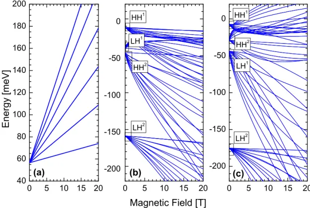
whereas at the valence band a strong hybridization takes place between holes as can be seen in Figure 2.2 (b) and (c). This coupling at the valence band depends not only on the spatial confinement or the magnetic field but also on the growth orientation, as expected [47].
0 5 10 15 20
40 60 80 100 120 140 160 180 200
0 5 10 15 20
-200 -150 -100 -50 0
0 5 10 15 20
-200 -150 -100 -50 0
E
n
e
r
g
y
[
m
e
V
]
(a) (b)
Magnetic Field [T] LH
2
HH
2
LH
1
HH
1
(c) LH
2
HH
2
LH
1
HH
1
Figure 2.2: Energy spectrum of the first six Landau levels in (a) conduction band, (b) valence band of a GaAs quantum well grown in (001) direction and (c) along the (113) direction. The superscript correspond to the subband m = 1,2. The predominant character of the carrier is indicated as HH or LH for heavy or light holes. It is noticeable the reorganization of hole subbands in (b) and (c) due to the different growth direction of GaAs quantum well.
2.3
Carrier-Phonon Interaction
these displacements, a polarized cloud surrounds the carrier during its displacement, and this carrier-phonon interaction is called polaron [48–50].
This quasi-particle can be described in terms of phonon absorption and phonon emis-sion. In polar crystals, the leading effects is triggered by the interaction with longitudinal-optical (LO) phonons 1 [51]. Under resonant conditions, when the energy difference
between two neighboring electronic states is about one LO-phonon energy, the polaron effects are enhanced and this can be tuned with magnetic fields.
The modifications expected in the Landau levels can be listed in the followings ways: the levels are shifted; the mass renormalization provokes changes in the levels form; anticrosings emerge between states |Ψi and |Ψi+~ω, where~ω is the phonon energy.
In order to know the effect of the electron-phonon and hole-phonon interaction on the energy levels, three different types of second-order perturbation methods were studied:
• the Rayleigh-Schr¨odinger perturbation theory [52],
• the Wigner-Brillouin perturbation method [52],
• and full diagonalization for degenerate states.
By including phonons in our electronic structure description, the wave function in-troduced before in (2.35) must include the number of phonons n, and takes the form
|Ψi=|ni|φxyzi|J, mJi. The annihilation and creation operations for phonons are ruled
by [16]
bq|ni=√n|ni, (2.42)
b†q|ni=√n+ 1|n+ 1i, (2.43) respectively, where q is the phonon wave vector.
To understand the hole-phonon interaction effects in 2D [53] we start by analyzing two contrasting contributions: the deformation potential theory and the Fr¨ohlich interac-tion. Let us first briefly discuss the contribution of the carrier-LO-phonons interaction
1There are two allowed frequencies of displacement know as the optical branch, and the acoustical
branch. Considering phonons belonging to the optical branch means considering the movement of
two atoms in the unit cell in opposite directions to each other, while in the acoustic mode they move
via deformation potentials [33], which is introduced by the Hamiltonian
HDP =
X
q
(MqU(q)bqeiq·r+h.c.), (2.44)
where Mq = (q·ǫq)
~
2ρωLOA
12
, ǫq is the polarization, ρ and A are the density and
area respectively, and U(q) is the deformation potential which is a model including scattering by transverse as well as longitudinal acoustic modes [54]. Still, one can prove that, up to second order, this interaction does not couple states in the conduction band, and the valence subbands in 2D can only be affected if the phonon is confined. Thus, this interaction will be dropped from our analysis.
In order to study the properties of charge carriers interacting with LO-phonons in systems with reduced dimensions, we used the Fr¨ohlich interaction that accounts for the carrier coupling with the polarization cloud in the lattice of polar crystals [55]. The effects can be described by treating the interaction as follows [16]
HI =
X
q
(Vqbqeiq·r+h.c.), (2.45)
where Vq is defined, in two dimension, as
Vq =−ı~ωLO
√
2πα Aq
!12
~
m∗ωLO
!14
, (2.46)
α= e
2
~
s
m∗
2~ωLO
1
ε∞ −
1
ε0
, (2.47)
α is called the Fr¨ohlich coupling constant, ε∞ and ε0 are the electronic and the static
dielectric constants, respectively. The second order correction can be obtained by [56]
Table 2.2: Phonon interaction parameters taken from ref [25]. Parameter Value
~ωLO 36.1eV
α 0.068
∆Eα =−
X
β
X
q
|hψβ|HI(q)|ψαi|2
Dβα
that can be interpreted as the polaron self-energy correction, where Dαβ is defined as
Dαβ =Eβ −Eα−~ωLO + ∆α. (2.49)
The common Rayleigh - Schr¨odinger (RS) model fixes ∆α = 0 and describes well the
ground state out of resonance when either|Eβ−Eα|<<~ωLOor|Eβ−Eα|>>~ωLO. In
turn, in the Wigner - Brillouin (WB) perturbation theory approaches ∆α= ∆Eα+iδ,
where the inter-dependence of the variables clearly requires a self-consistent solution, and δ is a vanishing imaginary part.
To evaluate the matrix element hψβ|HI(q)|ψαi, one can separate (2.45) into phonon
absorption Habs
I and emissionHIemi terms,
HI =HIabs+HIemi (2.50)
=X
q
Vqbqeiq·r+
X
q
Vq∗b†qe−iq·r. (2.51)
For absorption processes we have
hψβ|HIabs|ψαi=Vq
1
q1/2 hn
′|b
q|ni hJ′, m′J|J, mJihφ′xyz|eıq·r|φxyzi, (2.52)
where φxyz is the envelope function and has the following form
hφ′xyz|eıq·r|φxyzi=
Z ∞
−∞dx
e−12( x−x0
λc ) 2
e−
1 2
x−x′
0 λc
2
λc
√
2N−N′
N!N′!π e
ixqxH
N
x−x 0
λc
HN′
x−x′
0 λc ! ∗ ∗ Z ∞
−∞dy e
iykyeiyqye−iyk′y∗
∗ Z L
0 dzsin
mπ
L z
sin m′π
L z
!
eizqz. (2.53)
The analytical solution for all the integrals in hφ′
xyz|eıq·r|φxyzi is given by [57]
hφ′xyz|eıq·r
|φxyzi= 2
|N−N′|
2 min
s
N!
N′!,
s
N′!
N!
e
−λ2c 4
h
(ky−k′y) 2
+2(ky−k′y)iqx+q2x
i ∗
∗ L|min(N−NN,N′| ′) λ2
c
2
ky−ky′
2
+qx2
∗ " λ2 c 2
sgn (N −N′)
ky−ky′
+iqx
#|N−N′|
δm,m′δky−k′
y,qy, (2.54)
where Lα
n are the associated Laguerre polynomials, λc the magnetic length, and sgn
the signal function.
The probability amplitude for the absorption processes is given by
hψβ|H
abs I |ψαi
2
=δn′,n−1|hJ, m′J|J, mJi|2
X
q
Vq2q 1
q2 x+q2y
2|N−N′|min N!
N′!,
N′!
N!
!
δm,m′
e−λ
2 c
2 (q2x+qy2)
"
L|min(N−NN,N′| ′) λ2
c
2
qx2+q2y
#2"
λ2 c
4
qx2+iq2y
#|N−N′|
. (2.55) The sum over the phonon wave vector can be converted into integrals as P
q →
A (2π)2
R
dqxdqy,. In the case of 2D Landau levels, we were able to obtain analytic
solu-tions for these integrals [57]
A
(2π)2 Z
dqxdqy
hψβ|HIabs|ψαi
2
= min N!
N′!,
N′!
N!
!
δn′,n−1|hJ, m′J|J, mJi|2∗ A
(2π)2 V 2 q
Z ∞ 0
Z 2π
0 q⊥dq⊥dθ
1
q⊥ e
−λ2c 2 q2⊥
"
L|min(N−NN,N′| ′) λ2
c
2 q
2
⊥
#2"
λ2 c
2 q
2
⊥
#|N−N′|
δm,m′.
(2.56) The right side of equation (2.56) has an analytical solution, which leads to
X
q
hψβ|HIabs|ψαi
2
=δn′,n−1|hJ, m′J|J, mJi|2(~ωLO)2α
1
λc
s
~
4m∗ωLO
Γ1
2 +|N −N′|
Γ (1 +|N −N′|+ min (N, N′))
min (N, N′)! min (N, N′)!Γ (1 +|N −N′|)
dmin(N,N′) dhmin(N,N′)
F 1
2+|N−N′|
2 ,
3 4 +
|N−N′|
2 ; 1 +|N −N′|; 4h (1+h)2
(1 +h)1+|N−N′|1+h 1−h
12+|N−N′|
h=0 , (2.57)
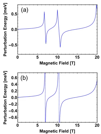
In Figure 2.3, we show the polaron self-energy correction ∆Eα calculated using (2.48),
for the fourth electronic state as a function of the magnetic field. The Figure 2.3(a) illus-trates the results obtained with the Wigner-Brillouin approximation and Figure 2.3(b) shows the Rayleigh-Schr¨odinger correction. Note that both WB and RS methods match far from resonance (at ∼ 7T and ∼10T). Naturally, in the RS approximation, Figure 2.3(b), divergences appear close to the resonant conditions Dα,β = 0 (when
Eβ −Eα−~ωLO = 0).
Figure 2.3: Energy correction calculated using (2.48) for the third conduction band state using (a) Wigner-Brillouin and (b) Rayleigh-Schr¨odinger method.
In the WB method ∆α = ∆Eα +iδ, this allows us to extract additional information
Figure 2.4: The imaginary part of the self-energy perturbed arise from the imaginary part of WB. δ= 0.001 meV.
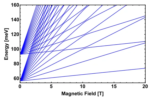
In resonant conditions, the electronic states capable to absorb one phonon become hybrid, and their lifetimes determine the total energy loss rate of carriers [32]. This has real implications in the carrier dynamics that will be explored in the next chapter. The RS and WB approximations do not give the actual pinning behavior of the electron energies out of resonance. For that reason we introduce the carrier-phonon interaction within thek·pmodel by using a full diagonalization. The fact that the energy states are fully quantized, supports this approach and we expand the Hamiltonian in (2.35) in the basis of|ψi=|0i|φxyzi|J, mJiand|ψi=|1i|φxyzi|J, mJifunctions. The corresponding
energy spectrum is obtained by diagonalizing the Hamiltonian including the electron-phonon interaction terms (2.52). As shown in Figure 2.5 for the conduction band, the anticrossings are produced at critical magnetic fields. These anticrossings correspond to the perfect hybridization of |ψi=|0i|φxyzi|J, mJi and |ψi =|1i|φxyzi|J, mJi states
which becomes a complementary interpretation of the increased life-time broadening of Landau levels discussed before.
We can see that the interaction with phonons modifies the system configuration but preserves the asymptotic behavior. The advantage of this approach is the perfect blending to the matrix format of the k·p and allows direct application to the study of these effects also in the valence subbands.
Figure 2.5: Conduction band levels corrected by full diagonalization. The upper branch corresponds to states with one phonon energy above E =Estates+~ωLO. The
zero energy is at the top of the valence band.
induced by polaron renormalization as seen from Figure 2.6.
Note that, according to equation (2.52), the Fr¨ohlich interaction allows the direct coupling only between states of the same character. However, because of the strong intraband mixing, the phonon interaction can couple the heavy and light hole levels. Other remarkable fact is the difference in the effective masses for the two growth direc-tions selected in the model, affecting the subbands relative position and subsequently the position of the hole-phonon resonances.
The effect is more vivid by increasing the quantum well width, as displayed in Figs. 2.7 and 2.8, calculated for twice large well (L = 100˚A). We understand that it can be difficult to elucidate details of the electronic structure within the mesh of valence band Landau levels. For that reason the energy spectrum is complemented with the information contained in the expansion coefficientsCN mof the respective hole states as
-200 -150 -100 -50
0 5 10 15 20 25 30 0 5 10 15 20 25 30
-200 -150 -100 -50 0
E
n
e
r
g
y
[
m
e
V
]
LH
1
-
LO
HH
1
-
LO
HH
1
LH
1
HH
2
Magnetic Field [T]
HH
2
-LO
LH
1
HH
1
-
LO
HH
2
HH
1
Figure 2.6: In red, the valence band energy levels for the [001] (left) and [113] (right) quantum well. The gray dot lines correspond to non phonon interaction case. At very low magnetic fields, the hole states are almost pure, but become hybrid as the external magnetic field, B, increases. The lowest energy levels with heavy and light hole characters are indicated in green (for spin up) and blue ( down spin). The width used is L = 50˚A and the super-index denotes the mth state due to the quantum well confinement.
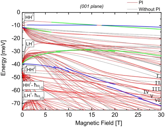
chosen to prove the main hypothesis that was risen in this part of the Thesis: the contributions of phonons to extra heavy and light-hole mixing. In Figs. 2.9 and 2.10, the weight coefficients of the wave functions are plotted as function of the magnetic field strength for the states highlighted in Figures 2.7 and 2.8, respectively. Solid curves represent the components with no phonon contribution while the dashed ones correspond to those involving one phonon. Note that at the regions of clear energy anticrossings, the phonon components assume a dominant role indicating that resonant hole-phonon coupling can take place between states with predominant heavy and light hole character. These features are also clearly spin-dependent.
sub-0 5 10 15 20 25 30 -70
-60 -50 -40 -30 -20 -10 0
III II
LH
1
-
LO
HH
1
-
LO
Without PI
HH
1
LH
1
HH
2
I
VI V
Magnetic Field [T]
PI (001 plane)
IV
E
n
e
r
g
y
[m
e
V
]
Figure 2.7: Energy spectrum obtained by an exact diagonalization of the HL+HI
(given by equations (2.35) and (2.45) respectivelly). The holes are confined in a GaAs quantum well grown on a (001) plane with L = 100˚A. The gray dot lines correspond to non phonon interaction case. Green lines (blue lines) correspond to states with a predominant contribution of the ground state of heavy or light holes with spin up (spin down). Highlighted lines are used to visualize phonons effects.
0 5 10 15 20 25 30 -70
-60 -50 -40 -30 -20 -10 0
PI
VI V
IV
III II
I
(113 plane)
HH
2
-
LO
LH
1
HH
1
-
LO
HH
2
E
n
e
r
g
y
[m
e
V
]
Magnetic Field [T]
Without PI
HH
1
Figure 2.9: Contribution of the main basis componentsCN mto the highlighted states
Figure 2.10: Contribution of the main basis components CN m to the highlighted
Spin-Resolved Photo-Generation
Filtering Induced by Phonon
Emission
The Stranski-Krastanov growth technique appears as a widespread method used to synthesize self-assembled quantum dots [58]. This growth mode, takes advantage of the lattice mismatch between different semiconductor compounds and takes place, in general, after the epitaxial deposition of a thin film referred as the wetting layer. The self-assembled quantum dots will subsequently grow on this surface.
The wetting layers allow controlling the strain fields that lead to the quantum dot formation and have unavoidable effects in their electronic structure and, in turn, affect the optical properties. One of the most intensely investigated quantum dot systems are those built on the basis of InGaAs alloys that have gained increasing importance in recent years due to their application in long-wavelength optoelectronic devices [43, 59]. In such systems, the spontaneous formation of InAs dots takes place after the deposition of a thin InGaAs wetting layer (that can be assumed as a two dimensional confinement layer) [60].
Considerable attention has been paid to the charge (and spin) dynamics that lead to the carrier capture in quantum dots and the role played by the wetting layers [61–66]. It is assumed, for instance, that in InGaAs quantum dots in a GaAs matrix, the carriers can be efficiently trapped in the quantum dots in both ways: (i) directly from
the matrix and (ii) via the wetting layer [67]. In particular, the optical injection of electron and hole spins into a quantum dot system is a fundamental tool for solid state quantum information processing. Like in single atoms, in quantum dots, spin polarization can be created by means of optical pumping with polarized light thanks to well defined optical selection rules. The selection rules determine the exchange of angular momentum between incoming photons and a quantum state comprising one or several electrons and holes. In the most general case, light absorbed by a quantum dot creates a superposition of spin up and spin down states, thus reducing the maximum attainable spin polarization. Yet, there are special situations where the selection rules allow a 100 percent spin polarization using circularly polarized light.
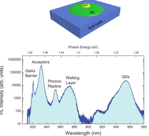
In general, to attain high degree of spin polarization and long term spin coherence, re-sonant excitation conditions are chosen. Near rere-sonant excitation energy of the relevant spin states, the angular momentum transfer is maximized as well as the coherence be-tween photons and spins. The dynamics of the just created spin is governed in this case by pure spin dephasing mechanisms like anisotropic exchange interaction and hyper-fine coupling [68]. Non resonant spin injection mechanisms, on the other hand, involve optical selection rules for the excited states and additional spin relaxation processes. Thus, the non-resonant pathways for optical spin injection have been traditionally dis-regarded in favor of the resonant ones, however these avoid intermediary mechanisms or states that could be exploited for filtering phenomena such as spin-bottleneck [69, 70]. In this chapter, we investigate an unexplored nonresonant pathway to inject oriented spins from high energy extended bulk states into localized InGaAs/GaAs quantum dot states. The sample studied is represented in the upper diagram of Figure 3.1. The carrier relaxation path was assessed through the sample photoluminescence that allows observing the emission lines from practically all the intermediary steps from the bulk states towards those confined in the quantum dots as shown in the lower panel of Figure 3.1.
sam-Figure 3.1: Upper panel: sketch of the various layers of the structure under study. Lower panel: photo-luminescence spectrum of the sample labeling the various contri-butions provided by the collaborators at the Micro-electronics Institute of Madrid.
ples used in this study were grown and characterized by our colleagues at the Micro-electronics Institute of Madrid, Spain. Undoped substrates were used and the growth conditions were optimized for low quantum dot density and emission wavelength around 980 nm.
To investigate the spin dynamics the samples were embedded in a cryogen-free cryostat and investigated by magneto-photoluminescence (PL) in back-scattering Faraday con-figuration at low temperature (4-77 K). For single quantum dot investigation a confocal micro-PL setup was used.
Figure 3.2: (a-c) Photoluminescence spectra obtained with no magnetic field applied at T=4.2K for the GaAs band edge, ensemble quantum dot ground state and single quantum dot neutral exciton. Contour plots of the emission as function of the magnetic field in each spectral region is showed in the lower panels. Panels (d)(f) stand for experiments done with continuous wave laser excitation of energy EL= 1.797eV, coming
from a temperature stabilized laser diode emitting at 690.0nm with power stability better than 2 %. Correspondingly, panels (e)(g)(h) stand for experiments done with EL
= 1.579eV. Courtesy of our collaborators at the Micro-electronics Institute of Madrid.
experiments done with continuous wave laser excitation of energy EL = 1.797eV com-ing from a temperature stabilized laser diode emittcom-ing at 690.0nm with power stability better than 2%. Correspondingly, Figure. 3.2 (e)(g)(h) stand for experiments done with a CW laser diode stabilized at 785.0nm (EL = 1.579eV). Both lasers were linearly polarized and continuously monitored to normalize the emission intensity by the laser power. In both situations, well-known diamagnetic and zeeman (orbital and spin) en-ergy shifts can be identified for each transition which do not depend on the excitation energy. Yet, both excitation energies, being above the GaAs band edge, result in a very different evolution of the integrated PL intensity and degree of circular polarization. For the laser with energy EL = 1.579eV, theσ+andσ−components of the emitted light
show sharp resonances with1/Bperiodicity as shown in Fig. 3.2 (e)(g). The oscillations
can be mapped down to the single quantum dot level resulting in brighter spots in the parabolic dispersion of the neutral exciton shown in Figure 3.2 (h). Both the optical excitation and detection were performed by controlling the light polarization (either linear or circular), thus spin contributions were optically resolved as a function of B. The period and amplitude of these oscillations can be better analyzed integrating the
σ+ and σ− intensities as a function of B and normalizing to their values at 0T. The
panels in Figure 3.3 show the results obtained for the ensemble quantum dot and GaAs band edge. Given the selection rules at play in III-V semiconductors, an imbalance of the σ+ and σ− emission intensity reflects an unequal population of spin-up and
spin-down electrons.
In panels (a) and (b) of Figure 3.3 one may note that the magnetic field resonances disappear (dashed lines) once the incident laser energy is shifted beyond certain reso-nance threshold. Another interesting feature that can be noticed is the fact that, for the GaAs band edge, all the resonances appear regardless the polarization configura-tion for excitaconfigura-tion and collecconfigura-tion. However, for the quantum dots this is no longer the case when a linearly polarized light is used and a clear spin filtering takes place, Figure 3.3(a).
For excitation with circularly polarized light, it is possible to map the transitions emis-sion for both σ+ and σ− independently of the collection as showed in Figure 3.3(c-f).
condi-50 75 100
75 100 125 150
50 75 100 125
50 100 150 200
75 100 125
0 2 4 6 8
50 100 150 200
b) a)
L
s
-QD
GaAs
E
L
=1.579eV
E
L
=1.797eV
L
-L +
QD
GaAs
+
-+ +
QD
GaAs
-
-- +
I
P
L
n
o
r
m
(
%
)
c)
d)
e)
e)
Magnetic Field (T)
Figure 3.3: Integrated bulk and quantum dot photoluminescence intensities as a function of B. The polarization configuration for excitation and collection is denoted by σα and Lσα where L stands for linearly polarized excitation. The spectra are
normalized to the values at 0T.
tions are satisfied. Besides, one should note that the maxima in Figure 3.3 (c-d) are shifted with respect to those in Figure 3.3 (e-f).
3.1
Theoretical Simulation
By analyzing the optical response in this kind of connected systems (due to the growth conditions bulk/wetting layer/quantum dot appear in sequence) when a magnetic field is applied, two challenging questions arise: what is the potential interference of 2D Landau levels in the wetting layer for the relaxation from bulk 3D states towards fully
confined states in quantum dots and is there a potential phonon assistance?
Thus, we build the Figure 3.4 to illustrate the carrier dynamics in the structure, where the dashed arrows correspond to the optical excitation and emission, whereas the con-tinuous arrows represent the relaxation processes that ultimately result in the quantum dot emission. Both the optical excitation and detection were performed by controlling the light polarization (either linear or circular), thus spin contributions were optically resolved.
Figure 3.4: Upper panel: sketch of the potential profile of a system Bulk/wetting layer (WL)/quantum dot (QD). Lower panel: schematic representation of the spin-resolved dynamics.

![Figure 2.6: In red, the valence band energy levels for the [001] (left) and [113] (right) quantum well](https://thumb-eu.123doks.com/thumbv2/123dok_br/15914024.673971/41.892.158.802.116.562/figure-valence-band-energy-levels-left-right-quantum.webp)

![Figure 2.9: Contribution of the main basis components C N m to the highlighted states of Figure 2.7 for a quantum well grown along [001] direction](https://thumb-eu.123doks.com/thumbv2/123dok_br/15914024.673971/44.892.107.720.260.904/figure-contribution-components-highlighted-states-figure-quantum-direction.webp)
![Figure 2.10: Contribution of the main basis components C N m to the highlighted states of Figure 2.8 for a quantum well grown along [113] direction](https://thumb-eu.123doks.com/thumbv2/123dok_br/15914024.673971/45.892.172.786.273.894/figure-contribution-components-highlighted-states-figure-quantum-direction.webp)