Isabel Carina Simões da Silva
Biological characterization of coatings
based on titanium dioxide doped with
metallic elements for antimicrobial
applications
13
Isabel Carina Simões da Silva
Biological characterization of coatings based on tit
anium dio
xide doped wit
h me
Trabalho realizado sob a orientação do
Professor Doutor Joaquim Carneiro
Isabel Carina Simões da Silva
Dissertação de Mestrado
Mestrado em Biofísica e Bionanossistemas
Biological characterization of coatings
based on titanium dioxide doped with
metallic elements for antimicrobial
applications
AGRADECIMENTOS
Todo o meu trabalho de investigação não teria sido possível sem a presença de fantásticas pessoas que me acompanharam ao longo deste percurso. Um muito obrigado não chegará para agradecer todo o apoio, dedicação e respeito que sempre demonstraram por mim e pelo meu trabalho.
Em primeiro quero agradecer aos meus orientadores, Professor Doutor Joaquim Carneiro do Departamento de Física, e Professora Doutora Célia Pais do Departamento de Biologia, da Universidade do Minho, por toda a dedicação, disponibilidade e apoio incansável que sempre me demonstraram. Por toda a bondade e conhecimento que me conseguiram transmitir tão claramente. Aumentaram ainda mais o meu gosto pela investigação onde descobri uma área fascinante: a nanotecnologia.
Gostaria também de agradecer à Professora Doutora Paula Sampaio do Departamento de Biologia e ao Doutor Pedro Carvalho do Departamento de Física, da Universidade do Minho. Foram como meus segundos orientadores devido ao facto de estarem constantemente presentes em cada barreira e desafio, sempre prestáveis a me apoiar e ajudar.
Quero agradecer também à Universidade do Minho, ao Departamento de Física e ao Departamento de Biologia pela disponibilidade na realização deste meu trabalho.
É com enorme agrado que agradeço à Mestre Sofia Azevedo do Departamento de Física da Universidade do Minho, pelo trabalho incansável para comigo, pela força, determinação, empenho e conhecimento extraordinário que possui e demonstrou-‐ me a cada passinho. Pelos “sermões” que nunca me faltaram mas também pelas palavras de incentivo: Fizeram falta!
Aos meus colegas do Departamento de Biologia da Universidade do Minho, Catarina Carneiro, Catarina Vaz, Joana Pereira, Filipa Vale e Manoel Oliveira que me acolheram de braços abertos de forma tão sincera e calorosa no seu espacinho onde todos tínhamos a mesma paixão e gosto pela investigação. Por toda a amizade e cumplicidade que se formou ao longo deste percurso. “A “Micro II” é a nossa segunda casa”.
Quero agradecer também a todos os técnicos, tanto do Departamento de Física como do de Biologia, que sempre estiveram presentes para me ajudar no que necessitava. Agradeço principalmente à técnica Manuela Rodrigues, do Departamento de Biologia, pelo fornecimento dos microorganismos que utilizei neste trabalho e ao Engenheiro José Santos, do laboratório de filmes finos II do Departamento de Física, pelo apoio e presença constante no laboratório!
Como é óbvio quero agradecer aos meus colegas de mestrado, Rita Rodrigues, Henrique Cachetas, Ivo Lopes, José do Egipto, Jorge Rodrigues, João Martins e Pedro Mendes. Este obrigado é por estes dois anos onde nos aprofundamos em tantos conhecimentos, pelas tardes e noites de trabalhos intensos, pela força e determinação que cada um me demonstrou à sua maneira. Pelas gargalhadas e simpatia que nunca faltou neste grupo. Desde já desejo a maior sorte a todos vocês!
E por fim mas não menos importante, muito pelo contrário, quero agradecer à minha família, especialmente às três pessoas mais importantes da minha vida, à minha mãe Ana, ao meu pai Alberto e ao meu irmão Carlos, por nunca me desampararem em nenhum momento, por tanto esforço e coragem, por tanto amor e carinho e principalmente por sempre acreditarem em mim e naquilo que sonho. Um agradecimento especial ao Tiago por estar ao meu lado constantemente e por compreender e ouvir sempre os meus desvaneios e mau humor com palavras de incentivo e força. Vocês são o meu porto de abrigo.
A todos eles o meu sincero Obrigado!
ABSTRACT
The use of semiconductors for processes of self-‐cleaning, air and water depollution as well as surface disinfection has triggered a great interest in the scientific community. One of the most used semiconductor materials is titanium dioxide (TiO2) due to their large
photocatalytic effect, higher oxidation strength, chemical stability non-‐toxicity and availability, among others. This oxide has been highly researched and was found that it is capable of decomposing various organic and inorganic compounds.
Most of these studies were conducted under ultraviolet light (UV), since TiO2 has a
photocatalytic activity and a relatively high chemical stability under UV radiation. The process has several advantages and one of them is the ability to combine processes involving biological decontamination methods, which makes this semiconductor capable of removing a wide range of bacteria, viruses, fungi, algae, protozoa, etc. (antimicrobial effect).
Despite the advantages of this process we can notice two important limitations. Firstly, only 5% of the solar spectrum comprises ultraviolet radiation; secondly, the direct UV radiation is harmful to human’s health. Based on these limitations, the researchers have been studying methods that enable the use of TiO2 under the presence of visible light. This
effect can be achieved by doping TiO2 with some metallic elements. Having this in mind
some research groups have been focusing on the antimicrobial applications of this semiconductor material. Thus, the main goal of this work was the production of TiO2 thin
films and TiO2 thin films doped with two different metals (iron and silver) with
photocatalytic activity and, consequently, antimicrobial proprieties.
The thin films were deposited on glass and cotton substrates by DC magnetron sputtering method. The studies of morphological characterization of the surface were performed using SEM and AFM techniques. The thin films crystalline structure was evaluated by XRD technique. Through UV-‐Vis spectroscopy it was possible to study their optical proprieties
RESUMO
A utilização de semicondutores para processos de auto-‐limpeza, desinfecção de superfícies, do ar e da água, tem suscitado um grande interesse no mundo científico. Um dos semicondutores mais utilizado é o dióxido de titânio (TiO2) devido ao seu elevado
efeito fotocatalítico, elevada capacidade de oxidação, estabilidade química, disponibilidade e não-‐toxicidade, entre outros. Este material semicondutor tem sido extremamente investigado e verificou-‐se que é capaz de decompor vários tipos de compostos orgânicos e inorgânicos.
A maioria destes estudos foram realizados sob a ação de luz ultravioleta (UV), uma vez que o TiO2 apresenta uma actividade fotocatalítica e uma estabilidade química relativamente
elevada sob a radiação UV. O processo apresenta diversas vantagens sendo uma delas a possibilidade de combinar processos de descontaminação biológica, tornando este semicondutor capaz de eliminar uma vasta gama de bactérias, vírus, fungos, algas, protozoários, etc. (efeito antimicrobiano).
Embora o processo apresente diversas vantagens, observam-‐se duas importantes limitações. Em primeiro lugar, apenas 5% do espectro solar compreende a radiação ultra-‐ violeta, e em segundo lugar a radiação UV é prejudicial para a saúde do ser humano. Tendo em consideração estas limitações, vários grupos de investigação têm estudado métodos alternativos que possam ser capazes de permitir a utilização de TiO2 na presença da luz
visível. Um dos métodos utilizados consiste na dopagem do TiO2 com elementos metálicos.
Tendo em consideração o exposto, alguns grupos de investigação têm direcionado os seus trabalhos na utilização deste material semicondutor ao estudo de aplicações antimicrobianas. Neste sentido, o principal objetivo deste trabalho visou a produção de filmes finos de TiO2 e filmes finos de TiO2 dopados com dois metais diferentes (ferro e
prata) com atividade fotocatalítica e propriedades antimicrobianas.
Os filmes finos foram depositados em substratos de vidro e de algodão pelo método de pulverização catódica em magnetrão utilizando fonte DC. Os estudos de caracterização morfológica da superfície foram realizados pela utilização de microscopia electrónica de varrimento (do inglês Scanning Electron Microscopy, SEM) e microscopia de força atómica (do inglês Atomic Force Microscopy, AFM). A estrutura cristalina dos filmes finos foi avaliada pela técnica de Difração de Raios-‐X (do inglês X-‐ray difraction, XRD).
Através da utilização dr espectroscopia UV-‐Vis foi possível estudar as propriedades ópticas dos filmes finos produzidos (nomeadamente a transmitância). A atividade
TABLE OF CONTENTS
AGRADECIMENTOS ... vii
ABSTRACT ... ix
RESUMO ... xi
LIST OF ABBREVIATIONS AND SYMBOLS ... xv
LIST OF FIGURES ... xix
LIST OF TABLES ... xxiii
CHAPTER I – INTRODUCTION ... 3
1.1 – GENERAL ... 3
1.2 – MOTIVATION AND OBJECTIVES ... 9
1.3 – THESIS ORGANIZATION ... 9
CHAPTER II – BIBLIOGRAPHIC REVIEW ... 13
2.1 – INTRODUCTION ... 13
2.2 – SEMICONDUCTORS ... 13
2.3 – TITANIUM DIOXIDE ... 15
2.3.1 – GENERAL DESCRIPTION ... 15
2.3.2 – PHOTOCATALYTIC PROPERTIES ... 17
2.3.3 – APPLICATIONS OF TIO2 COATINGS ... 21
CHAPTER III – PRODUCTION TECHNIQUES ... 27
3.1 – INTRODUCTION ... 27
3.2 – PHYSICAL VAPOR DEPOSITION (PVD) ... 27
3.2.1 – SPUTTERING TECHNIQUE ... 28
3. 3 – FILM GROWTH ... 33
CHAPTER IV – CHARACTERIZATION TECHNIQUES ... 41
4.1 – INTRODUCTION ... 41
4.2 – STRUCTURAL PROPERTIES ... 41
4.2.1 – X-‐RAY DIFFRACTION (XRD) ... 41
4. 3 – SURFACE PROPERTIES ... 43
4.3.1 – SCANNING ELECTRON MICROSCOPY (SEM) ... 43
4.3.2 – ATOMIC FORCE MICROSCOPY (AFM) ... 46
CHAPTER VI – RESULTS AND DISCUSSION ... 65
6. 1 – X-‐RAY DIFFRACTION (XRD) ... 65
6. 2 – MORPHOLOGICAL CHARACTERIZATION OF THE THIN FILMS ... 66
6. 3 – OPTICAL SPECTROPHOTOMETRY ... 74
6. 4 – PHOTOCATALYTIC ACTIVITY ... 77
6. 5 – ANTIMICROBIAL ACTIVITY ... 80
6. 6 – METALIC TO OXIDE MODE ... 84
6. 7 – XRD – X-‐Ray Diffraction ... 85 6. 8 – MORPHOLOGICAL CHARACTERIZATION ... 86 6. 9 – OPTICAL SPECTROPHOTOMETRY ... 90 6. 10 – CONTACT ANGLE ... 92 6.11 – PHOTOCATALYTIC ACTIVITY ... 94 6. 12 – ANTIMICROBIAL ACTIVITY ... 96
CHAPTER VII – CONCLUSIONS ... 101
CHAPTER VIII – FUTURE PERSPECTIVES ... 105
REFERENCES ... 107
LIST OF ABBREVIATIONS AND SYMBOLS
μm Micrometer
AFM Atomic Force Microscopy Ag Silver
Al203 Aluminum Oxide or Alumina
Ar Argon Au Gold
BSE Backscattered electrons C Carbon
CB Conduction Band
CBM Conventional balanced magnetrons CO2 Carbon Dioxide
Cu Copper
CVD Chemical Vapor Deposition DC Direct Current
DNA Deoxyribonucleic Acid DRIs Device-‐Related Infections
E. Coli Escherichia coli
EDX Energy Dispersive X-‐ray Eg Band Gap Energy
H2O2 Hydrogen Peroxide
IM Inner Membrane LB Luria-‐Bertani medium M Metal
MB Methylene blue N Outer magnet NaCl Sodium Chloride Nd Neodymium Ni Nickel NiO Nickel Oxide nm Nanometer NPs Nanoparticles O2-‐ Superoxide Radical
OH Hydroxyl Radical OOH Hydroperoxyl OM Outer Membrane Pd Palladium
PG Peptidoglycan PM Planar magnetron
PVD Physical Vapor Deposition PZC Point of zero charge RF Radio frequency
ROS Reactive Oxygen Species S Inner magnet
SC Semiconductor SE Secondary electrons
SEM Scanning Electron Microscopy Si3N4 Silicon nitride
SiO2 Silicon Dioxide or Silica
Sn Tin
SPM Scanning probe microscopes STM Scanning tunneling microscopy SZM Structure zones models
Th Homologous temperature
Tm Melting temperature
Ts Temperature normalized
TiO2 Titanium Dioxide or Titania
UBM Unbalanced magnetrons UV Ultraviolet
UVA Ultraviolet Type A
UV-‐Vis-‐Nir Ultraviolet-‐Visible-‐Near Infra-‐Red zone VB Valence Band
XRD X-‐Ray Diffraction ZnO Zinc Oxide
ZrO2 Zirconium Dioxide or Zirconia
hυ Photon energy e-‐ Electron
γSV Tensions between solid and vapor
γLV Tensions between liquid and vapor
λ Wavelength F Force
K Spring Constant T Transmittance A Absorbance TA Total surface area cm Centimeters W Walt V Volt η Yield k Photodegradation rate
LIST OF FIGURES
Figure 1: Representation of the dimensions of some typical species, in its various
scales (adapted from [2]). ... 3
Figure 2: Thin films in glass and sunglasses [4, 5]. ... 4
Figure 3: TiO2 thin film in glass substrate. ... 5
Figure 4: Illustration of the formation of a biofilm. ... 7
Figure 5: Schematic view of various methods for surface modification of medical devices with antibacterial properties [21]. ... 8
Figure 6: Schematic representation of a semiconductor [25]. ... 14
Figure 7: Schematic representation of a semiconductor after photon-‐irradiation [25]. ... 14
Figure 8: TiO2 phases rutile (a), anatase (b) and brookite (c) (Ti (white); O (red)) [30]. ... 16
Figure 9: Image illustrating the photocatalytic mechanism of TiO2 after UV light absorption ... 18
Figure 10: The graph shows increasing number of publications on photocatalytic disinfection over the years [46]. ... 21
Figure 11: Electron microscopy of E. coli bacteria [71]. ... 22
Figure 12: Cell walls of gram-‐negative (A) and gram-‐positive (B) bacteria [72]. ... 22
Figure 13: Role of ROS in photocatalytic killing of bacteria [46]. ... 23
Figure 14: Scheme of the photocatalytic degradation process of E. coli representing the different steps in contact with TiO2 thin films [85]. ... 24
Figure 15: Schematic representation of a sputtering process [96]. ... 29
Figure 16: Bombarding of the argon atoms on the target surface and therefore electron emission [97]. ... 30
Figure 22: Illustrations of the three types of thin film growth including (a) Volmer-‐ Weber (island growth), (b) Frank-‐van der Merwe (layer-‐by-‐layer growth), and
(c) Stranski-‐Krastanov (mixed island-‐layer growth) growth [108]. ... 35
Figure 23: Schematic representation for the structure zone model proposed by Movchan and Demchishin. The micro-‐structure of the metal film is divided into three structure zones by the melting temperatures T1 = 0.3 and T2 = 0.5 [109].36 Figure 24: Schematic representation of Thornton's Model (left) and its modification by Messier (right). ... 36
Figure 25: Diffractograms of a XRD result of a TiO2 sample [45]. ... 42
Figure 26: Schematic of diffraction according to Bragg’s law. ... 43
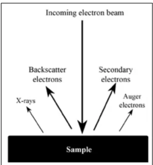
Figure 27: Image showing the Scanning Electron Microscopy equipment. ... 44
Figure 28: Signals generated by the incidence of the electron beam on the sample surface. ... 45
Figure 29: Typical EDX spectrum of a sample of TiO2. When are present the respective peaks of Titanium (Ti) and oxygen (O). The Carbon (C), Gold (Au) and palladium (Pd) peaks may also be observed [113]. ... 46
Figure 30: Different types of tips of the AFM technique. ... 47
Figure 31: Principle of operation of an AFM ... 48
Figure 32: Example of a result obtained after analysis by AFM technique [45]. ... 48
Figure 33: The angle between the tangent line at the contact point and the horizontal line of the solid surface. ... 49
Figure 34: Formation of the angle through the contact between the sample surface and a liquid at the three phase boundary: (a) high values of the 90º (θ>90º), (b) low values of the 90º (θ<90º) and (c) when the angle θ=90º. ... 50
Figure 35: Electromagnetic spectrum. [130]. ... 51
Figure 36: Transmittance spectrum of TiO2 and Fe-‐TiO2 samples [55]. ... 52
Figure 37: Schematic representation showing the incidence of light on a sample. When light meets an interface, a portion of it will be reflected, and the rest will pass into the incident medium and get refracted. ... 52
Figure 38: Representative scheme of the reactive magnetron sputtering system used to produce TiO2 based thin films (left) [45]. Photographic image of the system (right). ... 55
Figure 39: (a) Image of the inside of the deposition chamber; (b) Electrical system and a control unit; (c) Deposition gases. ... 56
Figure 40: Diffraction system used to determine the structural properties of the produced TiO2 thin films. ... 59 Figure 41: Scanning Electron Microscopy used to study surface properties of thin
films. ... 59 Figure 42: Atomic Force Microscopy used to study roughness of thin films. ... 59 Figure 43: X-‐Ray Diffraction Spectra of TiO2 thin films and Fe – and Ag – doped TiO2
thin films by the Bragg Brentano method. ... 65 Figure 44: Surface SEM micrographs of TiO2 thin films deposited with different
deposition times: 1 hour (a) magnification of 50 000x, (b) magnification of 200 000x and (c) EDX spectrum; 3 hour (d) magnification of 50 000x, (e)
magnification of 200 000x and (f) EDX spectrum. ... 66 Figure 45: AFM images of the TiO2 thin films produced by using different deposition
times: 1hour (a) 2D; (b) 3D and 3hours (c) 2D; (d) 3D. ... 67 Figure 46: SEM micrograph and EDX spectrum of Fe-‐ doped TiO2 thin films produced
with different deposition times: 1 hour (a) magnification of 50 000x, (b)
magnification of 200 000x and (c) EDX spectrum; 3 hour (d) magnification of 50 000x, (e) magnification of 200 000x and (f) EDX spectrum. ... 68 Figure 47: AFM images of the Fe-‐doped TiO2 thin films produced by using different
deposition times: 1hour (a) 2D; (b) 3D and 3hours (c) 2D; (d) 3D. ... 69 Figure 48: SEM micrograph and EDX spectrum of Ag-‐ doped TiO2 thin films produced
with different deposition times: 1 hour (a) magnification of 50 000x, (b)
magnification of 200 000x and (c) EDX spectrum; 3 hour (d) magnification of 50 000x, (e) magnification of 200 000x and (f) EDX spectrum. ... 70 Figure 49: AFM images for samples Ag-‐ doped TiO2 thin films produced by using
different deposition times: 1hour (a) 2D; (b) 3D and 3hours (c) 2D; (d) 3D. ... 72 Figure 50: Cross-‐section SEM micrograph of TiO2 thin films produced during 1h. .... 73 Figure 51: Cross-‐section SEM micrographs of Fe-‐ doped TiO2 thin films deposited
during (a) 1 hour and (b) 3 hours. ... 73 Figure 52: Cross-‐section SEM micrographs of Ag-‐ doped TiO2 thin films deposited
Figure 55: Absorption spectra of the MB aqueous solution over time under UV irradiation the photocatalytic action of Ag-‐ doped TiO2 thin films deposited during 1 hour. ... 77 Figure 56: MB photodegradation yield and k values under UV irradiation and the
action of (a) TiO2, (b) Fe-‐ doped TiO2 and (c) Ag-‐doped thin films. ... 79 Figure 57: E. coli HB 101 growth curves obtained in the presence of (a) TiO2 thin
films and (b) in the presence of Fe-‐doped thin films. ... 81 Figure 58: E. coli HB 101 growth curves obtained in the presence and in the absence
of Ag-‐doped thin films. ... 82 Figure 59: Discharge voltage at different oxygen flow for three different argon flow
rates (5sccm, 15sccm and 30sccm) during DC reactive magnetron sputtering (discharge current was 0,45 A, reverse time was 2µs and frequency was
100kHz). ... 84 Figure 60: XRD Diffraction of TiO2 thin films by the Bragg Brentano method. ... 85 Figure 61: SEM micrograph for TiO2 samples with 30minutes of the deposition time
in different argon flow: A11 – 5sccm (a) magnification of 50 000x, (b) magnification of 200 000x and (c) cross section; A14 – 30 sccm (d)
magnification of 50 000x, (e) magnification of 200 000x, (f) cross section and (g) detail of the thin film morphology – A14. Red numbers indicate the
thickness of the film. ... 86 Figure 62: AFM images for samples TiO2 thin films produced by using 30min of the
deposition time and different argon flows: A11 – 5sccm (a) 2D; (b) 3D and A14 – 30sccm (c) 2D; (d) 3D. ... 87 Figure 63: SEM micrograph for TiO2 samples with 120minutes of the deposition time
in different argon flow: A15 – 5sccm (a) magnification of 50 000x, (b) magnification of 200 000x and (c) cross section; A17 – 30 sccm (d)
magnification of 50 000x, (e) magnification of 200 000x, (f) cross section ... 88 Figure 64: EDX spectrum for TiO2 samples in the different argon flows (a) 5 sccm
(A15) and (b) 30 sccm (A17). ... 89 Figure 65: AFM images for TiO2 thin films produced by using a deposition time of
120min at different argon flow rates: A15 – 5sccm (a) 2D; (b) 3D and A17 – 30sccm (c) 2D; (d) 3D. ... 90 Figure 66: UV-‐Vis-‐NIR transmittance spectra of samples with argon flow 5sccm and
30sccm for 30min (a) and 120min (b). ... 91 Figure 67: Images of the water droplet form deposited on the sample surface after
90s. ... 93 Figure 68: Contact angle variation over time. ... 94
Figure 69: Photocatalytic degradation of methylene blue aqueous solution on A11, A14, A15 and A17 samples under UV light source (C0 is the initial aqueous RhB concentration, 0,5 mg/l and C is the aqueous RhB concentration after 15, 30, 60, 90, 120, 150, 180, 210 and 240 min irradiation time). ... 95 Figure 70: Photographs of the petri dishes showing E. coli growth under different
conditions: in the control, in contact with the glass and A15, after 2hours and 4 hours of UV irradiation. ... 97 Figure 71: Photographs of the petri dishes showing E. coli growth under different
conditions: in the control, in contact with the glass and A17, after 2hours and 4 hours of the UV irradiation. ... 97
LIST OF TABLES
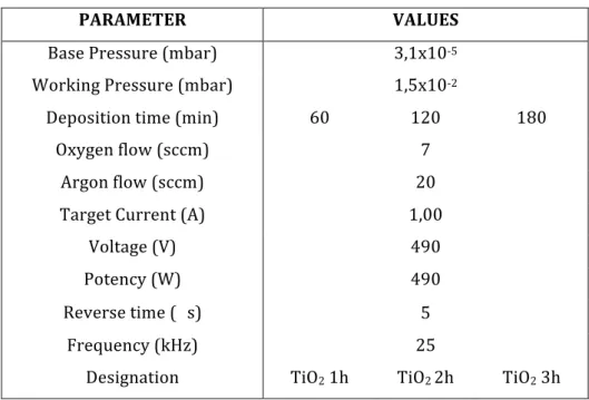
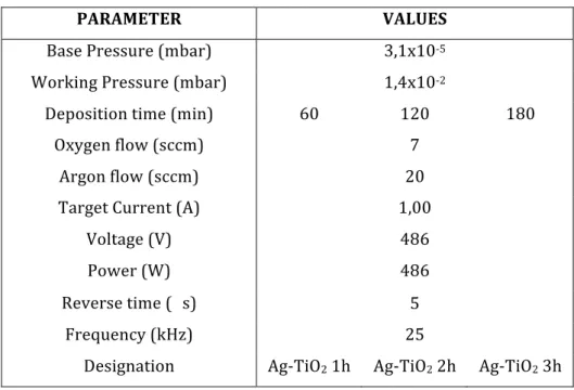
Table 1: Sputtering deposition parameters for the TiO2 thin films samples. ... 57 Table 2: Sputtering deposition parameters for the Fe-‐TiO2 thin films samples. ... 57 Table 3: Sputtering deposition parameters for the Ag-‐TiO2 thin films samples. ... 58 Table 4: Sputtering deposition parameters for the TiO2 thin films samples. ... 58 Table 5: Roughness values for all the produced samples. ... 72 Table 6 – Summary of the calculated thicknesses for all the produced samples. ... 75 Table 7: Sputtering deposition parameters for the TiO2 thin films samples. ... 83 Table 8: Thicknesses of the samples A11, A14, A15 and A17. ... 92 Table 9: Values obtained of the yield (%) and the rate constant of photodegradation
in different coatings. ... 95
CHAPTER I
INTRODUCTION AND OBJECTIVES
CHAPTER I – INTRODUCTION
1.1 – GENERAL
The origin of Nanotechnology dates back to 1959, where Richard Freynman proposed the direct manipulation of individual atoms as a very powerful physico-‐ chemical tool very powerful. However, the term nanotechnology was created by Norio Taniguchi of Tokyo University, in 1974. This term was defined as the precision production of materials with nanometer scale. Furthermore, Eric Drexler in 1986, mentioned the term "nanotechnology" in his book "Engines of Creation: The Coming Era of Nanotechnology" [1].
Nanotechnology studies the characterization, production and application of structures, equipment, devices and systems in scale ranging from individual molecules or molecules of approximately 100 nanometers, as well as the junction of the nanostructures for systems with larger dimensions [1].
A nanometer (nm) is one thousand millionth of a meter. The size of a DNA molecule is in the range of 100 nm and is slightly lower than that of a virus. A single human hair is about 80,000nm diameter. A red blood cell is approximately 7,000 nm wide diameter and water molecule almost 0.3nm [2]. See the comparison of scale in Figure 1.
Nanomaterials have been used over time in various applications ranging from window glass and sunglasses lens (see Figure 2) to car bumpers and paints. Nowadays, applications have increased in several areas, such as the manufacture of other materials, computers chips, in medical diagnosis and health care, biotechnology, exploration, security, energy, among others [3].
In the next 10 to 15 years, nanotechnology will have a significant impact on the economy and society, and ever more with utmost importance so that new scientific and technological advances are achieved.
Figure 2: Thin films in glass and sunglasses [4, 5].
Currently, scientific research in the field of nanotechnology has attracted growing interest because of its several applications, either through design of new products, materials characterization, production and application of structures, devices and systems in nanometer scale [6, 7].
In fact, applications of nanomaterials, especially of nanoparticles (NPs), in areas related to therapeutics and diagnosis, such as pathogen detection, drug delivery, disease diagnosis and imaging, among others, are in continuous progress. Alongside with the nanoparticles, thin films coatings have been used to design and create advanced nanocoating systems with significantly optimized or enhanced properties of great interest to health, food and biomedical industry [8].
Thin films are use for more than half a century. Their applications are found in the making of electronic devices, instrument coating, optical coatings and decorative parts.
Initially the thin films were used for decorative effects but currently these coatings are used for materials protection and manufacture of sensors, conductors, resistors of microelectronic circuits [9]; protection of metals against corrosion [10]; solid lubricants [11]; are also used to the protection of plastic packaging for food and optical coatings [12]; tool coatings to enhance their hardness [13]; photovoltaic devices for solar energy conversion [14], among many other applications.
The name "thin film" is given to a coating with thickness of up to 300 µm, but this doesn’t include coatings of paints and varnishes that, in general, are ticker. These coatings can be made from various types of materials, including metals, metal oxides or organic substances [15]. In Figure 3 is shown a thin film of a metal oxide -‐ TiO2, in glass substrate.
Ø Should be strongly adherent to the surface (substrate), since they are extremely fragile;
Ø Should have a uniform thickness;
Ø Must be pure or have controllable composition; Ø Should have low defect density [16].
Normally the properties of a material in the form of a thin film differ substantially from the properties of the same material in its solid state due to the influence of the surface, the relation between surface and volume is much greater in the case of the film. On the other hand thin films properties depends on the deposition processes that are used [15]. Thin films can be obtained by a variety of techniques, such as: deposition from liquids; chemical deposition from the vapor phase, a process called CVD (Chemical Vapor Deposition); and by physical deposition from the vapor phase, a process denominated PVD (Physical Vapor Deposition). In this last case species are physically torn apart from a target by temperature (evaporation) or by impact of ions (Sputtering) and are transported to the substrate where they condense into a thin film [15].
In Chapter III Sputtering process will be explained in detail, since the process was used in this laboratory work for the production of thin films.
Since 2010, nanotechnology use became common in many manufactured goods, for example, in electronics and informatics applications, as the production of microprocessors and memory chips, which became available in the market in 2009. Finally, the applications in health-‐care became more significant with the application of the nano-‐enabled pharmaceuticals and medical devices [17]. These devices have become of greater importance for human health care and, because of that, its demand in the market has increased over the past three decades. Medical devices such as heart valves, vascular grafts, various catheters and orthopedic fixation screws, are of the must importance because they are used to save lives and to restore the quality of life of many people [18].
These medical devices present a problem. They can be infected by bacteria contamination and cause serious problems or even be fatal for the patient. These
devices are called device-‐related infections (DRIs), that consist in the proliferation of bacteria and their attaching to the surface of the medical devices and implants [19]. As soon as planktonic bacteria, that circulate in the vascular system, are attached on to the implant surface, they multiply and form a biofilm that eventually leads to an infection (see Figure 4).
Besides the bacterial colonies that are formed in the device, they will also multiply and form an exocellular polysaccharide matrix, which protects them against antibiotics and the host body’s innate defense system [20]. This makes it very difficult to remove these bacterial colonies in medical devices. Thus a promising strategy studied by scientists for reducing the occurrence of DRIs is to prevent the attachment of bacteria to the surfaces of the devices. This caused an increase in scientific research and development of thin coatings capable of conferring resistance to bacterial colonization, in the various biomedical devices, it have been studied [18].
Figure 4: Illustration of the formation of a biofilm.
observing Figure 5, it is possible visualize a schematic of different methods for surface coatings with antibacterial properties.
Figure 5: Schematic view of various methods for surface modification of medical devices with
antibacterial properties [21].
One approach to modify the material surface and to combat the growth of microorganisms is based on inorganic coatings, in which there is a release of antimicrobial compounds and an intrinsic antibacterial activity. With this purpose are studied materials such as SiO2, Al2O3, ZnO, TiO2, etc. These materials are used
by scientists due to their availability and easy handling, low toxicity, low cost, favorable mechanical strength, thermal stability, high surface area, and allow adsorption of various solids and organic ligands on their surface [22]. Between these inorganics materials, TiO2 has received increasing attention by researchers,
due to its strong oxidizing power, non-‐toxicity and long-‐lasting properties physical and chemical stability, low cost and broad-‐spectrum antibiosis [23]. So, the TiO2
has been widely used in the sterilization of medical devices and air-‐conditioning filters owing to its self-‐sterilizing property. Lastly the TiO2 has been widely used
for the decomposition of organic compounds and microbial organisms, such as cancer cells, viruses and bacteria [23].
In this study, all the attention was focused in the TiO2 coatings, one of the most
attractive antimicrobial materials.
1.2 – MOTIVATION AND OBJECTIVES
The main objective of this work is the production of TiO2 thin films with the ability
to present antimicrobial activity. It is common knowledge in the scientific world that the TiO2 semiconductor is an excellent photocatalyst when irradiated with UV
light. Despite this advantage it is not to be expected that, for example, surgical rooms will have a large number of UV lamps, due to their high cost and the extended human exposure is unhealthy. Thus, in this work it was intended to study the activity of TiO2 thin films and their doping with metallic elements that use UV
irradiation to activate the TiO2 photocatalysts.
Under this context, the work performed in this master thesis combined the production of TiO2 thin films and TiO2 thin films doped with iron and silver by the
using DC magnetron sputtering deposition method and the study of their physical and biological properties. A study such as the effect of different thicknesses, morphology and dopant concentration effects in some biological functions was evaluated. Escherichia coli was the bacteria used throughout this study.
After the production of TiO2, Fe-‐ and Ag-‐doped TiO2 thin films by DC magnetron
sputtering method, the produced samples were characterized in order to evaluate their structural (by X-‐Ray Diffraction -‐ XRD), surface (by Scanning Electron Microscopy -‐ SEM and Atomic Force Microscopy -‐ AFM) and optical properties (with UV-‐Vis Spectroscopy). The thin film’s photocatalytic activity was assessed by measuring the variation on the absorbance spectra of methylene blue aqueous solution over time under UV irradiation.
course, the main goals of this project. In chapter 2 we present an overview of the bibliographical review where it is possible to find information regarding thin films; mainly titanium dioxide thin films and its photocatalytic/antimicrobial properties. In chapter 3 and 4 will be presented some theoretical principles of production techniques (Magnetron Sputtering) and characterization ones (XRD, SEM, AFM, Contact Angle Measurements and Optical Spectroscopy). In chapter 5 are presented the details regarding the experimental procedure. In chapter 6 are presented all the results and their discussion. Finally, in chapter 7 and 8 will be presented the main conclusions and future perspectives, respectively.
CHAPTER II
BIBLIOGRAPHIC REVIEW
CHAPTER II – BIBLIOGRAPHIC REVIEW
2.1 – INTRODUCTION
In this chapter will be described the main characteristics of a semiconductor with high interest in photocatalytic protocols: TiO2. The characteristics of TiO2 are
depicted as well as the photocatalytic process. Lastly, are listed some of the applications that this oxide is associated with, reinforcing the interest in antimicrobial applications.
2.2 – SEMICONDUCTORS
A large number of the research being done is focused on semiconductor photocatalysts due to their use in the solar energy conversion, environmental purification, water splitting, air and water purification and surface/soil sterilization [24].
A semiconductor (SC) is characterized by a band energetic structure where the valence band (VB) is completely filled with electrons at low energy levels and a conduction band (CB) with higher and unoccupied energy states (Figure 6). The region between these two bands is called a band gap [21, 24]. In this band gap there are some sub-‐bands that are closely related to surface defects and surface states. The energy of the band gap (Eg) corresponds to the energy difference between the CB and the VB [24].
Figure 6: Schematic representation of a semiconductor [25].
When the SC is photo-‐irradiated with a photon with energy hν equal or higher than the band gap energy, the electrons (e-‐) of the VB are promoted to CB (via photon-‐
excitation) and a hole (h+) is formed in VB (26) (see Figure 7).
Figure 7: Schematic representation of a semiconductor after photon-‐irradiation [25].
After the jump of electrons from the VB to the CB there is the formation of the electron-‐hole pair (e-‐/h+). This can then result with one rapid recombination or
with charge trapping in a picoseconds time, and is due to this process that the semiconductor works as a photocatalyst, which becomes of great interest for a wide range of processes and applications [21].
2.3 – TITANIUM DIOXIDE
2.3.1 – GENERAL DESCRIPTION
Titanium dioxide (titania, TiO2) is undoubtedly the most used semiconductor used
due to its chemical stability, non-‐volatile nature, low thermal conductivity, refractory character, relatively low cost, non-‐toxicity and high photoactivity. TiO2
is also the semiconductor selected for organic applications since its doping with metallic elements correspond to a strategy to increased the λ radiation absorption [27–29]. TiO2 is amphoteric (although being more acidic than alkaline), it is
commonly a crystalline material with seven reported polymorphs, from which four are natural and the others ones are synthetic. Of the four natural polymorphs there are three main polymorphs: Anatase (crystal system: tetragonal), Rutile (crystal system: tetragonal) and Brookite (crystal system: orthorhombic) [30]. However, the anatase and rutile forms, of this semiconductor, are the most studied and used in numerous applications. By another hand, the brookite phase is less studied due to its rareness [31]. Both rutile and anatase unit cell can be described as one titanium atom surrounded by six oxygen atoms in octahedral configurations. The structures of the two crystalline forms are distinguished by the distortion of their octahedra and by their geometric arrangement. In rutile phase each octahedron is in contact with 10 neighbors’ octahedra, while in the anatase phase each octahedron is in contact with 8 neighbors octahedral [32].
Figure 8 shows the crystal structures of TiO2 in the anatase, rutile and brookite
Figure 8: TiO2 phases rutile (a), anatase (b) and brookite (c) (Ti (white); O (red)) [30].
Anatase shows a band gap of approximately 3.23 eV, corresponding to a UV wavelength adsorption of about 385 nm. One the other hand, rutile presents a band gap around 3.02 eV, with excitation wavelengths that extends into the visible light range, about 410 nm [21, 30].
Thermodynamic calculations based on calorimetry measurements, showed that rutile is the most stable form of this semiconductor at normal pressure and in all temperatures ranges up to its melting point. This phase also present a large crystallite size [33].
However, kinetically, the anatase is more stable because its conversion to rutile phase is very slow at room temperatures, making the occurrence of this transition practically never observed [34, 35]. This phase has a very small crystallite size, with the critical size of approximately 11nm in diameter, although smaller values have also been presented [36, 37]. However, at higher temperatures, anatase may be converted into rutile. The conversion of anatase to rutile is widely studied
because this is one of the most critical parameters in application of this semiconductor as a photocatalyst, in catalysis in general, and as powder ceramic material [38, 39].
There are few studies on the polymorphic surface of the brookite phase. In the past few years, the optical properties of brookite have been researched and were mainly focused on its absorption edge [40–42]. The electronic and optical properties ascribed to this crystalline phase were described, for the first time, by Landmann and his co-‐workers, in 2012. Anyway, a more detailed understanding of the surface structure, chemistry and photochemistry, is still required [30].
Anatase phase is also considered to be the most photochemically active phase of TiO2. In other words, this phase presents a higher photocatalytic activity. This may
be due to its high surface absorption capability and a high rate of hole trapping. Recently, researchers showed that the phase-‐mixed (anatase-‐rutile or brookite-‐ anatase) has more activity than 100% anatase [43, 44].
2.3.2 – PHOTOCATALYTIC PROPERTIES
The TiO2 is also the most used semiconductor for disinfection applications due to
its strong photocatalysis mechanism. The photocatalytic activity process has its origins when TiO2-‐surfaces are irradiated with sufficient photon energy, on
aerobic conditions, to promote electrons from VB to the CB leading to the generation of (e-‐/h+) pairs (see Equation 1). As previously referred, the energy
required to promote an electron to the CB in the case of anatase is about 3.2 eV, which means that, to occur a photocatalysis process it is necessary a wavelength of
Figure 9: Image illustrating the photocatalytic mechanism of TiO2 after UV light absorption
[45].
The positively charged holes may be filled by migration of electrons from adjacent molecules, leaving these molecules with a hole. Thus, the holes may be mobile, and this process can be repeated. Electrons and holes can recombine with each other (bulk recombination) and the reaction is non-‐productive. When the electrons reach the surface they can migrate within the conduction band and react with oxygen molecules leading to the formation of superoxide radical (O2-‐) (Equation 2).
This reaction, which competes with the fast electron-‐hole recombination, represents the initiation phase of a free-‐radical chain promoted by H2O, leading to
the formation of hydroxyl radical (•OH) (Equation 3). Therefore, there is the formation of reactive oxygen species (ROS). These ROS in solution can react to form hydrogen peroxide (H2O2) (Equation 4), promoting hydroxyl (•OH) (Equation
5) and hydroperoxyl (•OOH) (Equation 6) radicals. TiO2 can also photodegrade
organic compounds through oxidation reactions with free radicals leading to the formation of substances such as carbon dioxide (CO2) and water (H2O) (Equation
7). This process is called mineralization. These reactions can be extended to organic materials and/or microorganisms [46] and can be used in processes of sterilization, deodorization and disinfection [23].
![Figure 5: Schematic view of various methods for surface modification of medical devices with antibacterial properties [21]](https://thumb-eu.123doks.com/thumbv2/123dok_br/17768130.836588/33.892.133.764.179.409/figure-schematic-various-methods-surface-modification-antibacterial-properties.webp)
![Figure 9: Image illustrating the photocatalytic mechanism of TiO 2 after UV light absorption [45]](https://thumb-eu.123doks.com/thumbv2/123dok_br/17768130.836588/43.892.261.687.106.430/figure-image-illustrating-photocatalytic-mechanism-tio-light-absorption.webp)
![Figure 15: Schematic representation of a sputtering process [96].](https://thumb-eu.123doks.com/thumbv2/123dok_br/17768130.836588/54.892.303.645.428.725/figure-schematic-representation-sputtering-process.webp)
![Figure 16: Bombarding of the argon atoms on the target surface and therefore electron emission [97]](https://thumb-eu.123doks.com/thumbv2/123dok_br/17768130.836588/55.892.267.667.106.406/figure-bombarding-argon-atoms-target-surface-electron-emission.webp)

![Figure 25: Diffractograms of a XRD result of a TiO 2 sample [45]](https://thumb-eu.123doks.com/thumbv2/123dok_br/17768130.836588/67.892.256.691.299.660/figure-diffractograms-xrd-result-tio-sample.webp)
![Figure 32: Example of a result obtained after analysis by AFM technique [45]](https://thumb-eu.123doks.com/thumbv2/123dok_br/17768130.836588/73.892.189.705.770.1037/figure-example-result-obtained-analysis-afm-technique.webp)