José Tiago Macedo de Carvalho
Licenciado em Engenharia de Micro e Nanotecnologias
Field-Effect Transistors Based on Zinc Oxide
Nanoparticles
Dissertação para obtenção do Grau de Mestre em Engenharia de Micro e Nanotecnologias
Orientador: Doutor Luís Miguel Nunes Pereira, Professor Auxiliar, Faculdade de
Ciências e Tecnologia da Universidade Nova de Lisboa
Júri:
Presidente: Professor Doutor Rodrigo Ferrão de Paiva Martins Arguente: Prof. Doutor Pedro Miguel Cândido Barquinha Vogal: Prof. Doutor Luís Miguel Nunes Pereira
Field-Effect Transistors Based on Zinc Oxide Nanoparticles
© José Tiago Macedo de Carvalho
Faculdade de Ciências e Tecnologia
Universidade Nova de Lisboa
Field-Effect Transistors Based on Zinc Oxide Nanoparticles i
ACKNOWLEDGMENTS
This master thesis represents for me one of the most exciting experiences that I have been during this academic journey in the degree of Micro and Nanotechnology Engineering at FCT-UNL. Many memories, friendships, uncertainties, good and bad times are also part of this whole journey. Hopefully, I have not being travelling alone and accordingly I would like to thank all the people who supported, encouraged and made my journey a memorable one.
First, it was a privilege to be able to integrate in a creative and prestigious team like CENIMAT|i3N and CEMOP. A restless demand in order to overcome barriers and open new horizons in scientific knowledge are a constant in these centers, developing innovative, challenging and current work applied in different areas. Therefore, first of all I would like to thank Professor Rodrigo Martins and Professor Elvira Fortunato for the access to these installations and technology. Their multidisciplinary knowledge, competence and commitment allow the excellent conditions of work here in CENIMAT|i3N and CEMOP. In addition, I would like to thank for the fact of being able to open this unique and outstanding integrated masters in Portugal.
Secondly, I would like to express my sincere gratitude to my supervisor, Professor Luís Pereira for accepting and give me the chance to join and work in his research group. I cannot thank you enough for all support, encouragement, valuable suggestions, availability and the spirit of research, your inspiring enthusiasm and the Wednesday brainstormings. I am also grateful for all the support given by his extraordinary group of researchers including Paul Grey, Inês Cunha, Diana Gaspar, Lidia Santos, as well as Raquel Barras, Ivan Garcia, João Simões and Pedro Freitas his master students. Thank you guys for all the advices, knowledge, the inspiring long hours of hard-working spent in the Lab 5, 6, 7, the never ending optimism, the laughs, the patience with me and of course for keeping the NPT conditions. To Paul and Lidia for inorganic EGTs and printing support and Inês and Diana for cellulose and cleaning room support too. Thank you for always finding time to discuss the things that you guys well know. Once again, thank you Paul for your relevant and innovative suggestions and for always find time to help in every possible way. Essentially, thanks to all of you and especially to Professor Luís for installing this team and work spirit. Words are not enough to express all my gratitude to all of you, I am truly glad to meet you and I will remember you for the rest of my life.
In addition, I would like to thank Beatriz, Miguel and Sofia who had the opportunity to attend the course MCP and thus had the chance to follow and contribute with relevant suggestions for the development of this work.
I would like also to express my gratitude to Alexandra Gonçalves, Ana Crespo, Ana Pimentel, Ana Santa, Antónia Conceição, Carolina Marques, Cristina Fernandes, Daniela Nunes, Daniela Salgueiro, Joana Vaz Pinto, Marta Ferreira, Professor Rui Igreja, Raquel Martins, Ricardo Ferreira, Rita Branquinho, Sónia Pereira, Tiago Mateus and Tomás Calmeiro, which always provide support in the tasks related to technical support, data analysis, as well as, valuable suggestions relevant for this work. In order to not forget anyone I would like to express my gratitude to the rest of these both institutes for the support and the relevant suggestions.
Also, I am a grateful to my colleagues and course mates of Micro and Nanotechnology and Materials Science as well. Thanks for the support with the tasks from those different areas during this degree.
To my closest friends, Diogo, Emanuel, Inês, Raquel, Paul, Farah, Pedro, Davide, Vera, Silvia, André, Cátia, Isabel, and all of the others who made these six years a memorable ones. What a great time we had together!
Field-Effect Transistors Based on Zinc Oxide Nanoparticles iii
ABSTRACT
This work reports the development of field-effect transistors (FETs), whose channel is based on zinc oxide (ZnO) nanoparticles (NPs). Using screen-printing as the primary deposition technique, different inks were developed, where the semiconducting ink is based on a ZnO NPs dispersion in ethyl cellulose (EC). These inks were used to print electrolyte-gated transistors (EGTs) in a staggered-top gate structure on glass substrates, using a lithium-based polymeric electrolyte.
In another approach, FETs with a staggered-bottom gate structure on paper were developed using a sol-gel method to functionalize the paper’s surface with ZnO NPs, using zinc acetate dihydrate (ZnC4H6O4·2H2O) and sodium hydroxide (NaOH) as precursors. In this case, the paper itself was used
as dielectric.
The various layers of the two devices were characterized using X-ray diffraction (XRD), scanning electron microscopy (SEM), Fourier Transform Infrared spectroscopy (FTIR), thermogravimetric and differential scanning calorimetric analyses (TG-DSC). Electrochemical impedance spectroscopy (EIS) was used in order to evaluate the electric double-layer (EDL) formation, in the case of the EGTs.
The ZnO NPs EGTs present electrical modulation for annealing temperatures equal or superior to 300 ºC and in terms of electrical properties they showed On/Off ratios in the order of 103, saturation
mobilities (µSat) of 1.49x10⁻¹ cm2(Vs)-1 and transconductance (gm) of 10-5 S.
On the other hand, the ZnO NPs FETs on paper exhibited On/Off ratios in the order of 102, µSat
of 4.83x10- 3 cm2(Vs)-1and gm around 10-8 S.
Keywords: Zinc oxide, ethyl cellulose, electrolyte-gated transistor, printed electronics, screen-printing,
Field-Effect Transistors Based on Zinc Oxide Nanoparticles v
RESUMO
Este trabalho reporta o desenvolvimento de transístores de efeito de campo (FETs), cujo canal é constituído por nanoparticulas (NPs) de óxido de zinco (ZnO). Assim, mediante o uso da técnica de impressão screen-printing, foram usadas e desenvolvidas tintas, uma das quais a semicondutora que
consiste numa dispersão de NPs de ZnO em etilcelulose (EC). Assim imprimiram-se, num substrato de vidro, electrolyte-gated transistors (EGTs) numa estrutura staggered-top gate usando um eletrólito
polimérico à base de lítio.
Numa outra abordagem, num substrato de papel foram desenvolvidos FETs numa estrutura
staggered-bottom gate, recorrendo-se ao método sol-gel para funcionalizar a sua superfície, com NPs
de ZnO, através de dois percursores acetato de zinco dihidratado (ZnC4H6O4·2H2O) e hidróxido de
sódio (NaOH). Para estes dispositivos o papel foi usado como dielétrico.
As diferentes camadas que compõem os dois tipos de dispositivos foram caracterizadas por difração de raio-x (XRD), microscopia eletrónica de varrimento (SEM), espectroscopia no infravermelho por transformada de Fourier (FTIR), análise termogravimétrica e calorimetria diferencial de varrimento (TG-DSC). A espectroscopia de impedância eletroquímica (EIS) foi usada para avaliar a formação das
electric double-layers (EDLs) no caso dos EGTs.
Os ZnO NPs EGTs apresentaram modulação elétrica para temperaturas de recozimento iguais e superiores a 300 °C e em termos de propriedades elétricas apresentaram razões On/Off na casa dos 103, mobilidade de saturação (µSat) de 1.49x10⁻¹ cm2(Vs)-1 e transcondutância (gm) de 10-5 S.
Por outro lado, os FETs desenvolvidos no papel apresentaram uma razão On/Off que ronda os 102, uma µSat de 4.83x10- 3 cm2(Vs)-1e gm 10-8 S.
Field-Effect Transistors Based on Zinc Oxide Nanoparticles vii
LIST OF ABBREVIATIONS
a.u. – Arbitrary units AC – Alternating current AFM – Atomic force microscopy
ATR-FTIR – Attenuated total reflectance - Fourier transform infrared spectroscopy CE – Counter electrode
CEMOP – Centro de Excelência de Optoelectrónica e Microeletrónica de Processos
CENIMAT|i3N – Centro de Investigação de Materiais|Instituto de Nanoestruturas, Nanomodelação e Nanofabricação
CPE – Constant phase element
CSPE – Composite solid polymer electrolyte CV – Cyclic voltammetry
DI – Deionized
DSC – Differential scanning calorimetry EC – Ethyl cellulose
ECM – Equivalent circuit model ECT – Electrochemical transistor EDL – Electric double-layer
EDLT – Electric double-layer transistor EGT – Electrolyte-gated transistor
EIS – Electrochemical impedance spectroscopy EtOH – Ethanol
FET – Field-effect transistor FNG – Flexible nanogenerator
FSR –Felix Schoeller raw
FWHM – Full width at half-maximum GZO – Gallium zinc oxide
ICDD – International centre for diffraction data IPA – Isopropanol
ITO – Indium Tin Oxide MIF – Metal ion free
MOSFET – Metal-oxide-semiconductor field-effect transistor MW – Molecular weight
NPs – Nanoparticles NRs – Nanorods
OFETs – Organic field-effect transistors OLEDs – Organic light emitting devices PE – Printed electronics
PET – Polyethylene terephthalate PVD – Physical vapour deposition RE – Reference electrode RT – Room temperature S/D – Source and drain
SEM – Scanning electron microscope STA – Simultaneous thermal analyzer TFT – Thin film transistor
TG – Thermogravimetry UV – Ultra-violet
Field-Effect Transistors Based on Zinc Oxide Nanoparticles ix
LIST OF SYMBOLS
𝜏𝑓 – Fall time
𝜏𝑟 – Rise time
µFE – Field-effect mobility
µSat – Saturation mobility
Cb – Electrolyte bulk capacitance
CDL – Capacitance of electric double-layer
Ceff – Effective capacitance
Ci – Capacitance of the dielectric layer
gm – Transconductance
IDS – Drain current
IGS – Gate leakage current
Im (Z) – Imaginary part of impedance IOff – Off state current
IOn – On state current
L – Channel length
Rb – Electrolyte bulk resistance
Re(Z) – Real part of impedance Rext – Exterior contact resistance
rms – Root mean square Ss – Subthreshold swing
VDS – Voltage between drain and source
VGS – Voltage between gate and source
VOn – Turn-on voltage
VTh – Threshold voltage
W – Channel width
Y0 – Capacitance of a constant phase element
Z – Impedance
α – Fractal surface character
ρ – Bulk resistivity
σ – Electrical conductivity
Field-Effect Transistors Based on Zinc Oxide Nanoparticles xi
TABLE OF CONTENTS
ACKNOWLEDGMENTS ... I
ABSTRACT ...III
RESUMO ... V
LIST OF ABBREVIATIONS ... VII
LIST OF SYMBOLS... IX
TABLE OF CONTENTS... XI
LIST OF FIGURES ... XIII
LIST OF TABLES ... XV
MOTIVATION ... XVII
OBJECTIVES ... XVIII
1. INTRODUCTION ...1
1.1. Zinc oxide: Main features, structures and its application in electronics ...1
1.2. Transistor technologies and electrolyte-gated transistors ...2
1.3. Printed electronics and printing techniques ...3
1.3.1. Ink formulation and properties for thick films ...5
1.4. Inorganic field-effect transistors on paper ...5
2. MATERIALS AND METHODS: FABRICATION, OPTIMIZATION AND CHARACTERIZATION PROCESS OF EGTS AND FETS ...7
2.1. ZnO NPs ink formulation materials and reagents ...7
2.2. ZnO semiconductor layer by sol-gel method ...7
2.3. Fabrication and optimization of the ZnO NPs EGTs and paper ZnO NPs FETs ...7
2.3.1. ZnO NPs EGTs by screen-printing ...7
2.3.2. Paper ZnO NPs FETs ...8
2.4. Characterization techniques ...8
3. RESULTS AND DISCUSSION ... 11
3.1. Characterization and properties of ZnO NPs ink semiconducting layer ... 11
3.1.1. Rheological measurements... 11
3.1.2. TG-DSC of the vehicle and ZnO NPs ink ... 12
3.1.3. ATR-FTIR of the ZnO NPs ink... 13
3.1.4. Structural and morphological analysis of ZnO NPs ink ... 14
3.2. Characterization and properties of paper ZnO NPs semiconducting layer ... 15
3.2.1. Structural and morphological analysis of paper coated by ZnO NPs ... 15
3.2.2. FTIR of the paper coated by ZnO NPs ... 16
3.3. Characterization and properties of lithium based polymer electrolyte ... 16
3.3.1. Electrochemical Impedance Spectroscopy of the electrolyte... 17
3.3.2. Cyclic voltammetry of the electrolyte ... 18
Field-Effect Transistors Based on Zinc Oxide Nanoparticles xii
3.5. Considerations about the selected electrical contacts for ZnO NPs EGTs ... 20
3.6. Electrical contacts for paper ZnO NPs FETs ... 21
3.7. Electrical charcaterization of ZnO NPs EGTs ... 22
3.7.1. The working principle of the built ZnO NPs EGTs ... 22
3.7.2. ZnO NPs EGTs... 23
3.8. ZnO NPs ink as UV photodetector ... 29
3.9. Electrical characterization of paper ZnO NPs FETs ... 30
4. CONCLUSIONS AND FUTURE PERSPECTIVES ... 33
4.1. Final conclusions ... 33
4.2. Future perspectives... 34
5. BIBLIOGRAPHY ... 37
Field-Effect Transistors Based on Zinc Oxide Nanoparticles xiii
LIST OF FIGURES
Figure 1.1 – Three applications of ZnO nanostructures a) as an UV photodetector[24], b) as an
anti-bacterial agent[25] and c) as a flexible nanogenerator (FNG).[26] ...1 Figure 1.2 – a) Cross-section schematic representation of the staggered top-gate structure with
interdigital source and drain contacts adopted for the fully printed ZnO NPs EGTs on glass substrate. The respective EDL formations at each interface is also illustrated. b) A 3D schematic
representation, where bottom black and top silver layers are the source/drain and gate electrodes, respectively. Whereas the white and the yellow layers represent the ZnO NPs and the composite solid polymer electrolyte (CSPE) film, respectively. ...3
Figure 1.3 – Schematic representation of the custom-made screen-printing present in CENIMAT|i3N
laboratorys. Adapted from[65]. ...4
Figure 1.4–a) An image of the developed FETs in CENIMAT|i3N where paper was applied as substrate and dielectric and b) its schematic representation. Adapted from[13]. ...6 Figure 2.1 – Schematic representation of the ITO interdigital S/D electrodes patterned via
photolithography. ...8
Figure 2.2– Schematic representation of the developed fully-printed ZnO NPs EGTs. ...8 Figure 2.3 - Schematic representation of the developed paper ZnO NPs FETs. ...8 Figure 3.1 – Viscosity as function of the sear rate for ZnO NPs Ink, vehicle (EC 5 wt% on
toluene/ethanol) and lithium- based polymer electrolyte. ... 11
Figure 3.2–TG-DSC curves of a) vehicle solution (EC 5 wt% on Toluene/ EtOH and b) ZnO NPs Ink.
... 12
Figure 3.3 - ATR-FTIR spectra of the ZnO NPs ink after being screen-printed and annealeted at 24, 300
and 450 °C. ... 13
Figure 3.4–a) The topographical view, obtained by SEM, of the top surface and XRD diffractogram, at
30, 300, 350 and 500 °C, of ZnO NPs Ink, b) SEM picture of the ZnO NPs dispersed in ink, and c)
the corresponding 3D view of the top surface, with an area of 25 µm2 acquired by AFM. ... 14 Figure 3.5–a) The topographical view, obtained by SEM, of the top surface and XRD diffractogram, of
FSR paper after being functionalized through the sol-gel method, b) and c) amplified view of the
cellulose fibers and the different obtained nanostructrues of ZnO, respectivelly. ... 15
Figure 3.6 – a) ATR-FTIR spectra of the Felix Schoeller raw (FSR) paper before and after
functionalization with ZnO NPs through the sol-gel method and b) a piece of FSR paper without
and with adhesive kapton tape covering one side. ... 16
Figure 3.7– The 3D view of the lithium based polymer electrolyte printed by screen-printing on glass
substrate achieved by AFM. ... 17
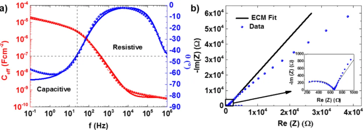
Figure 3.8– a) Schematic of the electrochemical cell setup with an area (A) of 1.039 cm2 and b) the
corresponding ECM suggested by Dasgupta et. al (adapted from[5]). ... 17
Figure 3.9 – a) The measured effective capacitance and phases (circles) and the ECM fited curves
(lines) and b) the respective nyquist plot of the lithium-based polymer electrolyte. ... 18 Figure 3.10– Cyclic voltammogram of stainless steel/electrolyte/stainless steel capacitor structure at a
scan rate of 10 mVs-1. ... 19 Figure 3.11 – a) The measured effective capacitance and phase (circles) and the ECM fited curves
(lines) and b) the respective nyquist plot of the paper. ... 20 Figure 3.12 - Schematic representation of the developed paper ZnO NPs FETs with an amplification of
the functionalized FSR top surface. ... 21
Figure 3.13 - Cyclic voltammogram of stainless steel/electrolyte plus ZnO NPs ink/stainless steel
capacitor structure at a scan rate of 10 mVs-1. The blue data plot represents the cyclic
voltammogram for the lithium-based polymer electrolyte and the black one represents the combination of the electrolyte with ZnO NPs ink annealed at 350 °C. ... 22
Figure 3.14 – IDS– VGS transfer characteristics, in saturation regime, as well the behaviour of IGS, for
three different annealing temperatures, namely 300, 350 and 450 °C of the ZnO NPs EGTs where ITO was selected for interdigital S/D electrodes. ... 24
Figure 3.15 – The total impedance |Z| variation with different frequencies of the screen-printed ZnO
NPs ink, with different annealing temperatures. ... 24
Figure 3.16 - IDS– VGS transfer characteristics for three different annealing temperatures, namely 300,
Field-Effect Transistors Based on Zinc Oxide Nanoparticles xiv
Figure 3.17–a) Cross-sectional schematic representation of the developed ZnO NPs EGT and b) an
image of the fully-printed ZnO NPs EGTs, on glass substrate. ... 26
Figure 3.18– IDS– VGS transfer characteristics, in saturation regime, as well as the behaviour of IGS, for
two different annealing temperatures, namely 300 and 400 °C of the ZnO NPs EGTs where carbon was selected for interdigital S/D electrodes. ... 27
Figure 3.19 - The drain current –drain voltage (IDS-VDS) output characteristics for both full-printed ZnO
NPs EGTs. ... 28
Figure 3.20 – IDS – VGS transfer characteristics, in saturation regime for two different annealing
temperatures, namely 300 and 400 °C of the ZnO NPs EGTs where carbon was selected for interdigital S/D electrodes. The double sweep measurements displays the hysteresis for both transistors as well as the influence of IGS. ... 29 Figure 3.21– The time response of the screen-printed ZnO NPs photodetector, after annealing at 300
°C, under OFF and ON UV light radiation. An image of the photodetector is displayed in the inset, where the black pattern corresponds to the screen-printed carbon interdigital S/D electrodes and the top coating (white) corresponds to the screen-printed ZnO NPs ink. ... 29
Figure 3.22– IDS– VGS transfer characteristics, in saturation regime, as well as the behaviour of IGS in
paper ZnO NPs FETs using to different W/L: 6.6 and 10.6, respectively. ... 30
Figure 3.23– IDS– VGS transfer characteristics, of the paper ZnO NPs FETs, in saturation regime using
to different W/L: 6.6 and 10.6, respectively. The double sweep measurements displays the large hysteresis for both transistors as well as the influence of IGS. ... 31 Figure 6.1– An example of the non-uniformity screen-printed electrolyte film, on glass substrate. .... 44
Figure 6.2 - TG-DSC curves of pure EC from Aldrich ... 44 Figure 6.3– ATR-FTIR spectrum of the compounds, in solution form except in the case of EC (powder),
used in the preparation of ZnO NPs ink. ... 45
Figure 6.4 - ATR-FTIR spectra of the ZnO NPs ink after being screen-printed and annealeted at different
temperatures from 24 to 450 °C. ... 45
Figure 6.5– The variation in cristallite size of the ZnO NPs with temperature. ... 46 Figure 6.6 - The topographical view, obtained by SEM, of the screen-printed vehicle on glass substrate.
... 46
Figure 6.7 –The XRD diffractogram of the EC powder and the ZnO NPs ink screen-printed on silicon
substrate and annealed at the inset listed temperatures. ... 47
Figure 6.8– The topographical view, obtained by SEM, of the top surface of FSR paper before being
functionalized with ZnO NPs. ... 47
Figure 6.9– Total impedance |Z| variation with different frequencies... 48 Figure 6.10 – Schematic representation of the charge mechanism in an electrolytic parallel plate
capacitor and the voltage profile plus the electric field distribuiton a) where no voltage is applied, b)
instantly after the voltage being applied, the dipolar relaxation, c) the ionic relaxation of the ions
leading to the EDL starting to build up, and d) the EDL formation at the
electrode/electrolyte/electrode interfaces. Adapted from [39]. ... 48
Figure 6.11– Magnification of the measured effective capacitance and phase (circles) and the ECM
fited curves (lines) for FSR paper ... 49
Figure 6.12 –a) Screen-printed ZnO NPs ink deposited on ITO interdigital S/D electrodes. The white
lines beneath the ZnO NPs film correspond to the patterned electrodes and b) shows an
amplification of the patterned electrodes. The table in c) shows the selected number of samples for
the determination of the channel length (L) for the L 200 ITO S/D interdigital electrodes. ... 49
Figure 6.13 - a) Screen-printed ZnO NPs ink deposited on carbon interdigital S/D electrodes. The light grey lines correspond to the pattern electrodes and b) shows an amplification of the patterned
carbon electrodes. The table in c) depicts the selected number of samples for the determination of
the channel length for the L 200 carbon S/D interdigital electrodes. ... 50
Figure 6.14– The time response of the screen-printed ZnO NPs ink, after annealing at 300 °C, as UV
Field-Effect Transistors Based on Zinc Oxide Nanoparticles xv
LIST OF TABLES
Table 1.1– Key parameters of the reported EGTs, where inorganic semiconductores were implemented,
i.e. the deposition technique, the temperature of the post-treatment, the used electrolyte, the voltage between drain and source (VDS), the threshold voltage (VTh), the On/Off ratio and the mobility (µ). 2 Table 3.1–Influence of the curing and annealing temperatures on the resisitivity of the carbon
screen-printed S/D electrodes. ... 21
Table 3.2–Average and standard deviation of the transistors’ layers thickness and W and L of the ITO
interdigital S/D electrodes... 23
Table 3.3– Summary of the electric characterization of the ZnO NPs EGTs with ITO as interdigital S/D
electrodes, annealed at 300, 350 and 450 °C. ... 25
Table 3.4 - Average and standard deviation of the transistors layers thickness and W and L of the carbon
interdigital S/D electrodes ... 27
Table 3.5 - Summary of the electrical characterization of the ZnO NPs EGTs with carbon as interdigital
S/D electrodes, annealed at 300, and 400 °C. ... 28
Table 3.6 - Summary of the electrical characterization of the paper ZnO NPs FETs with W/L of 6.6 and
10.6, respectively. ... 30
Table 6.1– Extracted parameters for the selected ECM with associated error to the determination of
CDL of the lithium-based polymer electrolyte. ... 48 Table 6.2– Extracted parameters for the selected ECM with associated error to the determination of
CDL of the Felix Schoeller raw paper. ... 49 Table 6.3– The selected number of samples for channel width (W) determination. ... 50 Table 6.4– The determined rise and fall time (𝜏𝑟 and 𝜏𝑓, respectively) by exponential fitting on the time
Field-Effect Transistors Based on Zinc Oxide Nanoparticles xvii
Motivation
Nowadays, printed electronics (PE) has become a hot-topic since there is a strong interest in replacing conventional silicon-based technology by simpler processing techniques in some low cost consumer electronics. Comparing the two technologies (conventional and PE) there are some clear advantages for the latter one, which are related to factors such as reduced fabrication costs associated to the manufacturing processes, the wasted material and benefits of the individual printing techniques (flexo, screen, rotary-screen, inkjet and off-set printing).[1] Out of these advantages other opportunities arise, such as the use of flexible substrates (e.g. polyethylene terephthalate (PET) or even paper) in order to design ultra-cost-effective, flexible, thin and environmentally friendly electronic devices. Additionally, they enable the production of large area printing on flexible substrates by roll-to-roll (R2R) processes, surpassing, in terms of throughput, the standard silicon wafer technologies available. Apart from that, printing techniques will reduce significantly the complexity of the manufacturing process, when lithography and etching steps are no longer necessary for circuit production.[2] Regarding the market needs, the IDTechEx Research predicts that for conductive inks and pastes a gross market revenue of $2.8 bn and $3 bn will be reached in 2020 and subsequently in 2025, respectively.[3]
Within this broad topic, the focus of this work is on the development of key electronic devices with low-cost materials (i.e. ink preparation for printing) at a laboratory scale, which could be compatible at an industrial scale in a R2R process. In this case, the emphasis will be on the semiconductor layer for field-effect transistors (FETs), in particular, the formulation of inks based on zinc oxide (ZnO) nanoparticles (NPs) dispersed into a cellulose matrix based on ethyl cellulose (EC), which will work as a thickening agent. Furthermore, oxide semiconductors have already shown outstanding performances in electronic applications.[4] Nevertheless, and regarding PE, organic semiconductors have been preferred since they can be easily processed into inks, particularly the polymers. Nonetheless, inorganic semiconductors can also be solution-processed but, in comparison to organic alternatives, high temperatures are fundamental, in order to remove binders or stabilizers. These so-called burn-out temperatures could compromise their application on flexible substrates.[5] Nevertheless, some communications have been made concerning inorganic semiconductors on electrolyte-gated transistors (EGTs) and many efforts have been made with the purpose to lower the working temperatures.[6][7]
Accordingly, it will be possible to build fully printed EGTs, using only screen-printing. These types of devices, apart from being printable, can operate at low voltages, owing to the high capacitance provided by the electrolyte’s electric double-layer capacitance (CDL), which works as the dielectric
layer.[8] However, due to the burn-out temperatures that are needed to degrade the binder, the intended EGTs will be built on glass substrates.
At the same time, paper electronics, has been undergoing a remarkable progress. Some of the most important benefits of paper are related to its low-cost and fast fabrication as well as its disposable and eco-friendly character.[9] Moreover, the potential of paper has been widely demonstrated in various applications such as a substrate for devices, sensors, solar cells, gas sensors and transistors, as well as an active part, more specifically as the dielectric layer in FETs, memories, and CMOS.[9]–[15]
Field-Effect Transistors Based on Zinc Oxide Nanoparticles xviii
Objectives
The main purpose of this dissertation is to design, fabricate and characterize field-effect transistors (FETs) combining cellulose with Zinc Oxide (ZnO) nanoparticles (NPs). The focus will be on the development of printed electrolyte-gated transistors (EGTs) where the ZnO NPs will be used as the semiconductor material in a staggered top-gate architecture, with interdigital indium tin oxide (ITO) or conductive carbon as source and drain contacts and silver as gate electrodes.
In parallel, the possibility to coat conventional paper with ZnO nanoparticles by sol-gel method in aqueous medium of zinc acetate dihydrate (ZnC4H6O4·2H2O) and sodium hydroxide (NaOH) will also
be demonstrated. Consequently, it shall be possible to build a FET, where paper can be used not only as a substrate, but also as the dielectric and the semiconductor, after functionalizing the cellulose fibers on one side of the paper with ZnO NPs. Here a staggered bottom-gate architecture will be adopted, where source, drain and gate electrodes will be deposited by physical vapour deposition (PVD) techniques.
Therefore, for a better understanding, the main following objectives will be covered:
Characterization of the properties of ZnO nanoparticle films deposited by screen printing technique and sol-gel method;
Study of the influence of temperature on the degradation of EC, working as a sacrificial binder of ZnO screen-printed films.
Study of Electrochemical Impedance Spectroscopy (EIS) of the lithium - based polymer electrolyte and paper, for ZnO NPs EGTs and paper ZnO NPs FETs respectively;
EIS characterization of the ZnO screen-printed films;
Electrical characterization of the interdigital contact electrode materials for EGTs;
Field-Effect Transistors Based on Zinc Oxide Nanoparticles 1
1. INTRODUCTION
Recent developments over the last decade on the field of nanostructured zinc oxide (ZnO) surfaces and nanoparticles (NPs) opened the way for application in several areas, ranging from thin-film transistors (TFT)[16]–[18], dye-sensitized solar cells[19], piezoelectric devices[20], gas sensors [21], opto- and microelectronics[22] to biomedical applications, such as antibacterial and antifungal agents in medicine[23]. Figure 1.1 exemplifies the implementation of ZnO nanostructures in some of such devices.
Figure 1.1– Three applications of ZnO nanostructures a) as an UV photodetector[24], b) as an anti-bacterial
agent[25] and c) as a flexible nanogenerator (FNG).[26]
The inherent electrical properties of ZnO make it a well-established candidate for its subsequent integration into semiconducting devices, such as transistors. The following sections will give a brief introduction to ZnO nanostructures, as well to transistor technologies and the concept used in this work of electrolyte-gated transistors (EGTs) and its advantages, especially in the context of printed electronics (PE).
1.1. Zinc oxide: Main features, structures and its application in electronics
Over the last decades, interest in the synthesis and application of nanoscale materials has been growing, due to their unique mechanical, electrical, optical and chemical properties that are different from the bulk, particularly, due to high surface-to-volume ratio and spatial confinement. This brings new approaches in the field of electronic devices. In this specific area the transistor (characterized as an electric On-Off switch) is one of the most crucial semiconducting electronic components in nowadays technologies.[27] The focus for these devices is on the improvement of their performance, which is closely relate to the semiconductor capability of free charge carrier accumulation in the transistor channel at the semiconductor/dielectric interface.[28]
In this context, ZnO is characterized as an excellent inorganic n-type semiconductor material, which has a direct bandgap of 3.37 eV and a free-exciton binding energy of 60 meV at room temperature, where the most common crystalline phase is of hexagonal wurtzite nature.[16] Various methods of synthesis, such as chemical vapour deposition (CVD)[29], hydrothermal methods[24][19] or via sol-gel method[30] have been reported in the way to tailor a wide range of ZnO nanostructures, such as nanoparticles, nanorods, nanowires or thin films. Different shapes, sizes and morphologies determine the chemical and physical properties of the ZnO, as well as the corresponding electrical, optical and piezoelectric ones.[24] Also its long durability, heat resistance (melting point 1975 °C) are preceded over organic semiconductor alternatives.[28]
Field-Effect Transistors Based on Zinc Oxide Nanoparticles 2
the same table, different techniques such as printing have been employed for EGTs fabrication, but to our knowledge, always at least one of the layers has not been printed. Consequently, the main goal of this work is to achieve fully-printed inorganic EGTs.
Table 1.1– Key parameters of the reported EGTs, where inorganic semiconductores were implemented, i.e. the deposition technique, the temperature of the post-treatment, the used electrolyte, the voltage between
drain and source (VDS), the threshold voltage (VTh), the On/Off ratio and the mobility (µ).
Semiconductor Deposition
technique
Post-treatment Electrolyte
VDS
(V) VTh (V) On/Off
µ (cm2 (Vs)-1)
ZnO [32] Spin-coating 280 ºC Ion Gel 0.7 1.16 2.64x10⁵ 12.1
In2O3[33] Inkjet - PVA+KF 0.4 0.54 2x10³ 0.8-0.26
ITO[5] Inkjet 400 ºC CSPE 0.8 - 0.22 2 x 10⁴ 5
ZnO [34] Aerosol Jet Printing 250ºC Ion Gel 0.1 0.97 2.15x10⁵ 1.67
GIZO[7] Spin-coating 250 ºC CSPE 1 1.9 1x10⁵ 1
IGZO[35] Spin-coating 350 ºC KCl 0.5 0.16 1.4x10⁷ 10.82
Since ZnO can be processed and printed, using solution precursors, ZnO obtained from sol-gel method[30] and commercial ZnO nanoparticles (NPs) will be explored in ways to work as the semiconductor layer in FETs and EGTs, respectively. In the next subsection, the mode of operation of these two types of devices will be briefly explained.
1.2. Transistor technologies and electrolyte-gated transistors
Since the development of the first transistor by John Bardeen and Walter Brattain, the information technology has been revolutionized.[36] Particularly, FET has become one of the most implemented semiconductor devices. The fundamental characteristic of these devices is the modulation of a current between two electrodes (source and drain, IDS) with a voltage applied at a third electrode
(gate, VGS). The term field-effect derives from the fact that an electric field, generated by the application
of VGS, develops throughout the channel region, capable of inducing (accumulating) charge carriers in
the channel, which can be collected by the drain electrode (in the case of an n-type FET). The field-effect mode has been harvested for many microelectronic applications and culminated in cutting edge technologies like the metal-oxide-semiconductor field-effect transistor (MOSFET)[37] or the thin-film transistor (TFT).[38] Whereas MOSFETs rely on diffusion/implantation processes into crystalline silicon substrates (wafers) [27] TFTs are fabricated using layer-by-layer deposition techniques. The interest into TFTs was governed mostly by the need for higher substrate varieties and fabrication in large areas, resulting in modern application fields such as displays, paper and flexible electronics.[4][10][11]
The use of electrolytes instead of a conventional dielectric layer in a FET results in an EGT.
One of the key features aimed for an electrolyte is the low electrical but high ionic conductivity (σ and σi, respectively). This allows the electrolyte to behave as a pseudo dielectric, bridging the gap between
a conductive gate electrode and the channel region. By applying a VGS ions migrate in the electrolyte,
in this case in the composite solid polymer electrolyte (CSPE), accumulating at the respective interfaces, forming electric double-layers (EDLs) as illustrated in Figure 1.2 a). The electric field at these EDLs becomes very high and is capable of effectively inducing charges into the semiconductor.[39] This effect can be used for transistor applications,[8] to investigate insulator-to-metal transitions[40] or superconductivity behaviour of insulators.[41]
The evolution from conventional dielectric materials (oxides and nitrates) to electrolytes was governed by the need for higher transistor driving currents, since it is directly proportional to the capacitance of the dielectric layer per unit area (Ci), as we can see in equation 1.1:
𝐼𝐷=𝑊𝜇𝐹𝐸𝐿 𝐶𝑖[(𝑉𝐺− 𝑉𝑇)𝑉𝐷−𝑉𝐷 2
Field-Effect Transistors Based on Zinc Oxide Nanoparticles 3
where W and L are the channel width and length, respectively, and µFE the field effect mobility.
Electrolytes are capable of reaching values in the order of 1 –10 μFcm-2, outperforming even high-k
dielectrics[42]–[44], consequently their integration into semiconductor devices became straightforward. EGT applications range from textile fibers, biosensors, supercapacitors or electrochromic displays.[8] High capacitance dielectrics also enable the EGTs to operate at reduced voltages, advantageous for low power dissipation devices.[34] Furthermore, the inherent properties of electrolytes as gates offer not only exceptionally low source and drain contact resistances,[45] still presenting a downside in conventional transistors, but also new possibilities in PE devices, owing to the solution processability of many solid electrolytes.[46]–[48]
A considerable drawback to employ EGTs remains in their significant gate leakage currents (IGS), arising from considerable charging currents of the ion accumulation process.[8]Consequently, the
decision to employ EGTs will depend on understanding which figure of merit is most crucial for a given application.[49] As well, the ionic conductivity of the electrolyte is crucial for the intended application since the ionic charge motion, in the electrolyte, depends on the diffusion and the migration, owing to the concentration gradient and the electric field, respectively. The nature of the electrolyte either liquid, solid or gel, is also significant for the ion motion process.[39] As a result, the time response of the EGTs will depend the ionic conductivity and the interaction with the semiconductor layer.[50]
For this work, EGTs as depicted in Figure 1.2 b) were the most suitable solution as the aim was
the fabrication and characterization of fully printed FETs.
Figure 1.2–a) Cross-section schematic representation of the staggered top-gate structure with interdigital source and drain contacts adopted for the fully printed ZnO NPs EGTs on glass substrate. The respective
EDL formations at each interface is also illustrated. b) A 3D schematic representation, where bottom black
and top silver layers are the source/drain and gate electrodes, respectively. Whereas the white and the yellow layers represent the ZnO NPs and the composite solid polymer electrolyte (CSPE) film, respectively.
Since printing was selected as the deposition technique for device fabrication in this work, the next section will introduce some fundamentals about PE and highlight advantages and disadvantages of the processes involved.
1.3. Printed electronics and printing techniques
Printing processes have developed/adapted with the progress in electronic manufacturing technology and it is prominent that a large potential can be provided, by combining this technology with the notorious advances in nanomaterials for electronic applications. These continuous demands for new materials, new methods or techniques, make PE, the key technology for designing ultra-cost-effective, as well as flexible, thin, low power consuming, and environmentally friendly electronic devices. Some of them are already known as large area printed pressure sensors[51]–[53], organic light emitting devices (OLED)[54]–[56] or solar cells.[57]
Field-Effect Transistors Based on Zinc Oxide Nanoparticles 4
intended application, depends on a number of properties, including the required printing quality, the substrates, the inks and especially the resolution.
Printing techniques offer a variability of benefits against photolithography and vacuum processes since they are fast, low-cost, offer fast prototyping, allow the reduction in material waste and they enable the production of large area printing on flexible substrates by roll-to-roll (R2R) processes. [58][59] Nevertheless, the resolution limits of the current printing techniques have an effect on the performance of printed devices. In addition, as all printable materials are in solution form, their physical and chemical stability, as well as viscosity, compatibility of the solvents and surface energies are the major paradigms in choosing the suitable printing technique and evidently in the devices final performance.[54][56]–[58]
It is desired to fabricate fully functional devices, using solely one printing technique instead of a combination of the ones mentioned above, as this facilitates the fabrication process, leading to a more cost-effective production. This approach was shown in recent scientific publications in a wide range of applications: as patterning source and drain electrodes[62], or for all-printing stretchable electrochemical devices.[63]
Therefore, in this thesis, screen-printing was chosen as the only fabrication technique to produce the EGTs. Owing to the printed circuit board industry, it is the most versatile printing technique and a quite mature technology for PE, in comparison to the ones mentioned before.[2] High aspect ratio of printed objects is the most distinct feature of this technique. In addition, a wide range of thicknesses, reaching from a few µm up to 100 µm can be achieved, which cannot be obtained by other printing techniques.[64]
This technique is based on a screen mesh, which may be polyester or stainless steel, with a defined printing pattern. This pattern is defined by photolithography of a light sensitive emulsion on the mesh. A squeegee, of rubber or metal, moving over the screen, provides shear stress to the ink (or printable paste), consequently decreasing its viscosity (viscoelasticity) and allowing it to cross through the open areas onto the substrate. Solution viscosity, printing speed, angle and geometry of the squeegee, mesh size, material, strength and snap-off (distance between screen and substrate) are the main factors to consider in order to achieve high-resolution patterning (30 - 50 µm), through this printing technique.[64] Viscosities, typically between 500 - 5000 cPs are referred to as desirable for this technique, since inks with low viscosity will run through the mesh rather than dispensing out of it.[64] As well, to obtain a high-resolution line width a compromise between surface energies, either of the substrate or the ink, is required. Low surface energies of the substrate provides reduction of the wettability of the printable paste, which leads to improved line resolutions. Moreover, as we can change the wettability of the substrate, by controlling its surface energy, low viscosity inks can also be used to achieve good resolutions.[60] A schematic drawing of the used screen-printing system, present in CENIMAT|i3N, is displayed in Figure 1.3.
Field-Effect Transistors Based on Zinc Oxide Nanoparticles 5
Considering the required ink properties and their influence on the used printing technique the next subsection will give a short overview of the ink preparation as well as some crucial remarks on its composition.
1.3.1. Ink formulation and properties for thick films
The synthesis of a nanoparticle thick-film (thicknesses in micro scale) ink must be made by a careful selection of the raw materials, so that its characteristics do not compromise the intended application. The ink must be prepared dispersing the desired inorganic powders/precursors in a viscous liquid, the vehicle, which is responsible for the deposition of the powder onto the substrate. Both of these components must be dispersed along with an organic or sacrificial binder with a solvent and a wetting agent. For this, resin or polymeric binders such as cellulosic polymers, as is the case of ethyl cellulose (EC) is widely used for industrial screen-printing as it provides good printing and levelling.[66] The sacrificial binder is used in order to hold the inorganic powders together and give the ink the intended rheological properties.[67] Additionally, solvents with low vapour pressure at room temperature and a high vapour pressure at 100 – 150 °C, should be selected, in order to prevent ink drying by evaporation on the screen and enable rapid drying of the printed parts by annealing.
Thereby, to obtain the mechanical and electrical required properties, which are given by the powder, the vehicle must be eliminated (“burned-out”), so there will be no trace of it in the final film. Nevertheless, the properties of the thick-film are not just influenced by the bulk properties of the inorganic powders, but also by their surface area, particle size, tap density, purity and interface quality. For instance, surface area influence viscosity, particle size and their dispersion effect, which in turn has an effect on ink behaviour, film surface smoothness, film conductivity, film density, printing and its adhesion to the substrate.[68] Due to the presence of agglomerates, large interface roughness between the transistor channel and the gate insulator can occur, forming charge traps, which makes the charge transfer between source and drain electrodes difficult. Consequently, the turn-on voltage (VOn) and the
subthreshold swing (Ss) of the devices can be impaired. One way of overcoming this problem is to
stabilize the nanodispersions with surfactants.[5] However, the presence of the vehicle, as well as surfactants or additives decline the electrical performance of the thick-film, likewise the type of substrate that can be used, since high temperatures or UV irradiation is needed to burn them out.[5][65]
1.4. Inorganic field-effect transistors on paper
Paper electronics appears as a new area of technology, which has begun to show that it is possible to counteract all the issues related to a decrease in waste material, making technology cheaper, disposable and eco-friendly, even if this new approach is on an early stage of development. Furthermore, paper is also recyclable, lightweight and widely used as a flexible substrate in everyday life. Additionally and most importantly manufacturing process can exceed 100 kmh-1, making it cheap (≈
0.1 cent dm-2) compared to other substrates used in electronics, like for instance polyethylene terephthalate (PET ≈ 2 cent dm-2).[9]
The first step in the application of paper as a substrate in electronics, was given in 1968[31], having today several applications of it as substrate for sensors, solar cells, gas sensors or displays. Nonetheless, many efforts have been made to make it more functional beyond a simple substrate.[69] Fortunato et al. have shown for the first time (see Figure 1.4 a)), using this remarkable material, that in
addition to the substrate, it can also work as an active part i.e. dielectric in FETs.[11] The benefit of being applied as dielectric is related to its foam-like structure that enables moisture retention, which produces a large gate capacitance at low frequencies due to the free charges.[70]
This technological leap made their application in memory transistors[14] and CMOS devices[15] possible. Recent studies also confirm that the properties of the paper-based transistors are affected by the structure, fiber type and thickness of the paper.[12][13]
Field-Effect Transistors Based on Zinc Oxide Nanoparticles 6
it will be possible to coat the cellulose fibers of the paper substrate with ZnO nanoparticles under ambient atmosphere at room temperature. Thus, to build an interstate structure (similar to the one in Figure 1.4 b)), where this time paper can play three different roles: substrate, dielectric and semiconductor after being functionalized, is feasible.
Figure 1.4–a) An image of the developed FETs in CENIMAT|i3N where paper was applied as substrate and
Field-Effect Transistors Based on Zinc Oxide Nanoparticles 7
2. MATERIALS AND METHODS: FABRICATION, OPTIMIZATION AND
CHARACTERIZATION PROCESS OF EGTs and FETs
This chapter aims to present all the steps that were taken for the production and characterization of EGTs on glass and FETs on paper. First, the formulation of the semiconductor layer will be presented, which in case of EGTs is a printable paste, containing a dispersion of ZnO nanoparticles in a sacrificial binder EC. In case of the paper ZnO NPs FETs, paper was coated with ZnO NPs by sol-gel method, in an aqueous solution of zinc acetate dihydrate and sodium hydroxide.
Secondly, the architecture chosen for each transistor type will be displayed as well as the steps and techniques that were used for all the layer depositions.
Finally, all the characterization techniques selected to study the morphology, structure and stability of the semiconductor and electrolyte layers will be listed. In the end it will be shown how the electrical characterization of the final devices was conducted.
2.1. ZnO NPs ink formulation materials and reagents
The methods used for preparing ZnO NPs screen-printing paste were based and adapted from the literature.[71] First, the vehicle was prepared by dissolving 5 %wt Ethyl Cellulose 300 cP (C6H7O2
(OC2H5)3; CAS: 9004-57-3) from Aldrich on an 80:20 toluene/ethanol solution (C6H5CH3; CAS:
108-88-3/ C2H6O; CAS: 64-17-5). After complete dissolution, which takes around 12 hours under stirring at 600
rpm, 0.25, 0.5, 0.75 and 1 g of ZnO nanopowder, <100 nm particle size (CAS: 1314-13-2) from Aldrich were added always in the same amount of vehicle. The solutions should be kept under continuous stirring until their complete dispersion.
2.2. ZnO semiconductor layer by sol-gel method
As mentioned in section 1.4 and taking into account the work done by Jaber and Laânab[30] a piece of Felix Schoeller raw (FSR) paper, was submersed in an aqueous solution. For that, 4 cm2 of
FSR, which consist of pressed cellulose fibers with high porosity and 141 µm of thickness, obtained from Felix Schoeller with, was covered on one side by adhesive kapton tape. The solution was prepared by mixing 1.757 g of zinc acetate dihydrate (CAS : 5970-45-6, ZnC4H6O4·2H2O, MW: 219.51) from
Sigma-Aldrich and 0.796 g sodium hydroxide (NaOH), previously dissolved in 100 ml and 20 ml of deionized water, respectively. Firstly, the paper must be immersed in the zinc acetate solution and then NaOH at a rate of 2 ml/min was added. While adding NaOH, the stirring should increase to 1300 rpm and be maintained for 1h. Finally, the paper was washed with deionized water to remove excess and left drying in air. It is necessary to supervise the process because the paper can glue up the edges of the beaker and can get stuck due to the stirrer.
2.3. Fabrication and optimization of the ZnO NPs EGTs and paper ZnO NPs FETs
2.3.1. ZnO NPs EGTs by screen-printing
Field-Effect Transistors Based on Zinc Oxide Nanoparticles 8 Figure 2.1– Schematic representation of the ITO interdigital S/D electrodes patterned via photolithography.
Figure 2.2– Schematic representation of the developed fully-printed ZnO NPs EGTs.
2.3.2. Paper ZnO NPs FETs
As mentioned in 2.2 the first step consisted in growing ZnO nanoparticles on the cellulose fibers on the surface of FSR paper, which was itself used as a dielectric for the intended devices. Figure 2.3 displays a simple schematic representation, of the steps that were taken in order to achieve a staggered bottom-gate architecture, for the paper ZnO NPs FETs. Nevertheless, in Annex A a more detailed description of the whole fabrication is shown.
Figure 2.3 - Schematic representation of the developed paper ZnO NPs FETs.
2.4. Characterization techniques
Several techniques were used in order to characterize the various layers of the transistors. The rheological behaviour of the ZnO ink and the lithium-based polymer electrolyte was evaluated using Bohlin Gemini HRNANO rotational rheometer, with parallel plates geometry (20 mm diameter and 500 µm
Field-Effect Transistors Based on Zinc Oxide Nanoparticles 9
30 s, followed by an equilibration time of 180 s. A solvent trap was used in order to avoid evaporation. The steady-state measurements were performed for shear rates up to 1000 s−1
.
Atomic force microscopy (AFM) was performed in non-contact mode using an Asylum MFP-3D
instrument. The resolution of the image was 512 lines by 512 columns and the scan size was 5×5 μm2
and 20×20 µm2.
Both semiconductor layers were characterized by SEM-FIB using a Carl Zeiss AURIGA CrossBeam workstation instrument. As well as the crystallinity and structure of the samples were obtained by X-Ray Diffraction (XRD, PANalytical, model X’Pert Pro), in Bragg-Brentano geometry with
Cu Kα line radiation (λ=1.5406 Å) at 45 KV and 40 mA. Particularly, in the case of ZnO screen-printed films XRD analysis was performed first at 30 °C and subsequently between 100 °C and 500 °C, with a step of 50 °C.
Fourier transform Infrared (FTIR) spectroscopy was applied in order to evaluate the EC, toluene and ethanol thermal degradation. The ZnO ink was screen-printed on glass substrates, previously cleaned in acetone, IPA and DI water and then exposed to different annealing temperatures, ranging from 100 °C to 450 °C, with a step of 50 °C, on a hotplate. The spectra were acquired between 4500-500 cm-1 by a Nicolet 6700 FTIR Thermo Electron Corporation device. In addition, with the same
purpose of understanding the thermal degradation of the ink constituents, thermogravimetric and differential scanning calorimetry (TG-DSC) measurements were carried out on the semiconductor ink solution with a Simultaneous Thermal Analyzer (TG-DSC - STA 449 F3 Jupiter). Approximately 20 mg of each sample was loaded into an open Al crucible and heated from room temperature to 550 °C with a heating rate of 5 °Cmin-1, in ambient conditions.
Electrochemical Impedance Spectroscopy (EIS) was done using Gamry Instruments Reference 600 Potentiostat in order to determine:
The capacitance-frequency dependency of the lithium-based polymer electrolyte samples inserted between stainless steel discs with an area of 1.039 cm2 (see Figure 3.8 a)). The results
were acquired in a frequency range of 1 MHz to 100 mHz with 25 mV as ac excitation voltage at 1 V dc.
The capacitance-frequency dependency of FSR paper, using gold discs with an area of 1.77 cm2 and in a frequency range of 1 MHz to 10 mHz with 5 mV as ac excitation voltage.
Previously, both sides of the paper were coated with about 120 nm of aluminium by e-beam evaporation, in order to improve the electrical contact between the paper and the gold discs.
The impedance spectroscopy of the ZnO thick films was evaluated in a frequency range of 1 MHz to 10 mHz with 25 mV as ac excitation voltage. For that, step number 2 and 3 of the Annex A were followed, but a wider range of temperatures was established, including room temperature, 100 °C and from 200 to 400 °C, with a step size of 50 °C.
The electrochemical response of lithium-based polymer electrolyte and the combination with annealed ZnO ink was evaluated by cyclic voltammetry (CV) through a Gamry Instruments Reference 600 Potentiostat. Doctor blade technique was used in order to deposit both layers, on stainless steel discs. In the case of the electrolyte, the layer was exposed, first to UV radiation during 5 min and, afterwards, dried on a hotplate at 70 °C. On the other hand, the ZnO thick-film was annealed, during 30 min at 350 °C. All films were electrochemically cycled from 4 to -4 V, at a scan rate of 10 mVs-1.
Furthermore, the Olympus BX51 microscope, and the software Cell A were used to measure the transistors’ dimensions. In particular, the semiconductor channel lengths and widths were measured using a Leica IC80 HD microscope and the LAS V4.3 software.
Electrical measurements of the resistivity of carbon and silver electrodes were performed using the four-point probe technique (Jandel Enginneering Ltd) and the thickness of the screen-printed films were measured with an Ambios XP-Plus 200 Stylus profilometer.
Field-Effect Transistors Based on Zinc Oxide Nanoparticles 11
3. RESULTS AND DISCUSSION
3.1. Characterization and properties of ZnO NPs ink semiconducting layer
In this section, the focus will be on the development and characterization of both of the semiconductor and the electrolyte layers. As was already mentioned before, screen-printing depends highly on the used inks and their non-newtonian behaviour during the deposition process. Consequently, rheological measurements were performed on the used functional inks (ZnO and electrolyte).
After verifying a good dispersion of the powder and the viscous character of the solutions listed in section 2.1, thick films of ZnO NPs were printed on glass substrates, using a mesh model 77-55 (mesh count 190,aperture 81 µm thread diameter 55 µm).
After visual and microscope inspection, the solution with 1 g of ZnO powder resulted in best uniformity, compactness and adhesion, where films with an average thickness of 1.39 µm were achieved. Therefore, this was the ink employed and characterized as the semiconducting layer.
After deposition, the vehicle’s response to high temperature during the burn-out process will be investigated by TG-DSC, as this determines the necessary temperature at which the film should be subjected in order to retain solely its semiconductor content. The films will then go through a number of characterization steps to further investigate their structural and morphological properties (FTIR, SEM, and XRD) in respect to the applied annealing temperatures.
3.1.1. Rheological measurements
The rheology of the ink is strongly dependent on the rheology of the vehicle since sacrificial binder and solvent are the main components for screen-printing inks. It is also pertinent to preserve good printability during the time it remains on the screen and the printing parameters must allow for high yield. Thus, the variation of the steady-state viscosity as a function of the shear rate was performed for ZnO NPs ink, vehicle and lithium-based polymer electrolyte, as shown in Figure 3.1.
Figure 3.1– Viscosity as function of the sear rate for ZnO NPs Ink, vehicle (EC 5 wt% on toluene/ethanol)
and lithium- based polymer electrolyte.
First, a decrease of the viscosity with increasing shear rate is noted, especially for vehicle and electrolyte, which is related with their viscoelastic properties, allowing them to cross through the screen open areas onto the substrate.
In the case of ZnO NPs ink it is possible to say the viscosity is practically independent of the shear rate applied. Furthermore, the addition of ZnO nanoparticles decreases the viscosity of the vehicle, particularly of the EC since it is a polymer working as a sacrificial binder. This fact is expected as a result of the presence of nanostructures inside a polymer nanocomposite (PNC), which can modify its structural, dynamical and viscous behaviour. These changes are arising not only from the high surface-area-to-volume ratio of the nanoparticles but also due to the strong polymer-nanoparticles
0.1 1 10 100 1000
102 103 104 105 106
ZnO NPs Ink Vehicle
Electrolyte
Shear Rate (s-1)
Viscosity (
Field-Effect Transistors Based on Zinc Oxide Nanoparticles 12
interactions, which affect the entanglement of the EC chains.[72] Also, It is possible to affirm that ZnO NPs ink shows a newtonian flow for the applied shear rate range, since there is no significant change in its viscosity during the measurement, except for 100 s-1, where only a slight change was verified. This
indicates that the printed semiconducting films are less affected by printing parameters such as the applied force or velocity during the deposition. Consequently, reproduction of the films are favoured even when altering the deposition parameters, which happens when doing it by hand in a non-automated way. Nevertheless, it is necessary to take heed, since inks with low viscosities can pass through the mesh without the application of any shear stress. Furthermore, the formulated semiconducting ink shows good printability, good adhesion to the glass substrate and high uniformity which are crucial properties for instance for high interface quality and improved yield of the final EGT devices. Additionally, the ink was easily removed from the screen during the clean-up process with EtOH, which is desirable especially on an industrial scale with online R2R processes.
In contrast, the electrolyte exhibits mostly a non-newtonian behaviour. Furthermore, the fact that its dynamic viscosity is high becomes a problem when printed through the mesh, since the ink is blocked and it gets difficult to obtain a uniform printing pattern. This resulted in non-uniform films with defects, affecting the semiconductors coverage and consequently the performance of the devices. An illustration of the screen-printed electrolyte film on glass substrate can be accessed in Annex B. It might suggests that in order to achieve an improved printed layer a better control under the applied shear rate should be done. Through the homemade screen-printing it could be quite challenging; however, via an automatic one a better understanding of the phenomenon might be possible. As a result, snap-off, shear rate, angle, geometry and squeegee type could be investigated in the printed layers reproducibility.
3.1.2. TG-DSC of the vehicle and ZnO NPs ink
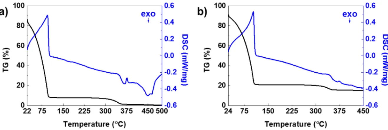
Via Thermogravimetric-Differential Scanning Calorimetry (TG-DSC), it was possible to evaluate the thermal behaviour of the vehicle, specifically to quantify the range of temperatures needed to burn it out. The TG-DSC measurements were performed from room temperature to 550 °C; here however only temperatures at which important endothermic reactions were detected will be shown and discussed. The TG-DSC results of the vehicle are represented in Figure 3.2 a), where a maximum peak of 0.48 mWmg-1 is observed for 93.9 °C. This peak is associated to an endothermic reaction, which
represents the evaporation of the organic solvents. Simultaneously to this reaction, a significant mass loss is observed, further confirming the evaporation of the solvents i.e. toluene and ethanol, since their boiling points are 78 °C and 110.6 °C, respectively. In addition, for temperatures above 350 °C, there is
almost no mass loss, which suggests that EC was fully degraded, which started to occur gradually above about 270 °C, as shown in Annex C.[73]
Figure 3.2–TG-DSC curves of a) vehicle solution (EC 5 wt% on Toluene/ EtOH and b) ZnO NPs ink.
Field-Effect Transistors Based on Zinc Oxide Nanoparticles 13
room temperature, which is associated to the low flash points of both solvents, 12 and 14 °C for ethanol and toluene, respectively. Once again, for temperatures above 270 °C degradation of EC, owing to the
associated mass loss, is suggested. On the other hand, above 400 °C, there still is ZnO powder present
in the crucible, since TG-DSC data still shows a linear positive mass value. This is not the case for the pure vehicle solution, reaching 0 % of initial mass for the final temperature. This observation indicates a 100 % thermal degradation of the vehicle; the desired effect of the burn-out process. Combining the knowledge of the individual measurements leads to the assumption that an annealing step above 300 ºC of a screen-printed ZnO NPs thick film would lead to a pure ZnO NPs film, which can then be used as the functional semiconducting layer in an EGT.
The next subsection will focus on the burn out process but this time on ZnO NPs ink screen-printed on glass substrates. The idea is to verify through the Attenuated Total Reflectance-Fourier Transform Infrared Spectroscopy (ATR-FTIR), if thick films exhibit the same behaviour in relation to the increase in temperature, as in the previous subsection concerning their ink form.
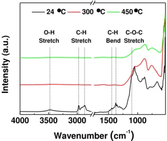
3.1.3. ATR-FTIR of the ZnO NPs ink
The study of the thermal decomposition of the vehicle, namely the EC content was studied also by ATR-FTIR. The semiconductor ink was screen-printed on glass substrates and annealed at different temperatures. In Annex DAnnex an ATR-FTIR spectrum of the compounds in solution form is also shown. Figure 3.3 shows the FTIR spectra for 24 °C, 300 °C and 450 °C. For EC, the peak at 3500 cm- 1
represents the stretching of O-H groups both in the closed ring structure and in intra/intermolecular hydrogen bonds. The peaks around 2980-2870 cm-1 may indicate CH stretching and the distinct peak
at 1375 cm-1 refers to CH3 bending. Additionally, the small peak at 1440 cm-1 represents CH2 bending,
and the broad peak around 1100 cm-1 may be due to C-O-C stretching in the cyclic ether.[74]
Figure 3.3 - ATR-FTIR spectra of the ZnO NPs ink after being screen-printed and annealeted at 24, 300 and 450 °C.
Annex E provides a better understanding of the temperature effect on the screen-printed films. At 100 °C, there are signs of thermal degradation of the ink, since there is a decrease of the absorbance peaks, however quite small. The spectra for 150 °C and 200 °C remain virtually the same, though, the spectrum for 250 °C shows a clear reduction of the absorbance peaks mentioned above, indicating the beginning of EC thermal decomposition. The absorbance peaks for EC have almost disappeared for 300 °C and finally, from 350 °C to 450 °C, there are no absorbance peaks corresponding to EC, meaning that the polymer has been degraded.
In addition to this, a notable loss of adhesion of the films to the substrates was identified after annealing, especially for those with annealing temperatures above 300 °C. This detail is expected since EC works as a binder (improves adhesion), which is lost after application of the burn-out temperatures
4000 3500 3000 1500 1000
C-O-C Stretch C-H
Bend
C-H
Stretch
24 C 300 C 450 C
![Figure 1.1 – Three applications of ZnO nanostructures a) as an UV photodetector[24], b) as an anti-bacterial agent[25] and c) as a flexible nanogenerator (FNG).[26]](https://thumb-eu.123doks.com/thumbv2/123dok_br/16692394.743697/23.892.137.784.293.474/figure-applications-nanostructures-photodetector-bacterial-agent-flexible-nanogenerator.webp)