Effect of High-k Oxide on Double Gate Transistor Embedded in RF Colpitts Oscillator
M. Bella
1, S. Latreche
1, C. Gontrand
21 Université frères Mentouri Constantine, Laboratoire d’Hyperfréquence et Semi-Conducteurs, Département d’Electronique Constantine, Algeria
2 Institut de Nanotechnologies de Lyon (INL), University Lyon1, Lyon, France
(Received 15 June 2016; published online 29 November 2016)
This paper present a comprehensive analysis of LC Colpitts Oscillator built around a DGMOS (Double Gate Metal Oxide Semiconductor) transistor using high-k technology. A mixed- mode simulation is in-volved, applying a quantum model to the device whereas the rest of the considered circuit is governed by
Kirchhoff‟s laws. The quantum device model correspond to 2D numerical calculations based on self-
con-sistent codes coupling Poisson and Schrödinger equation along the transport direction, considering an e f-fective mass approximation. A comparison with Drift Diffusion model (DDM) is made in order to point out importance of quantum effect in this nanometer device. The impact of high-k oxide gate is investigated and analyzed; the results confirm that the high-k is an interesting alternative to reduce tunneling gate current of the DGMOS transistor but reach the same drain one. Considering the oscillator, our goal is focused on the analysis of its phase noise.
The Linear Time Variant (LTV) model of phase noise is considered. It is based on the Impulse Sensi-tivity Function (ISF) which describes carefully the sensiSensi-tivity of an oscillator to a parasite impulse current injection in different nodes of the circuit. The obtained results pointed out that the ISF function is sinus-oidal and its period is nearly the same of the oscillator output signal for different dielectric oxide. It also states that the phase noise of a Colpitts oscillator is not affected by the use of the high-k materials. Finally this method, if extended, is a good tool to investigate a perturbation response on such circuits.
Keywords: DGMOS transistor, Radio-frequency, Mixed-mode simulation, Phase noise ISF funcfion.
DOI: 10.21272/jnep.8(4(1)).04022 PACS numbers: 85.30.Pq, 85.30.Tv
1. INTRODUCTION
Double Gate Silicon-on- Insulator (DG SOI) devices have been of great interest, particularly for the investi-gation of sub-10 nm field-effect transistor [1]. They seem to be promising candidates thanks to their excel-lent SCEs (Short Channel Effects) minimization: higher drive current and transconductance, lower leakage cur-rent, better DIBL (Drain Induced Barrier Lowering) and better scaling capability compared to the bulk MOSFETs [2-4].
To continue the downward scaling, gate oxide with higher dielectric constant is considered as a solution to achieve an interesting transistor performances while maintaining a relatively thick physical thickness of the oxide in order to minimize the leakage tunnelling cur-rent. Many research works have been performed in this area [5, 6]. Hafnium oxide (HfO2) and Zirconium oxide (ZrO2) are considered for present and future CMOS application [5, 7]. On an other hand, high-speed silicon based technologies have emerged as attractive candi-dates for low – cost systems in Radio Frequency (RF) wireless communications.
Phase noise in RF oscillators is an important item in the design of integrated transceivers [8, 9]. As a result, different phase noise theories have emerged. Several papers addressing phase noise have been published [10-14]. Indeed, Hajimiri and Lee [11] have proposed a time variant model (LTV) based on the so-called Im-pulse Sensitivity Function (ISF) to predict phase noise. This technique provides insight into the design of oscil-lator. The ISF function characterizes the stationary results of a perturbation.
Two types of simulation tools have been developed
for this work. The first tool which can be applied to design nanoscale transistor, requires accurate quantum transport physics. This model corresponds to a self-consistent pseudo 2D solution of the Poisson and Schr ö-dinger equations, considering an effective mass approx-imation. This model is continuous over all gate and drain bias voltage. The second tool permits to investi-gate some phase noise phenomena. It corresponds to a mixed- mode simulation of an LC Colpitts Oscillator „built‟ around the considered transistor.
First of all, we started this study by an investigation of the high-k technology on DGMOS transistor perfor-mances. Then a lecture of the impulse sensitivity func-tion (ISF) of an LC oscillator is described and is based on the so-called Hajimiri algorithm.
2. DOUBLE GATE MODEL
2.1 Device Structure
The investigated device is a Double Gate Metal Ox-ide Semiconductor Transistor (DGMOS), where L is the channel silicon length, Tox is the oxide thickness, Tsi the silicon one and Vgs and Vds are the gate and the drain voltage polarization receptively (figure1). The channel length is equal to 10 nm, the source/drain length are fixed to 5nm, the silicon thickness (TSi ) and the Silicon Oxide (TSiO2) one are taken as 1.5 nm and a uniform density of doping ND is 1020 cm – 3. The chan-nel is doped with NA acceptors as 1015 cm– 3.
We cite the Hafnium oxide (HfO2) and Zirconium oxide (ZrO2) with a permittivity equal respectively to k 20 and k 25. To maintain a constant capacitance in these cases, the high-k thicknesses are 5.6 nm for HfO2 and 7nm for ZrO2. In this work, the gate material is the aluminium; its work function is taken to 4.5 eV.
(a)
(b)
Fig. 1 a– Schematic cross sectional structures of DGMOS with High-k technology, b– SEM image (Scanning electron microscopy) of DGMOS [16]
2.2 Mathematical model
The reduction of devices dimensions down to ma-nometer sizes reveals of quantum nature phenomena. For this, and to establish a model for this device, the Poisson (1) and Schrödinger (3) equations must be co n-sidered self consistely [1, 17].
The equation (1) corresponds to Poisson equation where V(x, y) is the potential and (x, y) is the charge density and is defined by:
2 2
0
2 2
r d V x, y d V x, y x, y
+ =
ε ε
dx dy
(1)
(x, y = q p x, y n x, y + N x, y + N x, y) .[ ( ) ( ) +D( ) A( )]
(2)
Where n and p represent the densities of the elec-trons and the holes respectively, N+D and NA
are the
ionized donor and acceptor impurity concentrations respectively, and εr is the dielectric constant.
Considering the quantum effects and to establish the potential V(x, y), we solve the Poisson equation, but for this, we need to solve the Schrödinger equation (3) to calculate the carrier‟s density n(x, y).
2 2
2
2 y i i
i i
h
Ψ x, y + qV x, y Ψ x, y =
m y
E x Ψ x, y
(3)
Where Ψ x, yi
is the wave function, E xi
is thequan-tized energy (eigenvalus) for the i-th sub-band; V(x, y) is the electrostatic potential; hthe Planck‟s constant; and
y
m is the electron effective mass in the „y‟ direction.
As Silicon has a cubic structure, there are six equiva-lent directions which are (1,0,0), (-1,0,0), (0,1,0), (0,-1,0), (0,0,1) and (0,0,-1). The conduction band thus has six equivalent minima, we say that Silicon is a multi-valley semiconductor (six valleys). The effective mass depends on the crystallographic direction considered and is in-versely proportional to the curvature of the constant energy ellipsoids.
For each of the six valleys, there will be a longitudi-nal effective mass (ml 0.98me and a transverse one (mt 0.19me), where m0 is the mass of free electron.
Indeed, the two ellipsoids along the x direction have their longitudinal mass perpendicular to the surface. So, we will consider their influence with their longitudinal effective mass. by against, the other four have their transverse effective mass perpendicular to the surface, so we will consider the transverse effective mass .
Thereby, for each iteration, we have solved the Schrödinger equation two times; once for the transverse effective mass and other for the longitudinal effective mass. Thus for each case a set of sub-bands has been obtained.
Fig. 2– Considered mesh for the Double Gate MOS transistor
The considered system (equations 1 and 3) can lead to a matrix system:
The Poisson equation (1) is equivalent to a functional F[V(x, y)] 0
0 ΔR 0F V x, y = MV + =
ε
(4)
Where: M is a single dependent matrix mesh, and 2 2
2 2
Δx Δy ΔR =
Δx + Δy , where ΔX and ΔYare step following
axis transports and axis quantification.
We consider for the pseudo 2D calculations that the potential is calculated for each y considering fixed x and then we can note V(y) (1D Schrödinger Slices).
The discretization of the Schrödinger equation leads to:
.
i i i
HΨ x, y = E x Ψ x, y (5)
where: H is the Hamiltonian system defined by (for each „x‟)
determined thanks to Schrödinger equation and is fee d-back to the Poisson equation, then the potential V(x, y) is calculated by solving this later. The iterative processes stopped when the convergence is reached (around 10-9 for the potential).
Figure 3 illustrate a real space and k-space distribu-tion of electrons within a 1D sub-band in the ballistic transport limit [17].
Fig. 3– Distribution of electrons within a 1D sub-band in the ballistic transport limit [17].
The electron density with energy lower than the peak sub-band energy is obtained as [16].
1/ 2 0 1/ 2 1 ln 1 1 Epeakμs x
s x
x
Left 2Di
x
D x
Epeak x
dE
+ e + I μ E +
E
n x = n
dE
I μ E
E (6)
and the electron density with energy higher than the peak sub-band energy Epeak is obtained as [16]
1/ 2 0 1/ 2 1 ln 1 1 E peakμD x
D x x Right 2Di x s x Epeak x dE
+ e + I μ E +
E
n x = n
dE
I μ E
E (7) 2 2 x y B
Di 2
m m k T n =
h (8)
The calculation of the current density is achieved through the Schrödinger equation self-consistely.
3/2
1/2 1/2
2 2
y B
s peak D peak
m k T q
J = I μ E I μ E
h
(9)
where mx ,myare the electrons effective mass, T is the
temperature, μsand μD are the Fermi energies of the
source and drain, respectively , I-1/ 2and I1/2are the Fermi Dirac integral.
3. PHASE NOISE OSCILLATOR
After presenting the equations that govern the DC behavior of the transistor and their solution, we would like to investigate some phase noise phenomena in an LC oscillator built around this device. Effectively, many works had been done using SPICE-like simulators [18, 19] (e.g.: Spectre of CADENCE), however, even
though these compact models are efficient in a first time, but they are nevertheless limited in some aspects like the difficulty to have a realistic description of the resistances. So in our case and starting from the self-consistent model, we achieve a device analysis on a DGMOSFET, then we “build” a LC Colpitts oscillator around this device using a mixed mode simulation with the ISE-TCAD software [20].
This later associates a physical simulation of the ac-tive device according to Poisson-Schrodinger model with a solution of electric circuit equations for the oscillator. For this purpose, the different elements of the electrical circuit will be modeled according to their Spice mode (Kirchhoff‟s law).
3.1 The Considered Colpitts Oscillator
The simulated oscillator is the Colpitts coupled LC oscillator represented on figure 4. The LC resonators are known to provide higher spectral purity and lower phase noise.
The active element chosen as an amplifier in the os-cillator is the considered Double Gate Transistor (DGMOS).This later is required due to its better fre-quency behavior. Moreover, its low frefre-quency noise per-formance is an argument of first order for the low phase noise oscillator design [21].
The resonator circuit of the oscillator is constituted by the inductor L and the capacities C1 and C2. The elements C3, Cs and Cz are considered for the protec-tion, L-choke is the choke self, and resistors R1, R2, R3 and R4 determine the transistor operating point in DC mode.
Small signal oscillation conditions can be analyzed using the Barkhausen criterion in a feedback oscillator. In order to provide a stable oscillation at a given fre-quency, the system must satisfy the Barkhausen crite-ria:
( ). ( )G 1
(10)
Where: G(ω) is the gain of the amplifier (DGMOS) and (ω) is the attenuation introduced by the LC tank.
In a real circuit, the frequency of oscillation 0 de-pends not only by the LC tank (C1 and C2) but also on the transistor capacitances C which that can be estab-lished by the developed mixed mode simulations.
0
1 . eq
L C
, with 1 2
1 2 . eq C C C C C C
(11)
If we consider the output of an ideal oscillator, it is given by V(t) A(t). sin (2f0t), where A is the amplitude of the output signal and f0 is its frequency.
With the presence of different noise sources, a gen-eral oscillator output signal can be expressed as: V(t) A(t)f(ω0t + φ(t)), Where φ(t) is a small random excess phase.
Fig. 4– Considered Radio Frequency (RF) Colpitts Oscillator
3.2 The Impulse Sensitivity Function (ISF)
In radio-frequency (RF) oscillators, the phase noise has been the subject of various studies; it is a serious limit of its electrical performances [22, 23]. Indeed, RTS or 1/f noise (low-frequency noise), device‟s source noise (extrinsic or intrinsic) embedded in the circuit can be up-converted in phase noise near the RF carrier of this Voltage Controlled Oscillator (VCO).
Linear Time Variant (LTV) model proposes a tech-nique for calculating the phase noise based on the study of the Impulse sensitivity function (ISF) of the phase of an oscillator according to the time [10]. This ISF repre-sents the excess phase after applying a parasitic impulse on an oscillator circuit. The phase noise is usually char-acterized in the frequency domain. The idea of this mod-el is to determine the impulse response of the phase of an oscillator excited by injection of low amplitude com-parable to noise currents or voltage. To characterize phase noise of an oscillator, Hajimiri [10, 11] defines the impulse sensitivity function (ISF). It says that according to the instant “t” which is injected in the current pulse, the phase response of the oscillator is different.
The parasitic pulse current noise is modelled as a „Dirac‟. By varying the delay of the disturbing Dirac impulse event (t) during an oscillator period, we can access to the ISF function Γ(τ) wich is a direct represen-tation of the excess phase (phase shift).
The excess phase to a Dirac impulse applied at t time can expressed as [24]:
0
max
( )
( , ) ( )
h t U t
q
(12)
where U(t) is the unit step and qmax is the maximum charge across the capacitor Ctot (qmax CtotVoutmax).
Figure 5 shows the model of a phase impulse re-sponse to an impulse current or voltage.
Fig. 5– Phase impulse model
4. RESULTS AND DISCUSSION
4.1 The Device Current-tension Behavior
In a first approach, we investigate the transfer characteristics of the DGMOS FET, in order to compare the electrical performances obtained by the classical model and the self-consistent (Poisson-Schrodinger) one. The physical simulation considering the classical model was performed with commercial device software (SILVACO_TCAD) [25]. The so-called DDM (Drift Dif-fusion model) implemented in the ATLAS simulator is used for the transistor DC analysis. This model is based on a 2D solution of the Poisson and current den-sity equations in all the structure.
All important physical effects, such as generation-recombination, and the mobility dependence on electric field and doping [26], are properly modelled and ac-counted for in the simulation. The recombination as-sisted by deep traps is considered by the simulator through the Shockley-Read-Hall (SRH) model [27].
Figure 6, which represents the evolution of the drain current Ids-Vgs for Vds 0.8 V, clarifies the dif-ference between the two models, we can observe for the same gate voltage Vgs, the quantum drain current is necessarily smaller than the classical drain current. This behaviour is similar to that of all other multiple-gate devices where strong quantum confinement effects (1-D or 2-D) occur [28], mainly due to the geometrical technology of these devices.
Fig. 6– Comparison between classical model (drift diffusion) and quantum model (Poisson -Schrodinger)
Fig.7– Comparison of the output characteristics between our model and Silvaco – TCAD software for different channel lengths
the characteristics to the left and the subthreshold current increases dramatically for channel length less than 10 nm.
In Figures 8, Ids– Vgs transfer characteristics are presented for different oxide permittivity. Here, differ-ent dielectric materials are considered as gate oxides for double layer configurations and their characteristics have been analyzed for Vds 0.1V and 0.8V.
Fig. 8a– Behavior of the drain current as a function of gate voltage for Vds 0.1V
Fig. 8b– Behavior of the drain current as a function of gate voltage for Vds 0.8V
Figures 5, presents the drain current as function of gate voltage for different insulators.
In fact, we consider this EOT which brings the real thickness for different insulators to the appropriate thickness of the silicon oxide. This feature is against the minimization of tunnels currents. The threshold voltage (Vth) and Sub threshold Slope (S) are very important parameters for higher on- state current and the off-state current respectively. Threshold voltage is extracted us-ing Ids–Vgs transfer characteristic at Vds 0.1V. The subthreshold slope parameter is calculated by the follow-ing equation [29]:
1 1
10
min log
ln 10 s ds
gs gs
I kT
SS = ( ) =
q V V
(13)
Figure 9 represents the evolution of the sub-threshold slope (S) and threshold voltage as a function of the channel length (L) for Vds 0.8V for both tech-nology. It can be observed that when L decreases, S increases and moves away from the ideal value 60 mV/decade. But there is no notable difference
be-tween the SiO2, HfO2 and ZrO2 dielectrics; indeed, the value of the equivalent gate capacitance is the same in all three cases.
Fig. 9– Threshold voltage and sub-threshold slope vs. differ-ent channel lengths and differdiffer-ent oxides
4.2 Phase Noise: the Colpitts Oscllator-Analysis
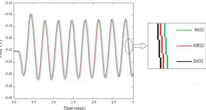
Considering the RF oscillator, Figure 10 shows its transient simulated output waveform obtained by ISE TCAD simulation. In a real circuit, the oscillation starts due to noise or an interferer coupling into the oscillator. In simulations to start the oscillation, it was necessary to provide a current impulse. The operating point and amplificatory gain have been chosen in order to obtain a very stable output signal. Since the LC tank network is composed only of reactive components, the oscillating signal maintains its amplitude without at-tenuation.
We present in figure 11 an oscillation typical case: T 335.8 Ps or f 2.97 GHz; the simulation was achieved for different gate insulators such as: SiO2, HfO2 and ZrO2. The nature of the oxide little affects the period of the signal against the signal quality.
Fig. 10a– Typical response of the DGMOSFET oscillator for different dielectric oxide
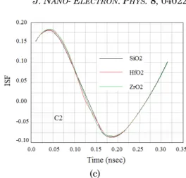
We can observe in figures 10a, 10b, and 10c, that the ISF function is sinusoidal with a period of 3 GHz which is the nearly same period of the output signal for differ-ent dielectric oxide.
The sine wave form observed for the oxide gate SiO2 as predicted by the theory [10, 11] is maintained for the ZrO2 and HfO2 dielectrics. We note clearly that the ISF function depends on the injection node and of the type of the gate dielectric.
The period of about 3 GHz is noted which is nearly the same period as the output signal.
5. CONCLUSION
The paper presents an analysis of a Double Gate MOSFET transistor and its use in a Colpitts oscillator.
(a)
(b)
(c)
Fig. 11– ISF function for current pulses for different dielec-tric oxide in: (a) inductance L, (b) capacitance C1, (c) capaci-tance C2
First of all, we have focused on the DC characteris-tics of the considered device. A 2D quantum model has been considered. The results show that there is no nota-ble difference between the SiO2, HfO2 and ZrO2 dielec-trics not only for current drain evolution but also for the phase noise scheme. The essential benefit of the high-k permittivity (case of HfO2 and ZrO2 material) is related to a notable reduction of the gate leakage current. In addition, we have pointed of, in this paper, that the noise performances of the oscillator are not affected by the high-k technology. Indeed, we have gone further on phase noise theory such oscillator, starting with mixed mode analysis of a LC type oscillator, through a new lecture of the ISF function. Our numerical simulation raw results are very agreed with theoretical precisions.
So, the finding of the paper is the high-k dielectric materials have an impact on the gate leakage current of the device and there is no notable difference in the drain current. It also states that the phase noise of a Colpitts oscillator is not affected by the use of the high-k materi-als.
REFERENCES
1. Z. Ren, R. Venugopal, S. Datta, M.S. Lundstrom, D. Jovanovic and J.G. Fossum IEDM Tech. Digest, 715 (2000).
2. T. Tosaka, K. Suzuki, H. Horie, T. Sugii, IEEE Electron. Dev. Lett.15 No 11, 466 (1994).
3. H. Lu, Y. Taur, IEEE T. Electron. Dev. 53 No 5, 1161 (2006).
4. B. Ray, S. Mahapatra, IEEE T. Elecron. Dev.56 No 2, 260 (2009).
5. S.L. Tripathi, R. Mishra, R.A. Mishra, J. Electron. Dev.16, 1388 (2012).
6. S. Chang, H. Shin, J. Korean Phys. Soc. 41, 932 (2002). 7. TC. Lim, G.A Armstrong, Solid-State Electron. 51, 320
(2007).
8. B. Razavi, IEEE J. Solid-State Circuits 31 No 3, 331 (1996).
9. J. Craninckx, M.S.J. Steyaert, IEEE J. Solid-State Cir-cuits32 No 5, 27 (1997).
10. A. Hajimiri, T. Lee, IEEE J. Solid-State Circuits33 No 2, 179 (1998).
11. A. Hajimiri, T. Lee, IEEE J. Solid- State Circuits35 No 3,
326 (2000).
12.D.B. Leeson, Proc. IEEE54 No 2, 329 (1966).
13. A. Hajimiri, T. Lee, IEEE J. Solid-State Circuit 34 No 5, 716 (1999).
14. A. Hajimiri, S. Limotyrakis, T. Lee, IEEE J. Solid-State Circuit34 No 6, 790 (1999).
15. M. Bella, S. Latreche, S. Labiod, Proceedings of the 11th International Conference on Computational and Mathe-matical Methods in Science and Engineering (Benidorm: Spain: 2011).
16. D. Rechem, S Latreche, C. Gontrand, Pramana J. Phys. 1 (2009).
17. Z. Ren, Ph.D. International Conference on Simulation of Semiconductor Processes and Devices (IEEE Xplore Mon-terey: 2006).
18. L. Yang, C. Shuqing, R.W. Dutto, International Conference on Simulation of Semiconductor Processes and Devices
(IEEE Xplore: Monterey, CA: 2006).
19. ISE-TCAD Manuals, Release 8.0, Integrated Systems Engineering (2002).
Microelectronics, ICM, (2008).
21.A. Demir, A. Mehrota, J. Roychowdhury, IEEE Circuit System47 No 5, 655 (2000).
22.L.S. Cutler, C.L. Searle, P. IEEE54 No 2, 136 (1966). 23.M. Bouhouche, S. Latreche, C. Gontrand, J.
Semiconduc-tors34 No 2 (2013).
24.Atlas, SILVACO-TCAD, International, Santa Clara, Sep-tember (2004).
25.D.L. Schafetter, H.K. Gummel, IEEE T. Elecron. Dev. 16
No 1, 64 (1969).
26.M. Kwok, K. Ng, Physics of semiconductor devices (Wiley: 2007).
27.D. Munteanu, J.L. Autran, V. Ferlet-Cavrois, P. Paillet, J. Baggio, K. Castellani, IEEE T. Nucl. Sci, 54 No 4, 994 (2007).
![Fig. 1 a – Schematic cross sectional structures of DGMOS with High-k technology, b – SEM image (Scanning electron microscopy) of DGMOS [16]](https://thumb-eu.123doks.com/thumbv2/123dok_br/16471030.199069/2.892.104.428.222.558/schematic-sectional-structures-dgmos-technology-scanning-electron-microscopy.webp)
![Figure 3 illustrate a real space and k-space distribu- distribu-tion of electrons within a 1D sub-band in the ballistic transport limit [17]](https://thumb-eu.123doks.com/thumbv2/123dok_br/16471030.199069/3.892.126.397.255.434/figure-illustrate-distribu-distribu-electrons-ballistic-transport-limit.webp)