American Journal of Engineering Research (AJER)
2016
American Journal of Engineering Research (AJER)
e-ISSN: 2320-0847 p-ISSN : 2320-0936
Volume-5, Issue-5, pp-105-108
www.ajer.org
Research Paper Open Access
w w w . a j e r . o r g
Page 105
Varactor Modelling for Power Factor Correction in a Varying
Load
Agwu D. D., Dike D. O., Ogu R. E. and Afamefule M.S.
Dept. of Elect. Engr., Federal University of Technology, Owerri, Imo State, Nigeria.
ABSTRACT:
For efficient system operation, it is desirable to keep the power factor at, or very close to unity. One of the very often used methods is application of suitable power factor correction technology. Capacitors are good candidate for constant load power factor correction due to suitability and cost effectiveness. However for varying loads, synchronous condensers are preferred despite having high initial cost as a result of their being able to supply varying leading or lagging reactive power; according to their field excitation. Due to the high acquisition and operation cost of synchronous condensers, this paper presents varactors as a possible alternative for power factor correction. These are diodes that vary their capacitances and leading reactive power according to supply voltage. Applying this involves looking at variation of power factor with supply voltage; and the option of aggregating and harnessing the junction capacitance of varactors for power factor correction of varying loads at low voltage AC levels. This innovation may lead to great improvement in distribution systems requiring quality power supply.KEY WORDS:
Varactor, power factor, varying load, diodes, junction, capacitanceI.
INTRODUCTION
Power factor of any device is simply the ratio of real power to apparent power drawn by the device. It tells how efficient a device is using drawn current. We can get power factor with other parameters such as calculating the ratio of pure resistance to total impedance, the cosine of the angle between current and voltage vectors. Power factor correction are just techniques by which the ration of real power to reactive power is improved. Power
factor can only be valued between 0 and 1 (0 ≤ cosϕ≤ 1) and power factor correction entails making the power
factor to approach 1.
So far, the technologies used for power factor correction are: use of synchronous condensers (motors and generators) and use of capacitors (also known as static var method) [1, 2]. In this paper, we will be discussing use of varactors as a third possible method. Before then we will just highlight the first two technologies presently being used extensively as follows:
Use of synchronous condensers: This is actually the use of over excited synchronous motor to provide leading reactive power to a system in other to cancel out lagging reactive powers. Though this method can be easily controlled and automated to achieve close to unity power factor, it is very costly compared to use of static vars (second method) as described below [3]. Excitation of synchronous generators can be varied too to alter the magnitude of leading or lagging reactive power it generates alongside the real power in order to balance the power system.
Use of Static Vars: This involves use of capacitors of appropriate capacitance and voltage to provide leading reactive power to cancel out lagging reactive power through provision of capacitive reactance which cancels out inductive reactance [2, 4].
II.
CAPACITOR RATED VOLTAGE AND CIRCUIT CONNECTION
Capacitors for power factor correction are best connected per phase and not line to line [5]. This is because line to line connection will increase the voltage level the capacitor will see at its nodes, thereby requiring that the capacitor have a higher voltage handling capacity. Cost of capacitors varies directly with the voltage capacity due to the fact that materials to handle high voltages and particular operating conditions gets increasingly scarce as voltage increases. So in all our calculations we are going to assume single phase connections. Where three phase connection is required, the connection must be in star and not delta [6, 5, 7].
For a single phase AC load, power required to drive the load is given equation (1):
American Journal of Engineering Research (AJER)
2016
w w w . a j e r . o r g
Page 106
In the above expression, is real power, is current drawn, is supplied voltage while is the power factor. If the power factor is of interest and all other parameters are known, the power factor may then be calculated as follows:
(2)
CAPACITANCE RELATIONSHIPS
As mentioned earlier, power factor correction involves injection of suitable reactive power to counteract the other. In improving a lagging power factor, a leading reactive power is introduced [1, 2]. With reference to both power triangle model, complex power relationships is given as follows:
(3)
Where S is the apparent or complex power, P is the real power and Q is the reactive power. Q is comprises of lagging reactive power and leading reactive power .Given that reactive power relationship with voltage and reactance is given as:
(4)
Where capacitive reactance is given by:
(5) Putting equation (6) into (5), we obtain:
(6)
Equation (6) shows that for a constant frequency and voltage , a continuous increase in capacitance will result to a continuous increase in leading reactive power. As the leading and reactive powers continue to counteract power factor in improved from 0 to 1, provided the leading reactive power did not exceed the lagging reactive power. A varying is device that has varying impedance. As illustrated in equation (3) and (6) it is required that capacitance increases (to increase leading reactive power) as lagging reactive power increases in order to maintain a good power factor or have it improved.
III.
APPLYING VARACTORS IN POWER FACTOR CORRECTION
The word VARACTOR is derived from VARiable reACTOR. Reactors are circuit elements like inductor and capacitor that can generate or absorb reactive powers. Hence varactor diode refers to PN junctions designed to be used as variable capacitor (reactor) in electrical circuits. The PN junction capacitance differ from that of a standard capacitor in that the diode capacitance monotonically decreases with increasing reverse bias [8].
For a diode to be effectively used as a varactor, it has to be in reverse bias mode [8]. This is because the diode creates a short circuit if forward biased since its forward bias resistance is always very negligible. In this mode, the reverse bias breakdown voltage and reverse bias conductance are of very big interest. While the reverse bias break down voltage determines the maximum voltage the diode can handle, the reverse bias conductance determines the leakage current of the varactor. It is desired that be as big as possible while be as small as possible.
IV.
VARACTOCR CARRIER CONCENTRATIONS
The carrier concentrations of the PN junction materials determines the magnitude of the following reverse bias voltage, forward and reverse bias current characteristics as well as built in potential [9, 8]. Though these factors mentioned must be considered pegged at a good value for the diode to be used as a varactor, the do not affect the junction capacitance after device fabrication. Hence, carrier concentration is only of interest during device modelling and fabrication. On the other hand, the voltage applied to the varactor becomes a determining factor for the junction capacitance.
For a non-degenerate doping, the relationship between reverse bias voltage and carrier concentrations is as follows:
(7)
Equation (7) indicates that one has to reduce carrier concentration to get a higher value of reverse bias voltage. In the market today, the 1n400x diode series can withstand a reverse bias voltage up to 1KV [10]. This is far more than the distribution voltages (415V) used in Nigeria.
American Journal of Engineering Research (AJER)
2016
w w w . a j e r . o r g
Page 107
V.
CAPACITANCE OF REVERSE BIASED PN JUNCTION
From energy band model of PN junctions and carriers action models, the diode capacitance is analogously modelled to be [8]:
(8) is the area of PN junction, is the semiconductor dielectric constant, is the permittivity of free space and is the width of the junction depletion region.
After device fabrication remain constant and varies to determine the junction capacitance of the varactor [11, 8]. Hence, the junction capacitance ( ) is inversely proportional to the junction depletion region ( ). Depending on whether the junction is asymmetrical step junction or linearly graded junction, is given by the equations (9) & (10):
- - - asymmetrical step junction (9)
- - - linearly graded junction (10) Where is the doping concentration of the lightly doped side of the asymmetrical step Junction and
is the linear grading constant. is the reverse voltage applied while is the built in potential.
…. (11)
Where respectively corresponds to the asymmetrical step junction and the one sided linearly step junction. If the doping concentration moves away from the junction and is said to be hyper-abrupt [12]. Hyper-abrupt junction can be formed by ion implantation or epitaxy. Built in potential on the other hand is given by:
(12) Where , and are Acceptor, Donor and Intrinsic concentrations. K is Boltzmann constant, T is temperature in Kelvin while is electron charge.
It is more convenient to work with a generalized relationship valid for a wide range of profiles. Hence instead of just substituting equations (9) or (10) separately into (6), we substitute a modified junction with as expressed below:
(13)
For , equation (13) reduces it to (9). Also, setting equation (13) reduces it to (10). Substituting equation (13) into (8) we obtain:
(14)
To investigate how varies with , it is often convenient to express junction capacitance as follows:
(15)
Where is the junction capacitance when the diode is unbiased and is given by:
(16)
VI.
RECOMMENDED VARACTOR CIRCUIT TOPOLOGY
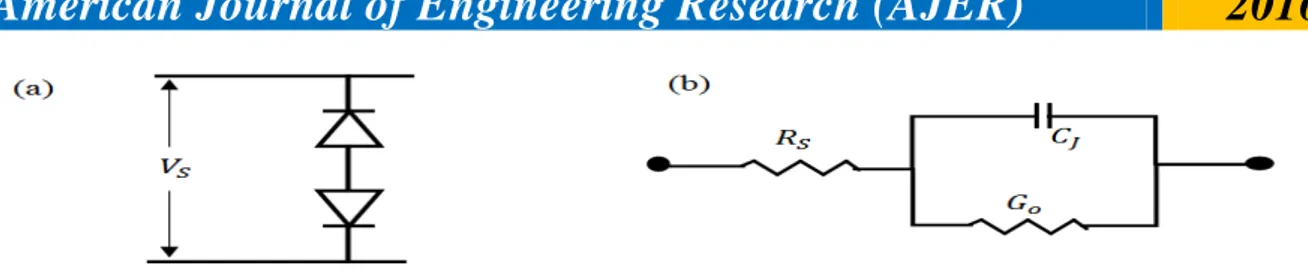
AC signals are characterized by the periodic reversal of their polarities. For a diode, this implies that while handling a AC signal, a reversed bias diode will become a forward biased diode and vice versa at every 0.02 seconds. Of course, when it becomes forward biased it creates a short circuit fault [12]. To overcome this challenge, we recommend that two diodes be placed back to back to form a single varactor.
American Journal of Engineering Research (AJER)
2016
w w w . a j e r . o r g
Page 108
VII.
ACCUMULATING HUGE CAPACITANCE
PN junction capacitance is always small compared to the magnitude of capacitance required for a real life power factor correction. To get a higher capacitance, PN junctions may be arranged in parallel as shown in figure 2 below. An analysis of number of 1n4007 diodes required to correct power factor of a 5W compact fluorescent lamp operating at 230V, 0.038A and 50Hz indicates that it will require over 23585 diodes will be required. Hence, accumulating required capacitance by just arranging diodes as illustrated maybe cumbersome. The best way out is to use integrated circuits manufactured by paralleling PN junctions of the same made up of similar carrier concentration to 1N400x series.
VIII.
CONCLSION
Equation (14) shows that a varactor’s capacitance increases exponentially as voltage. From equation (2) power factor decreases as voltage increases implying that lagging reactive power increases too. Since increase in applied voltage across a varactor increases its capacitance; as expresses in equation (14), which in turn increases leading reactive power which counteracts lagging reactive power to maintain power factor close to unity; as illustrated in equation (3) and (6). We are convinced that varactor set up as presented in this paper can be successfully maintain a pegged power factor in a varying load. This method offers great advantage because it will at any point vary its capacitance to maintain a designed power factor value unlike static vars that may supply too much capacitance. Of course too much capacitance causes low leading power factor, which is as bad as low lagging power factor.
References
[1] Mukesh K and G.k panda,” Comparative Study Of Power Factor Correction And THD Minimization Using Boost Converter And
Interleaved Boost Converter Using PI Controller,” IIAREEIE, vol.4, issue 1, pp150-158, Year 2015.
[2] F. C. Lee, M. M. Jovanovic, and D. Borojevic, “Analysis and design of power factor correction circuits,” in Proc. Virginia Power Electron. Ctr.(VPEC) Sem., 1996.
[3] Aparna Sarkar, “Automatic Power Factor Correction by Continuous Monitoring”, IJEIT, vol. 4, Issue 10, April 2015.
[4] Anagha S and Pranjali S, “Power Factor Correction Using PIC Microcontroller”, IJEIT, vol. 3, Issue 4, October 2013.
[5] Oscar García et al, “Single Phase Power Factor Correction: A Survey.” IEEE Trans. Power Electronics, vol. 18, no. 3, May 2003.
[6] Jaehong Hahn et al, “A New Three-Phase Power-Factor Correction (PFC) Scheme Using Two Single-Phase PFC Modules” IEEE
Trans. Industry Applications. vol. 38, no 1. Jan/Feb 2002.
[7] Murad Ali, “Design and Implementation of Microcontroller-Based Controlling of Power Factor Using Capacitor Banks with
Load Monitoring” Global Journal of Researches in Engineering Electrical and Electronics Engineering Vol. 13, Issue 2, Version
1.0, Year 2013.
[8] Robert F. Pierret, Semiconductor Device Fundamentals. California: Addison-Wesley, 1996. [9] S.O. Kasap, Optoelectronics and Photonics: Principles and Practices. Amsterdam: Pearson, 2013
[10] FairChild General Purpose Rectifiers [Online] Available: https://www.fairchildsemi.com/datasheets/1N/1N4007.pdf [11] Donald A. Neamen,Semiconductor Physics and Devices Basic Principles, 3rd ed. Boston: McGraw Hill, 2003.