UNIVERSIDADE NOVA DE LISBOA
Faculdade de Ciências e Tecnologia
Departamento de Engenharia Electrotécnica e de Computadores
Digitally Programmable Delay-Locked-Loop
with Adaptive Charge Pump Current for
UWB Radar System
por
Bruno Miguel Lopes
Dissertação apresentada na Faculdade de Ciências e Tecnologia da
Universidade Nova de Lisboa para obtenção do grau de
Mestre em Engenharia Electrotécnica e Computadores.
Orientador: Nuno Filipe V. Paulino
Acknowledgements
It was a long road until the end of this thesis, nevertheless I would never have had finished it without the support, patience and love from my family. A special kiss and hug to my dear sister because she will always be a part of my life.
When I ear the word teacher, the first name that occurs to me is of my advisor, Professor Nuno Paulino whose support and knowledge made this thesis possible. It was a great pleasure having him as my advisor.
For last, but with a great importance in my life, to Cintia the love of my life. Thanks for everything.
UNIVERSIDADE NOVA DE LISBOA
Abstract
Faculdade de Ciências e Tecnologia
Departamento de Engenharia Electrotécnica e de Computadores
Mestre em Engenharia Electrotécnica e de Computadores
by Bruno Miguel Lopes
The objective of this thesis is to study and design a digitally programmable delay locked loop for a UWB radar sensor in 0.13 µm CMOS technology.. Almost all logic systems have a main clock signal in order to provide a common timing reference for all of the components in the system. In certain cases it is necessary to have rising (or falling) edges at precise time instants, different from the ones in the main clock. To create those new timing edges at the appropriate time it is necessary to use delay circuits or delay lines. In the case of the radar system its necessary to generate a clock signal with a variable delay. This delay is relative to the transmit clock signal and is used to determine the target distance. Traditionally, delay lines are realized using a cascade of delay elements and are typically inserted into a delay-locked-loop (DLL) to guaranty that the delay is not affected by process and temperature variations. A DLL works in a similar way to a Phase Locked Loop (PLL).
Contents
Acknowledgements 1
Abstract 3
List of Figures 6
List of Tables 8
Abbreviations 9
1 Introduction 11
1.1 Background and Motivation . . . 11
1.2 Thesis Organization . . . 11
1.3 Contributions . . . 12
2 UWB Systems 14 2.1 Introduction . . . 14
2.2 UWB RADAR Systems . . . 16
3 Delay-Lock Loop (DLL) 19 3.1 Introduction . . . 19
3.2 Digitally Programmable DLL . . . 20
3.3 DLL Constituting Blocks . . . 26
3.3.1 Phase Detector . . . 26
3.3.2 Charge Pump . . . 27
3.3.3 Loop Filter . . . 29
3.3.4 Voltage Control Delay Line . . . 30
4 Design and Simulation Results 31 4.1 Differential Buffer . . . 31
4.2 Replica Bias . . . 33
4.3 Differential Buffer with Variable Delay . . . 37
Contents 5
4.4 Replica Bias for the Variable Delay Buffer . . . 40
4.5 Voltage Controlled Delay Line . . . 43
4.6 Phase Detector . . . 45
4.7 Charge Pump . . . 46
4.8 Biasing Circuit for the Charge Pump . . . 52
4.9 Differential to Single Ended Signal Converter. . . 54
4.10 Digitally Programmable DLL . . . 55
List of Figures
2.1 UWB Fractional bandwidth compared with narrow band systems [1]. . . . 15
2.2 Simple diagram of the RADAR operation principle. . . 16
3.1 Architecture of the Delay Lock Loop. . . 20
3.2 Architecture of the digitally programmable DLL. . . 21
3.3 System resolution (in bits) of the DLL for different closed loop frequencies and a Σ∆ modulator order of 1, 2 and 3. . . 22
3.4 System resolution (in bits) of the DLL for different closed loop quality factor and a Σ∆ modulator order of 1, 2 and 3. . . 22
3.5 DLL closed-loop frequency response. . . 24
3.6 Step response of the DLL. . . 25
3.7 Simulated output delay error, rms jitter value and peak-to-peak jitter. . . . 25
3.8 Schematic of the phase detector. . . 26
3.9 Schematic of single ended charge pump.. . . 27
3.10 Differential charge pump architecture.. . . 28
3.11 Common mode feedback circuit scheme. . . 29
3.12 Architecture of the voltage controlled delay line (VCDL). . . 30
4.1 Differential buffer schematic. . . 31
4.2 Plot of the buffer output voltage for a load resistor value equal to 4 KΩ. . 32
4.3 Replica bias principle. . . 33
4.4 Replica bias circuit schematic. . . 34
4.5 Schematic of the differential buffer with symmetric loads. . . 37
4.6 Architecture of the replica bias for the variable delay buffer. . . 40
4.7 Replica bias for the variable delay buffer circuit schematic. . . 40
4.8 Simulated delay of the VCDL as a function of the control voltage. . . 43
4.9 Simulated gain curve of the VCDL. . . 44
4.10 Flip-flop circuit schematic. . . 45
4.11 Differential AND gate circuit schematic. . . 45
4.12 Folded cascode charge pump circuit schematic. . . 46
4.13 Common mode comparator circuit. . . 48
4.14 Biasing for the charge pump circuit schematic. . . 52
4.15 Design of transistor MN2_B . . . 53
4.16 Differential to single ended conversion circuit and second pole. . . 54
4.17 Architecture of the digitally programmable DLL. . . 55
List of Figures 7
4.18 CMOS switches circuit schematic. . . 56
4.19 Simulated step response of the DLL. Programmable delay from 20 ns to 99 ns. . . 57
4.20 Simulated output delay as a function of the programming delay. . . 57
4.21 Jitter noise simulation results of the programmable DLL. . . 58
4.22 Architecture of variable charge pump current. . . 59
4.23 Simulated step response of the DLL. Programmable delay from 20 ns to 99 ns. . . 60
4.24 Simulated output delay as a function of the programming delay. . . 61
4.25 Delay relative error simulation results of the programmable DLL. . . 61
List of Tables
3.1 Charge Pump operation table. . . 28
4.1 Buffer design summary for a bias current equal to 100 µA. . . 33
4.2 Replica bias simulation results. . . 36
4.3 Corners analysis simulation results confirming the stability of the loop. . . 36
4.4 Replica bias design summary. . . 36
4.5 Buffer design summary for a bias current equal to 100 µA. . . 39
4.6 Replica bias for the variable delay buffer simulation results. . . 41
4.7 Corners analysis simulation results confirming the stability of the loop. . . 42
4.8 Replica bias for the variable delay design summary. . . 42
4.9 Truth table of the differential AND gate. . . 46
4.10 Charge pump simulation results.. . . 50
4.11 Corners analysis simulation results confirming the stability of the loop. . . 51
4.12 Charge pump design summary. . . 51
4.13 Common mode comparator design summary. . . 51
4.14 Biasing circuit design summary. . . 53
4.15 Differential to single ended design summary. . . 55
4.16 CMOS switches design summary. . . 56
4.17 Closed loop frequency pole (fp) and quality factor (Qp) simulations results with variable charge pump current. . . 59
4.18 Programmable delay results summary. . . 62
Abbreviations
CMOS Complementary Metal-Oxide-Semiconductor
CP Charge Pump
DLL Delay LockedLoop
FCC Federal CommunicationsCommission
GBW Gain BandWidth Product
NMOS Nchannel Metal-Oxide-Semiconductor
PD Phase Detector
PLL Phase LockedLoop
PMOS Pchannel Metal-Oxide-Semiconductor
PRF Pulse RepetitionFrequency
RADAR RAdio Detection And Ranging
rms root mean square
Σ∆ Sigma Delta modulator
UWB Ultra Wide Band
VCDL Voltage Controlled Delay Line
VCO Voltage Controlled Oscillator
Dedicated to my Family. . .
Chapter 1
Introduction
1.1
Background and Motivation
The objective of this thesis is the study and design of a digitally programmable delay locked loop (DLL) for Ultra Wideband (UWB) Radar systems. A DLL is a feedback system, in many ways similar to a phase locked loop (PLL), where it produces a clock signal with a controlled delay.
In 2008, a book [2] was published with a study and design of a low-cost, low power radar sensor, using 0.18 µm CMOS technology. Traditionally radar systems are based on RF signals, the design in this book presented some new ideas and concepts since it was study for UWB signals. A new architecture for a digitally programmable DLL was presented. Based on this architecture, it is the objective of this thesis to present a more detail study and design of this digitally programmable DLL, using 0.13 µm CMOS technology.
There are some conference papers and articles presenting some ideas to design a DLL to achieve many purposes. In this thesis a design of a new technique based on making the charge pump current variable is presented.
1.2
Thesis Organization
The thesis is divided into 5 chapters, including this one. A brief overview of the following chapters is given next.
Chapter 1. Introduction 12 In chapter 2 a introduction of UWB radar systems is made, starting by explaining the definition of a UWB signal and some differences between a narrow band signal are pre-sented. Follow by some applications of UWB. The second part of this chapter explains the operation of a pulse radar system. Traditionally radar systems uses narrow band signals (sine wave carrier) and using short duration pulses requires a high carrier frequency. Since UWB signals don’t have a carrier wave it is possible to have a very short duration pulse resulting in a better radar resolution that can distinguish two targets in a given direction.
Chapter 3 presents an Delay Lock Loop (DLL) overview. The theory of operation of the DLL is explained, with some differences between a DLL and a Phase Lock Loop (PLL) presented. The purpose of the DLL in a radar system is explained as the need for having a digitally programmable DLL also. The architecture of this circuit can have a large programming linearity is presented and analyzed at high level, to meet the required specifications for the radar system. The digitally programmable DLL will generate a clock signal with a programmable delay. This delay is relative to the transmit clock signal and is used to determine the target distance. The electronic sub-blocks necessary to build this circuit are describe in detail as the proposed architectures. These circuits are implemented using differential clock signals in order to reduce the noise level in the radar system.
The fourth chapter describes the design and simulation results for all of the circuits needed to build the digitally programmable DLL. Simulation results of this circuit shows a high output jitter for large delays. A new architecture is proposed to deal with this problem, making the charge pump current variable. This solution will show improvements in the operation of the circuit.
The thesis ends with a final chapter dedicated to some final conclusions and further research suggestions.
1.3
Contributions
Chapter 2
UWB Systems
2.1
Introduction
Alternately referred to as impulse, baseband or zero-carrier technology, Ultra Wideband (UWB) systems transmit signals across a much wider frequency than conventional systems [3]. There are several signals that can be classified as UWB signals, these are typically constituted by a repetitive sequence of short pulses with a certain repetition frequency (PRF). The amount of spectrum occupied by a UWB signal, i.e. the bandwidth of the UWB signal (fractional bandwidthBf rac) is at least 25% of the center frequency. A narrow
band signal fractional bandwidth is inferior to 10%. For example, a UWB signal centered at 2 GHz would have a minimum bandwidth of 500 MHz and the minimum bandwidth of a UWB signal centered at 4 GHz would be 1 GHz. The formula proposed by the Federal Communications Commission (FCC) [4], that defines theBf rac is:
Bf rac=
2·(fH −fL)
fH −fL
(2.1)
wherefH is the upper frequency of the -10 dB emission point andfLis the lower frequency
of the -10 dB emission point. The center frequency of the transmission was defined as the average of the upper and lower -10 dB points and in given by the next expression.
fc =
fH +fL
2 (2.2)
Chapter 2. UWB Systems 15 Fig. 2.1 shows a comparison between the UWB fractional bandwidth and the narrow band systems.
Figure 2.1: UWB Fractional bandwidth compared with narrow band systems [1].
The most common technique for generating a UWB signal is to transmit pulses with du-rations less than 1 nanosecond. Because of the narrow or short duration of the pulses, that results in a large transmission bandwidth, UWB devices can operate using spectrum occupied by existing narrow band radio services without causing interference, thereby permitting scare spectrum resources to be used more efficiently [2]. Nevertheless any electronic or electric equipment always emits unwanted radiation that can interfere with narrow band radio systems, a example of this is digital systems such as computers. There-fore every electronic and electrical device is required to limit the power of these unwanted emissions level. The transmitted power of UWB devices is controlled by the Federal Com-munications Commission (FCC), so that narrow band systems are affected from UWB signals only at a negligible level [4].
UWB has several applications all the way from wireless communications to RADAR1
imaging, and vehicular radar. The ultra wide bandwidth and hence the wide variety of material penetration capabilities allows UWB to be used for radar imaging systems, including ground penetration radars, wall radar imaging, through-wall radar imaging, surveillance systems, and medical imaging. Images within or behind obstructed objects can be obtained with a high resolution using UWB. Similarly, the excellent time resolution and accurate ranging capability of UWB can be used for vehicular radar systems for collision avoidance, guided parking, etc. Positioning location and relative positioning
Chapter 2. UWB Systems 16 capabilities of UWB systems are other great applications that have recently received significant attention [5].
2.2
UWB RADAR Systems
The operation of a a pulsed radar system is very simple [6], an electromagnetic signal (pulse) is radiated, this signal travels at the speed of light (c) (assuming that the signal propagates in space), when the signal encounters an object (target) part of its energy is reflected back (re-radiated), therefore creating an echo, the echo signal travels back at the speed of light to the point of the radiation of the original signal. The radar can use a single antenna for transmission and reception of the pulse or two separate antennas. The radar operation principle is showed in Fig. 2.2.
Transmitter
Receiver
R
Target
T
Figure 2.2: Simple diagram of the RADAR operation principle.
The time interval (T) between the transmission of the signal and arrival of the echo can be measured, making the distance (or range) (R) at which the target is located possible to calculate using the following formula
R = c·T
2 (2.3)
The radar systems that this thesis is based on, is a low-cost, low power radar sensor. This radar sensor can have several applications such as a proximity sensor (detects any intruders that enter a predefined perimeter), a motion detector (detects motion of objects), a ground penetrating radar (detects objects buried at a small depth in some types of soil) and 2D/3D imaging (with more than one or two sensors and using signal processing techniques it is possible to obtain a 2D/3D image).
Chapter 2. UWB Systems 17 sensor is used to locate two different objects, then receiving two echoes at the same time will not be adequate. The time interval between two transmitted signal must be large enough so that the first echo will not be confused with the echo received from the second transmission. The time interval between two pulses must increase as the potential targets are located further away. The maximum Pulse Repetition Frequency (PRF) of a radar system is dependent on the maximum distance that a target can be detected. If, for example, the maximum range a target might be detected is 300 Km, the maximum value for the PRF would be limited to 500 Hz, but if the maximum range is 30 m, the maximum PRF value can be as high as 5 MHz [2]. The maximum range of the radar (Rmax) is given
by
Rmax =
c·TP RF
2 (2.4)
The PRF value is usually also selected so that echoes from outside the maximum radar range have an amplitude smaller than the minimum detectable amplitude by the radar receiver.
The echoes received by the radar receiver can have different shapes and longer duration than the transmitted pulse depending on the target shape and size. Considering this, it is possible that two echoes can be interpreted as one (the two echoes combined) in the radar receiver. Any two targets separated by a radial distance from the radar inferior to c.τ (whereτ is the pulse width) produce a combined echo signal that can be interpreted as the one created by a single target [2]. This means that the value of the pulse width will determine the resolution that the radar can distinguish two targets in a given direction. Traditional radar systems uses narrow band signal (sine wave carrier) and using short duration pulses requires a high carrier frequency. If a pulse signal is used to modulate a sine wave carrier, the resulting signal will have approximately the same bandwidth as the pulse signal centered around the carrier frequency. This is one of the advantages of the UWB signals, since they don’t have a carrier wave it is possible to have small pulse duration.
Chapter 2. UWB Systems 18 conditions might not be possible [2].
Chapter 3
Delay-Lock Loop (DLL)
3.1
Introduction
Almost all logic systems have a main clock signal in order to provide a common timing reference for all of the components in the system. In certain cases it is necessary to have rising (or falling) edges at a precise time instants, different from the ones in the main clock. To create those new timing edges at the appropriate times it is necessary to use delay circuits or delay lines [8].
In the case of the architecture of the radar system its necessary to generate a clock signal with a variable delay. This delay is relative to the transmit clock signal and is used to determine the target distance. Traditionally, delay lines are realized using a cascade of delay elements and are typically inserted into a delay-locked-loop (DLL) to guaranty that the delay is not affected by process and temperature variations [2].
A Delay Lock Loop (DLL) is a feedback system, where the delay produced by a voltage controlled delay line (VCDL) into a clock signal, is adjusted until is equal to one or more periods of the reference clock [8], [9], [2].
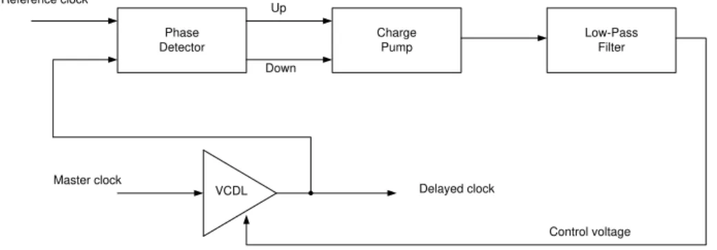
The DLL, as shown in Fig. 3.1, works in a similar way to a Phase Locked Loop (PLL). Instead of having a voltage controlled oscillator (VCO), the DLL has a voltage controlled delay line (VCDL) that does not suffer from jitter accumulation, since normally is not used in a closed loop configuration as the VCO.
The DLL loop compares the phase (delay) of the reference clock with the phase of the delayed clock using a phase detector (PD). The output of the charge pump (CP), goes through a low-pass filter to attenuate the excess jitter noise from the clock signals, and
Chapter 3. Delay-Lock Loop (DLL) 20
Phase Detector
Charge Pump
Low-Pass Filter
VCDL Master clock
Reference clock
Up
Down
Delayed clock
Control voltage
Figure 3.1: Architecture of the Delay Lock Loop.
the resulting voltage is used to control the delay value in the voltage controlled delay line (VCDL) until the rising (or the falling) edges of both clocks coincide. Since the output of the DLL is just a delay version of the master clock, the output frequency value is always the same as the input frequency.
3.2
Digitally Programmable DLL
In order to facilitate the operation of the radar system, it is important that the delay value should be digitally programmable. The maximum delay of the digitally programmable delay must be equal to 100 ns, corresponding to a radar range of 15 m, and a delay programming step smaller than 0.2 ns, corresponding to a ranging resolution smaller than 3 cm. If a large maximum delay and a small delay step is required, the delay line will be composed by a large number of delay elements [10], [11], each one having a delay equal to the delay step, in this case this approach would result in at least 256 delay elements (8-bit resolution) [2]. This would result in a large power dissipation and in a large area. Also this type of delay line suffers from element mismatch, resulting in limited delay resolution [12]. The digitally programmable delay will make each programming code correspond to a precise distance, if the delay resolution is limited then a programming code will not correspond to a precise distance. For these reasons the architecture for the digitally programmable DLL [13], will be as the one depicted in Fig. 3.2whose resolution is not affected by element mismatch and is only limited by the response time to a new programming code.
Chapter 3. Delay-Lock Loop (DLL) 21
ΣΔ
DLL Master clock
Delay
TD
Reference clock
Output clock
Figure 3.2: Architecture of the digitally programmable DLL.
In order to achieve a digitally programmable delay with a large linearity (independent from matching errors), the architecture of the system is constituted by a digitalΣ∆modulator that controls a 1-bit digital to time converter, whose output will be filtered by the DLL, thus producing the delayed clock signal [2]. The digital code apply to the digital Σ∆ will control the two switches that generate the reference clock. This clock is created with the help of the master clock and a delayed version of this same clock and will have an average delay value corresponding to the digital code. The delayed clock was a fixed delay equal toTD. To avoid spikes in the reference clock, the maximum delayTD should be inferior to
half period of the master clock. The reference clock will have a large jitter noise generated by the switching sequence that will be mostly filtered by the low-pass characteristic of the DLL.
The minimum order of the DLL is related to the order of theΣ∆, however the DLL must be a second-order system because of closed loop stability problems. The order of the Σ∆
Chapter 3. Delay-Lock Loop (DLL) 22
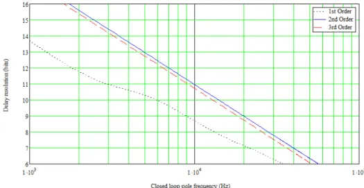
Figure 3.3: System resolution (in bits) of the DLL for different closed loop frequencies
and aΣ∆ modulator order of 1, 2 and 3.
This graph was calculated considering thatTD = 100 ns,Fclk = 2.5 MHz and that the loop
transfer function is a second order low-pass filter with a complex pole frequency given by
HDLL(s) =
W2
p
s2
+Wp
Qp ·s+W
2
p
(3.1)
The value of the closed loop pole frequency can be obtain considering that the program-ming resolution must be equal to 9 bits, resulting in fp ≈ 19.8 KHz corresponding to an
rms jitter of 56.03 ps. The closed loop pole quality factor Qp does not affect this graph
as long its value is between 0.5 and 1.5 as the Fig. 3.4 shows.
Figure 3.4: System resolution (in bits) of the DLL for different closed loop quality
Chapter 3. Delay-Lock Loop (DLL) 23 The DLL closed loop transfer function is obtained by a discrete time analysis resulting in [2]:
HDLL(z) =
G·IP ·KP D·KV CDL·TCLK ·z
G·IP ·KP D·KV CDL·TCLK +C1 ·τRC·(z−1)·(z−1 + TτCLK
RC )
(3.2)
whereG is a gain in the filter,IP is the charge pump current, KP D is the phase detector
gain, KV CDL is the gain of the VCDL, C1 is the output capacitance of the charge pump,
τRC is the time constant of a first order filter introduced in the loop in order to obtain a
second order transfer function. Evaluating this equation usingz =ej·2·π·f ≈1 +j·2·π·f
it is possible to obtain an approximated continuous time transfer function. From this transfer function it is possible to obtain expressions for the closed loop pole frequency and quality factor:
fp =
1 2π
r
KP D·KV CDL·
IP
C1 ·
1
τRC ·
Fclk (3.3)
Qp =
q
KP D·KV CDL· ICP
1 ·
1
τRC ·Fclk
1
τRC +KP D·KV CDL·
IP
C1 ·
1
τRC
(3.4)
These expressions are used to design the DLL loop in order to have the desired fp and
Qp values. The main circuit parameters used in this design are ICP
Chapter 3. Delay-Lock Loop (DLL) 24
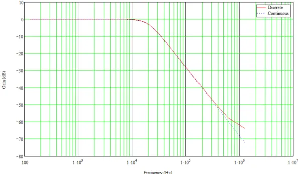
Figure 3.5: DLL closed-loop frequency response.
According to the graph, the attenuation of the DLL discrete transfer function is smaller than the the continuous one at high frequencies, causing an increase in the output jitter noise since the input jitter noise is located mainly at high frequencies [2]. Therefore the programing resolution will be smaller than the values shown in Fig. 3.3 and consequently the value of the closed loop pole frequency (fp) will be smaller than the predicted 19.8
KHz. In fact, after simulation the discrete transfer function with the predicted fp, a
rms jitter value of 73.39 ps and a resolution of 8 bits is obtained. To achieve the 9 bits resolution, simulations results in afp value of 16 KΩand a Qp value of 0.7 corresponding
to a rms jitter value of 47.69 ps (smaller than the predicted value of 56.03 ps). This results correspond to IP
Chapter 3. Delay-Lock Loop (DLL) 25
Figure 3.6: Step response of the DLL.
The real delay, the rms and peak-to-peak value of the jitter noise are measured by simu-lating the DLL discrete model with different delays selected. The results are depicted in the next figure.
Figure 3.7: Simulated output delay error, rms jitter value and peak-to-peak jitter.
Chapter 3. Delay-Lock Loop (DLL) 26
3.3
DLL Constituting Blocks
3.3.1
Phase Detector
A phase detector (PD) is a circuit whose average output,Vout, is linearly proportional to
the phase difference,∆φ, between its two inputs [14]. The typical example of a PD is the exclusive OR (XOR) gate. As the phase difference between the inputs varies so does the width of the output pulses, thereby providing a dc level proportional to ∆φ. The XOR phase detector is not suitable to this design since it detects phase differences in both rising and edges of the input signals. Instead a PD architecture depicted in Fig. 3.8 is selected. This PD is a digital state machine with 3 states, whose state transitions are determined by the rising (or falling) edges of the input clock signals [15]. The schematic of the PD is shown next
UP
DOWN
“1”
“1”
CLK1 CLK2 RESET D clk Q D clk Q R R
Figure 3.8: Schematic of the phase detector.
The 3 states correspond to the clock signal (CLK1) being "ahead", being the same or
being "behind" of the clock signal (CLK2). Initially the PD is in inactive state, both UP
and DOWN signals are OFF, if the rising edges of CLK1 occur before the CLK2, then
the PD will activate the UP signal until a rising edge of CLK2 occurs, resulting in the
activation of the DOWN signal that will activate the RESET signals, returning to the inactive state. The time interval when the UP signals is ON measures the phase difference between the two input clock signals. The third state is the other way around, when the rising edge of CLK2occurs first and the DOWN signal is activated. The maximum amount
of delay between the two clock signals with the same period (Tclk) is ±Tclk. When the
Chapter 3. Delay-Lock Loop (DLL) 27 state at start-up, this is implemented with an OR gate and a new reset signal (generated at start-up), as shown in Fig. 3.8.
In this circuit, the minimum phase difference detected, is limited by the speed of the flip-flops and the AND gate. If the rising edge of the clock signals is very close, the RESET signal starts to activate before the outputs of the flip-flops have completely settled at the ON value, resulting that the outputs of the flip-flops resets before stabilizing. For very small phase differences this process causes the UP and DOWN signals not to activate at all and the phase difference is not detected. The solution to this problem is very simple [16] if a small delay is added to reset path, the UP and DOWN signals are always activated (even for zero phase difference) during a minimum time equal to the added delay. Now even a very small phase difference between the input signals is capable of generating a difference between the ON time of the UP and DOWN signals.
3.3.2
Charge Pump
To fully understand the operation of the charge pump (CP) it is better to first describe the operation of a single ended CP as show in Fig. 3.9 [17].
Vout
S1
S2
C UP
DOWN
Figure 3.9: Schematic of single ended charge pump.
Chapter 3. Delay-Lock Loop (DLL) 28 source will supply current to the output capacitor increasing the output voltage. When the DOWN control signal is active the switch S2 is turned ON and the NMOS current source will sink current from the capacitor decreasing the output voltage. Since the behavior of PMOS and NMOS transistors are different, due to matching errors, the supply current and the sink current will not be equal. This is one the biggest problems in a singled ended CP.
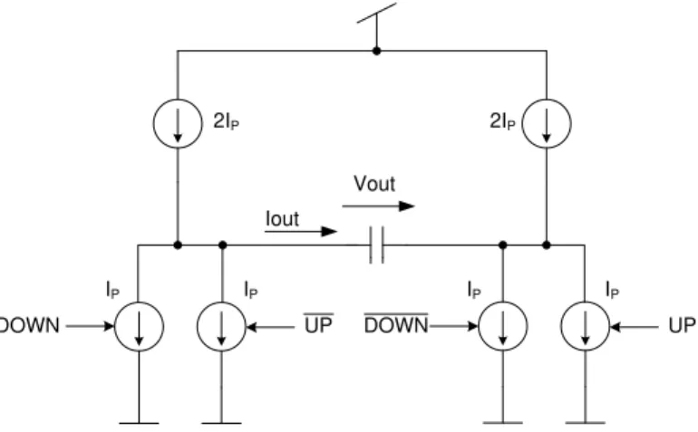
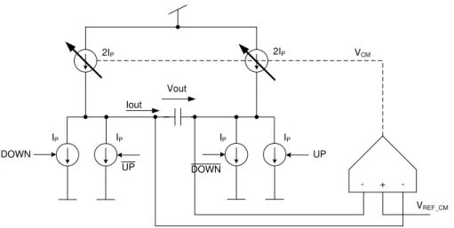
The CP architecture will be fully differential, as show in Fig. 3.10 since has several advantages over the conventional single-ended charge pump proposed in [18], [19], [20]. The output current will have symmetrical values for the up and down current and the output voltage is more immune to common mode noise [2]. The main disadvantage of the differential CP is the output resistance, since even when the charge pump is OFF, the current sources remain connected to the output node. This problem does not occur in the single ended architecture where the output resistance is almost infinite in the OFF state. This subject will be addressed later in the design chapter.
2IP 2IP
IP IP IP IP
UP UP
DOWN DOWN
Vout
Iout
Figure 3.10: Differential charge pump architecture.
Up Down Iout
0 0 0
0 1 -IP
1 0 +IP
1 1 0
Table 3.1: Charge Pump operation table.
This CP is design to have a high output resistance, this means that any mismatch between the current values of the NMOS and PMOS current sources would result in the common mode output voltage saturating in either VDD or GN D [2]. To avoid this situation it is
Chapter 3. Delay-Lock Loop (DLL) 29
2IP 2IP
IP IP IP IP
UP DOWN Vout Iout + -UP DOWN VREF_CM VCM
Figure 3.11: Common mode feedback circuit scheme.
The common mode voltage is adjusted comparing the output common voltage with the desired common mode reference voltage and then using this error voltage adjust the current of the PMOS current sources. This operation is equivalent to
Vo_CM =
Vop+Vom
2 −VREF_CM
·G=
Vop−VREF_CM
2 +
Vom−VREF_CM
2
·G
(3.5)
whereG is the common voltage gain of the CP.
3.3.3
Loop Filter
Chapter 3. Delay-Lock Loop (DLL) 30
3.3.4
Voltage Control Delay Line
The voltage controlled delay line (VCDL) must be able to produce a variable delay with a maximum value of 100 ns. Since only one delay element is unable to accomplish this task, a cascade of delay elements will be used. For a maximum delay value of 100 ns it will be necessary to use three variable delay elements followed by three fast buffers. The purpose of these last three buffers is to recover the rise and fall times of the clock signal after the delay is introduced. The delay of this delay line is three times the delay of a single variable delay buffer plus the delay of the fast buffer at the output. The architecture is depicted in Fig. 3.12.
Replica Bias Variable Delay
Replica Bias
VBias_N variable VBias_N
VBias_P
VIN VOUT
Chapter 4
Design and Simulation Results
4.1
Differential Buffer
This block is responsible for processing differential digital signals and it is composed by a differential pair and a resistive load, as shown in Fig. 4.1. The circuit, as the name
VIN+ V
IN-VBias_N
MN1
MD MD
RL RL
VOUT+ V
OUT-IB
Figure 4.1: Differential buffer schematic.
indicates, operates with differential digital signals, i.e., signals that have only two valid voltage levels, each representing a digital value. By applying a differential signal to the input, the differential pair will be in one of two operations regions, when bothMD
tran-sistors are ON (linear region), and when one of the trantran-sistors is ON and the other OFF (saturation region), producing two differential output voltage levels. A complete study of this two operations regions in shown in [2]. These voltage levels will have maximum
Chapter 4. Design and Simulation Results 32 value amplitude limited by the power supply (VDD), the Vdsat voltage of the transistor
MN1 and a safety margin voltage (Vtol)(approx. 120 mV) to guaranty that transistorMN1
is in the saturation region. The output voltage swing (Vswing) is determined by the buffer
bias current (IB) and by the load resistance value (RL) , using Ohm´s law
Vswing =RL×IB (4.1)
For the case of a bias current value of 100 µA and in order to obtain a voltage swing of 400 mV at the output, results inRL = 4 KΩ. A voltage swing of 400 mV requires that
VDD−Vdsat(MN1)−Vtol ≥Vswing (4.2)
where
Vdsat(MN1)≤680mV (4.3)
Transistor MN1 Vdsat voltage value is set to 400 mV and the channel lenght is set to 1.5
µm. The Vdsat voltage of the differential pair, MD, is set to 80 mV, a value small enough
to guaranty the saturation of the transistors by the input signal and the channel length is set to 120 nm. In Fig. 4.2, the simulation results of the design described above are shown.
Chapter 4. Design and Simulation Results 33 Vdsat (mV) L(µm) W(µm)
MD 80 0.12 7.5
MN1 400 1.5 3.7
Table 4.1: Buffer design summary for a bias current equal to 100 µA.
4.2
Replica Bias
In order to guaranty that the amplitude of the output voltage (Vswing) of the differential
buffer will be constant, it is necessary to use a replica bias circuit to compensate the variation of the value of the resistance output. This value can vary with process and temperature up to 30% of its nominal value. The replica bias principle will be to adjust the bias current (IB), by comparing the output voltage of a replica of the buffer circuit
to the desired value (Vref), using an amplifier. In fact only half of the buffer circuit is
needed since one of the outputs is VDD.
Therefore Vref = VDD - Vswing. The amplifier output voltage (VBias_N) determines the
value of the IB current through transistor MN1. This bias current of this half-buffer can
be mirrored to all the buffer circuits [21],[22]. The principle is shown in Fig. 4.3.
VIN+ V
IN-MN1
MD MD
RL RL
VOUT+ V OUT-IB VBias_N MN1 MD RL + -VREF VOUT
Figure 4.3: Replica bias principle.
The relative error between theVref voltage and theVout voltage depends on the feedback
loop gain of the replica bias and is given by
Vout
Vref
= 1
1 +A·gmM N1 ·RL
(4.4)
Chapter 4. Design and Simulation Results 34 single stage amplifier because using a low loop gain value (within the limits of the gain specification) improves the phase margin of the loop.
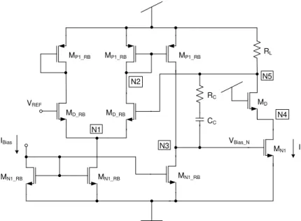
IBias
MN1_RB MN1_RB MN1_RB
MP1_RB
MP1_RB
MP1_RB
MD_RB MD_RB
VREF CC RC MD RL MN1 VBias_N N3 N1 N2 N5 IB N4
Figure 4.4: Replica bias circuit schematic.
The loop gain is given by
Gloop≈
gmD_RB ·gmN1·RL
gdsP1_RB+gdsN1_RB
(4.5)
As show in Fig. 4.4 the loop has a total of 5 poles, these are associated to the 5 nodes of the circuit in the signal path (N1 to N5). The dominant pole of the loop is located, by design, at node N3, its approximate expression can be obtained using Miller theorem and is given by
p3 ≈
gdsP1_RB +gdsN1_RB
CC ·(1 +gmN1·RL)
(4.6)
The gain bandwidth product (GBW) is given by (assuming a phase margin larger than 60◦)
GBW =p3·Gloop≈
gmD_RB
CC
(4.7)
The phase margin of the loop is determined by all the 5 poles of the circuit and by the 2 zeros, one zero created by the Cgs capacitance in the differential pair formed by the
MD_RB transistors and the other zero is associated to the compensation resistorRC. The
Chapter 4. Design and Simulation Results 35 and is calculated using
P M = 180◦−
X
arctan(GBW
−pi
)−Xarctan(GBW
−zi
)
(4.8)
The remaining poles are given by
p1 ≈ −
2·gmD_RB
2·CgsD_RB+Cp1
(4.9)
p2 ≈ −
gmP1_RB
2·CgsP1_RB +Cp2
(4.10)
p4 ≈ −
gmD
2·CgsD+Cp4
(4.11)
p5 ≈ −
gmN1·CC
Cp3·Cp5+CC ·Cp3+CC·Cp5
(4.12)
The value of Cp5 is small compared to the Cp3 value, it is approximately equal to Cp3 ≈
M·CgsN1, since the transistors inside the buffers controlled by the replica bias have the
same Vdsat voltages as the transistors of the half buffer. Under these condition the p5
expression can be further simplified to
p5 ≈
Vdsat_N1
M ·L2
N1
·K (4.13)
where K is technology dependent parameter.
As in any feedback loop, the replica bias amplifier must be designed to assure that the loop is unconditionally stable. Therefore the specifications for this circuit are a loop gain larger than 32 dB, since the control voltage VBias_N is essentially a DC signal, a GBW
larger than 100 kHz is enough, and phase margin larger than 60◦.
Inside the half-buffer the transistors have the same Vdsat voltages and channel lengths
as the transistors inside the differential buffer. To reduce the parasitic capacitance the channel length of transistors MD_RB should be small, therefore a value of 0.5 µm and
a Vdsat value of 100 mV are defined to obtain the largest possible gain and GBW values
for a given current value. The Vdsat values for the transistors MN1_RB and MP1_RB are
Chapter 4. Design and Simulation Results 36 is set to 2 µm to improve the gain and for the MP1_RB is set to 2 µm. The values of the
resistance and capacitor are selected together using AC simulations resulting in CC = 3
ρF andRC =4 kΩ. After the previous design process the circuit design goals were obtain
and are shown next in table4.2.
Design Typical Simulation Goals Results
Gain(dB) 32 44.2
GBW(MHz) 0.1 16.7
Phase(◦) 60 81.5
Table 4.2: Replica bias simulation results.
Since the simulations results can vary with temperature and supply voltage values, a corners analysis was made to assure that the loop is unconditionally stable.
Supply Voltage (V) Section Temperature (◦C) Gain (dB) GWB (MHz) PM (◦)
Vdd = 1.2
Slow 0 42.9 19.4 73.1
80 40.6 14.9 65.4
Fast 0 45.8 17.2 98.3
80 44.5 13.6 86.8
Vdd = 1.08
Slow 0 41.4 18.0 69.1
80 39.1 13.7 61.9
Fast 0 44.0 16.1 92.8
80 42.0 12.6 80.8
Vdd = 1.3
Slow 0 43.8 20.1 75.5
80 41.5 15.3 67.7
Fast 0 46.6 17.8 100.9
80 45.6 14.1 90.3
Table 4.3: Corners analysis simulation results confirming the stability of the loop.
This results showed that the circuit design parameters are well adjusted and the loop is unconditionally stable.
Vdsat(mV) L(µm) W(µm)
MD_RB 100 0.5 10
MN1_RB 300 2 8.8
MP1_RB 300 2 20
Chapter 4. Design and Simulation Results 37
4.3
Differential Buffer with Variable Delay
This circuit is used in the voltage controlled delay line (VCDL) to help produce a maximum value of 100 µs to accomplish the radar system specifications. The differential buffer in Fig. 4.1 can produce a variable delay [9], by changing the load resistance of the buffer using MOS transistors in the linear region. The differential buffer circuit with symmetric loads [9] is show in Fig. 4.5.
VIN+ V
IN-VBias_N
MN1
MD MD
MP1 MP2 VOUT+ V OUT-IB C VBias_P
MP1 MP2 VBias_P C
Figure 4.5: Schematic of the differential buffer with symmetric loads.
A PMOS transistor is in the linear region when VSD < VSG − |VT|, when this condition
applies the drain current is given by
ID =β·
(VSG− |VT|)·VSD−
V2
SD
2
(4.14)
where β = Kp · WL and Kp is the transistor transconductance which depends on the
technology and varies with process and temperature. The drain resistance of the transistor is calculated using
rsd =
dID
dVSD
−1
= 1
β·[(VSG− |VT|)−VSD]
(4.15)
The expression shows that the resulting resistor has a non-linear dependence on the VSD
voltage. TheVSG voltage should be as large as possible, compared to the maximum VSD
Chapter 4. Design and Simulation Results 38 linear region.
The drain current of the MP1 transistor is given by
ID =β·
(VSD
2 − |VT|)
·VSD (4.16)
The drain resistance ofMP2 transistor is given by expression 4.15and for MP1 transistor
is calculated using
rsd =
dID
dVSD
−1
= 1
β·(VSD− |VT|)
(4.17)
From expressions 4.15 and 4.17 it is possible to calculate the equivalent resistance from the symmetrical load resulting in
rsdeq. =
1
β·(VDD −VBias_P −2· |VT|)
(4.18)
The bias current of this circuit can be calculated using expression 4.14 and expression 4.16 resulting in
IB ≈
β
2 ·(VDD −VBias_P −VT)
2
+ β
2 ·(Vswing−VT)
2
(4.19)
This equation shows that the current in the buffer changes quadratically with both the control voltage (VBias_P) and the clock signal amplitude (Vswing).
If both PMOS transistors, in the symmetrical load, have the same size, this type of load exhibits an almost constant conductance, when the output voltage changes. The delay of each differential stage varies with the value of the load conductance, which can be adjusted using the control voltage VBias_P. The delay of the differential buffer is proportional to
the RC time constant of the output node and it can be calculated [2] using :
TD(VBias_P)≈
0.7×C
β·[(VDD−VBias_P −2· |VT|)]
(4.20)
From this expression it is clear that the delay depends only on the β, C and VBias_P
values and only this last one can be used to vary the delay. The minimum delay is obtained when the VBias_P is equal to 0 volt (VSG = VDD) and the maximum delay is
obtained whenVBias_P =VDD− |VT| −Vswing (VSG =Vswing +|VT|) corresponding to the
Chapter 4. Design and Simulation Results 39 The maximum delay a single buffer can add is limited to TDmax = TCLK/4 because a
larger delay would result in an output signal with an amplitude smaller than the input signal amplitude. Therefore if a larger delay value is required it is necessary to use more than one delay element in cascade. A voltage controlled delay line (VCDL) is designed in section3.3.4 to accomplish a larger delay.
The signal amplitude in this circuit must be large enough in order to guaranty that the differential pair saturates and that it is larger than the VT of the load transistors for all
the corners. The circuit is designed in order to have a voltage swing of 400 mV and a bias current (for the minimum delay case) of 100µA. The load PMOS transistors are designed to have a small channel length (L = 250 nm) and a smallW/Lratio. With this design the theoretical value to obtain the maximum delay is VBias_P = 470 mV. Simulation results
showed that this value could be approximate 670 mV. A larger value will not guaranty all of the design goals in the corner analysis. The value of the output capacitor (C) was determined by electrical simulations, in order to obtain the desired delay variation in the complete VCDL, resulting in C = 1.22ρF. The transistors inside the differential pair and MN1 transistor have the same dimensions of the differential buffer in Fig. 4.1.
Vdsat (mV) L(µm) W(µm)
MD 80 0.12 7.5
MN1 400 1.5 3.7
MP1 870 0.25 0.7
MP2 870 0.25 0.7
Chapter 4. Design and Simulation Results 40
4.4
Replica Bias for the Variable Delay Buffer
In the differential buffer with variable delay the VBias_P voltage is used to change the
load resistance controlling the delay of the buffer. Varying the resistance value will also change the voltage swing of the buffer. In order to maintain the voltage swing constant we will use a negative feedback circuit to adjust the bias current to compensate the load resistance variation. This architecture is depicted in Fig. 4.6.
VBias_N MN1 MD + -VREF VO MP MP C VBias_P IB
Figure 4.6: Architecture of the replica bias for the variable delay buffer.
This replica bias principle and design is the same as the one in section 4.2, the only difference is the resistive load made by PMOS transistors as showed in Fig. 4.7 .
IBias
MN1_RB MN1_RB MN1_RB
MP1_RB
MP1_RB
MP1_RB
MD_RB MD_RB
VREF CC RC VBias_N N3 N1 N2 MD MN1 N5 IB N4 MP MP C VBias_P
Chapter 4. Design and Simulation Results 41 The replica bias circuit is designed to have a bandwidth larger than the clock frequency of the circuit (in order not to introduce any extra poles into the circuit) and in order to be stable for all the possible values of the control voltage VBias_P. If a clock frequency
of 2 MHz is used, then the replica bias should have a loop bandwidth of at least 8 MHz. Inside the half-buffer the transistors have the same Vdsat voltages and channel lengths as
the transistors inside the differential buffer with variable delay. The transistors MD_RB
inside the differential pair will have aVdsatinferior to the ones in section4.2to increase the
loop gain. The values of the resistance and capacitor will be selected together using AC simulations resulting in CC = 3.5 ρF and RC = 13.5 kΩ. DC and AC simulations were
made considering the maximum and minimum values for VBias_P. Results are showed
next in table4.6.
Design Goals Simulation Results Simulation Results
(VBias_P = 0 V) (VBias_P = 650 mV)
Gain(dB) 32 48.28 43.76
GBW(MHz) 8 17.2 18.1
Phase(◦) 60 69.7 81.6
Table 4.6: Replica bias for the variable delay buffer simulation results.
Since the simulations results can vary with temperature, supply voltage and in this case the VBias_P voltage values, a corners analysis was made to assure that the loop is
Chapter 4. Design and Simulation Results 42 Voltages (V) Section Temperature (◦C) Gain (dB) GWB (MHz) PM (◦)
Vdd = 1.2 Slow 0 50.76 22.6 66.6
80 48.19 18 76.5
VBias_P = 0 Fast 0 47.95 16.0 65.2
80 45.69 12.7 75.6
Vdd = 1.2 Slow 0 49.18 21.6 69
80 45.54 17.3 79.3
VBias_P = 0 Fast
0 47.01 15.7 67.7
80 42.06 12.3 79.4
Vdd = 1.2 Slow 0 50.42 22.3 65.9
80 48.72 17.8 75.1
VBias_P = 0 Fast
0 48.14 16.1 63.8
80 46.94 12.9 73.6
Voltages (V) Section Temperature (◦C) Gain (dB) GWB (MHz) PM (◦)
Vdd = 1.2 Slow 0 50.17 23.6 81.3
80 38.18 16.8 93.2
VBias_P = 0.65 Fast 0 46.38 17.5 69.3
80 36.74 13.1 84.4
Vdd = 1.08 Slow 0 62.33 25.7 61.5
80 44.62 17.3 77.1
VBias_P = 0.53 Fast
0 51.19 19.1 70.4
80 35.28 12.5 93.1
Vdd = 1.3 Slow 0 46.13 21.6 83.8
80 38.18 16.9 93.3
VBias_P = 0.75 Fast
0 46.19 16.9 67.7
80 39.25 13.6 79.7
Table 4.7: Corners analysis simulation results confirming the stability of the loop.
Vdsat(mV) L(µm) W(µm)
MD_RB 75 0.5 18
MN1_RB 300 2 8.8
MP1_RB 300 2 20
MP 870 0.25 0.7
Chapter 4. Design and Simulation Results 43
4.5
Voltage Controlled Delay Line
After the design of the circuits described in the previous sections, its possible to accomplish the architecture of the VCDL in Fig. 3.12. The delay of the VCDL as a function of the control voltage, was simulated for different process corners, the result is shown in Fig. 4.8.
Figure 4.8: Simulated delay of the VCDL as a function of the control voltage.
This graphic shows that for a control voltage (VBias_P) of ≈ 650 mV the delay line can
produce a delay of 100 ns and for aVBias_P voltage value of 0 V, a minimum delay of 18.7
ns.
The gain factor of the VCDL (KV CDL) is given by the derivative of the delay to the control
voltage (VBias_P ), this is inversely proportional to the square of the control voltage:
KV CDL=
dTD
dVBias_P
∝ V21
Bias_P
(4.21)
This gain can be obtained by numerically calculating the derivative of the delay of VCDL (obtained by electrical simulation Fig. 4.8). The value of the KV CDL as a function of the
Chapter 4. Design and Simulation Results 44
Figure 4.9: Simulated gain curve of the VCDL.
As expected, this graph shows that (KV CDL) increases quadratically with the control
voltage. This means that the loop gain of the DLL will increase quadratically with the desired delay. This is a problem, because it means that the DLL closed loop pole frequency and quality factor will change significantly with the delay (as shown by expressions 3.3 and 3.4). The end result is that for larger delays, the KV CDL value is very large which
means that the closed loop pole frequency increases (the quality factor also) and therefore the jitter noise at the output of the DLL will also increase. In order to maintain a small jitter noise at the output of the DLL it would be necessary to use a charge pump current (IP) value that can produce a compromise between the jitter power for large delays and
the DLL response time for small delays. This results in a value ofIP equal to 5µA. This
Chapter 4. Design and Simulation Results 45
4.6
Phase Detector
The phase detector (Fig. 3.8) will be implemented with differential signals, because this type of signals generates much less noise than CMOS signals. The flip-flop circuits are implemented using NOR gates [16] as showed in Fig. 4.10.
CLK
R
Q
Figure 4.10: Flip-flop circuit schematic.
The differential gates are implemented using a differential buffer from section4.1 with a second differential pair to obtain a logic function, as showed in Fig. 4.11.
_
A A
VBias_N
MN1
MD MD
RL RL
Y
IB
B MD
_ B
MD
_ Y
Figure 4.11: Differential AND gate circuit schematic.
Chapter 4. Design and Simulation Results 46 gate, reversing the polarity of both input signals, would change the circuit into a OR gate. Realizing a NOT function using differential signals consists simply in inverting the output signals. This way we achieve the NAND and NOR gates. The truth table of the differential AND gate is shown in table4.9. The design of the differential gates are equal to the differential buffer from section4.1 (see table 4.1).
Differential A Differential B A A¯ B B¯ Y Y¯ Differential Y
0 0 0 1 0 1 0 1 0
1 0 1 0 0 1 0 1 0
0 1 0 1 1 0 0 1 0
1 1 1 0 1 0 1 0 1
Table 4.9: Truth table of the differential AND gate.
4.7
Charge Pump
In section 3.3.2 a brief introduction to the architecture of the CP was done. The main problem with a differential charge pump is the fact that it haves a lower output resistance made by the constant connection of the current sources to output node. The CP uses a folded cascode topology to increase the output resistance and maintain a large output voltage swing for a low power supply. Since the CP is completely differential the output resistance should be maximized through a careful design of the current source circuits inside the CP. This circuit is depicted in Fig. 4.12.
V
UP-MN1
MD MD
IP
V
DOWN-MN1
MD MD
IP OUT+ VBias_N1 VBias_N2 VBias_P2 VB_CM OUT-VBias_N2 VBias_P2 VB_CM MN1
MN2 MN2
MN1
MP2 MP2
MP1 2IP MP1
2.IP;IP;0
-IP;0;IP
VUP+ VDOWN+
VBias_N1 V
Bias_N1 VBias_N1
Chapter 4. Design and Simulation Results 47 The transistorsMP1 produce a current equal to 2.IP and the transistors MN1 produce a
current equal toIP. This current will charge a capacitor (C1) increasing or decreasing its
voltage depending on which current source is on. The output current is determined by the two differential pairs that act as switches steering the current produced by the MP1
transistors from the output branch. TransistorsMP2 and MN2 act as cascode devices and
increase the output resistance of the current source transistors. The output resistance of the charge pump is given by [2]
Rout =
RN ·RP
RN +RP
(4.22)
where
RP ≈
1
gdsP1+gdsN D ·
gmP2
gdsP2
(4.23)
and
RN ≈
1
gdsN1 ·
gmN2
gdsN2
(4.24)
The maximum differential output voltage of the CP is given by
Vswing_CP =VDD−Vdsat_P1−Vdsat_P2−Vdsat_N2−Vdsat_N1−Vtol (4.25)
where Vtol is the safety margin to guaranty that all the transistors are well into the
saturation region (approx. 120 mV).
Since the operation of the CP depends on the common mode comparator (see Fig. 3.11), both this circuits must be design together in order to guaranty that the common mode feedback loop is stable. Expression 3.5 suggest that the common mode comparator cir-cuit can be implemented using two differential pairs, each comparing the common mode reference voltage (VREF_CM) with one of the output voltages [2]. The common mode
Chapter 4. Design and Simulation Results 48
VIN+
VBias_N1 MN1cm
MDcm MDcm
V
IN-VBias_N1 MN1cm
MDcm MDcm
IP IP
MP1cm MP1cm
VB_CM
VREF_CM
Figure 4.13: Common mode comparator circuit.
The differential pairs have an output current proportional to the difference between the positive or negative output voltage and the desired common mode voltage level. The currents produced by this differential pairs are summed in the transistorMP1, generating
a bias voltage for the transistor MP1 inside the charge pump circuit (these transistors
should have the same channel length andVdsat voltage). If the differential pairs saturate
the common mode circuit will stop adjusting the output common voltage (VB_CM), so in
order to prevent this it is required that
Vswing_CP <
√
2·Vdsat_Dcm (4.26)
The minimum value of the desired common mode voltage is also limited by the minimum input common mode voltage of the differential pairs and is given by
VCM ≥VT +Vdsat_Dcm+Vdsat_N1cm (4.27)
From the small signal analysis of this loop in [2], the common mode loop gain expression results in
Chapter 4. Design and Simulation Results 49 The common mode feedback loop must have a bandwidth larger than the activation frequency of the charge pump, which is the DLL reference frequency (2.5 MHz), to assure that any common mode voltage wander is corrected within a clock cycle. A value of 5 MHz is established for the design goal. The common loop gain must be larger than 40 dB to guaranty that the error between the desired common mode voltage and the actual value is inferior to 1% and the phase margin of the loop must be larger than 60◦ to guaranty
stability.
According to section3.2, one of the main circuit parameters of the digitally programmable DLL is the IP
C1 = 66.78 volt/ms. From this expression it is clear that a large IP current
will result in a largeC1 capacitor value. The results of the design of the VCDL in section
4.5, showed that because of the increase of the KV CDL for large delays, the value of the
IP current must be a compromise between the jitter power for large delays and the DLL
response time for small delays. This means that for large delays it is necessary a low IP
current value and for small delays a large one. Taking all of the above in consideration a value of 5µA were established forIP current, resulting in aC1 capacitor value of approx.
74.54 pF.
From expression4.24, transistors MN1 and MN2 are designed to maximize theRN value,
the channel lengths are set to 1.5 µm, the Vdsat voltages are set to 150 mV and 100 mV.
The transistors MD have the same channel lengths and Vdsat voltage as the transistors
inside the differential pair inside the differential buffers. Transistor MP1 is designed to
have a channel length equal to 1µm and aVdsat voltage value of 225 mV. This values are a
compromise between the drain resistance and the parasitic capacitance of the transistor, because this transistor determines the value of two pole frequencies according to the study of the small signal analysis of the loop in [2]. TransistorMP2 is designed also to maximize
the output resistance, the channel length are set to 1.5 µm and a Vdsat voltage value set
to 100 mV.
With this design and from expression 4.25, the maximum differential output voltage of the CP is approximated 500 mV, this results in a Vdsat voltage of the transistors inside
the differential pair inside the common mode comparator circuit (see expression 4.26), larger than 350 mV. Using this value in expression4.27results in a minimum value for the desired common mode voltage larger than 900 mV. Since the voltage supply of the circuit is 1.2 V, aVCM ≥ 900 mV is not possible with aVswing_CP equal to 500 mV. In the other
Chapter 4. Design and Simulation Results 50 the VCM value to 500 mV, resulting in a lowVdsat voltage value for the MDcm transistors,
which at one point will make the transistors inside the differential pair saturate and the common mode voltage will stop being adjust. Simulation results showed that this will not affect the functionality of the DLL (with a careful design of transistorsMDcm) since
when the comparator stops adjusting the common mode voltage will maintain stable at approximate value of 500 mV.
Inside the common mode comparator circuit, transistors MP1cm and transistors MN1cm
are designed with the same channel length andVdsat voltage as the equivalent transistors
inside the charge pump. Since transistors MN1cm will have 2.IP the size relation must be
multiplied by 2. TransistorsMDcm channel length are set to 1.2µm and the Vdsat voltage
are set with a low value. This transistor size relation W/L is adjusted by simulations results.
After the previous describe design process the circuit design parameters were obtain and are showed next in table4.10.
Design Typical Simulation Goals Results
Gain(dB) 40 74.87
GBW(MHz) 5 6.89
Phase(◦) 60 82.90
Rout(MΩ) ∞ 63.18
Table 4.10: Charge pump simulation results.
Chapter 4. Design and Simulation Results 51 Supply Voltage (V) Section Temp.(◦C) Gain (dB) GWB (MHz) PM (◦) Rout(MΩ)
Vdd = 1.2
Slow 0 74.70 7.70 81.9 64.77
80 69.60 6.92 82.0 39.88
Fast 0 76.28 6.58 83.74 68.12
80 72.50 5.79 83.88 49.77
Vdd = 1.08
Slow 0 74.70 7.70 81.93 54.42
80 69.60 6.92 82.06 32.06
Fast 0 76.28 6.58 83.74 61.60
80 72.50 5.79 83.88 44.07
Vdd = 1.3
Slow 0 74.70 7.70 81.93 67.26
80 69.60 6.92 82.06 39.25
Fast 0 76.28 6.58 83.74 70.47
80 72.50 5.79 83.88 49.79
Table 4.11: Corners analysis simulation results confirming the stability of the loop.
This results showed that the circuit design parameters are well adjusted and the loop is unconditionally stable.
Vdsat(mV) L(µm) W(µm)
MD 80 0.12 7.5
MN1 150 1.5 1.3
MN2 100 1.5 3
MP1 225 1 4
MP2 100 1.5 15
Table 4.12: Charge pump design summary.
Vdsat(mV) L(µm) W(µm)
MDcm 80 1.2 4.8
MN1cm 150 1.5 2.7
MP1cm 225 1 4
Chapter 4. Design and Simulation Results 52
4.8
Biasing Circuit for the Charge Pump
This circuit is responsible for establishing the voltages to ensure that the transistors inside the charge pump are well in the saturation region. It is a simple circuit composed by current mirrors, as shown in Fig. 4.14 .
IBias_CP
MN1 MN1 MN1 MN2_B
MP2
MP2
MP1_B
VBias_N2
VBias_P2
Figure 4.14: Biasing for the charge pump circuit schematic.
The IBias_CP is set to 5 µA as explained in the section above. Transistors MN1 are
designed with the same channel length andVdsatvoltage as the transistors MN1 inside the
charge pump. Transistor MN2_B Vdsat voltage requires that
Vdsat(MN2_B)≥Vdsat(MN1) +Vdsat(MN2) (4.29)
Chapter 4. Design and Simulation Results 53
MN2_B
VBias_N2
IP
VBias_N1 MN1
MN2
Charge Pump Bias Circuit
Figure 4.15: Design of transistorMN2_B .
From the design of the charge pump, theVdsat voltage value of transistorMN2_B must be
greater than 250 mV. The value is set to 350 mV and the channel width is set to 1 µm. Transistors MP1_B channel width is set to 1 µm and the channel length is adjusted by
simulation results, resulting in a value equal to 1.5µm. The channel length of transistors MP2 is set to 1.2 µm and the Vdsat voltage value set to 150 mV.
Vdsat(mV) L(µm) W(µm)
MN1 150 1.5 1.3
MN2B 350 6.1 1
MP1B ≈ 375 1.5 1
MP2 150 1.2 5.3
Chapter 4. Design and Simulation Results 54
4.9
Differential to Single Ended Signal Converter
This circuit is responsible for creating an extra pole in the loop in order to obtain a second order system and for converting the differential output voltage of the charge pump into a single ended voltage, used to control the voltage controlled delay line (VCDL). The circuit will also provide some gain into the loop and is depicted in the Fig. 4.16 below.
MN1
MP1_2
MP1
MP1
MD MD
VCP+ V
CP-IB
IBias_dse
MN1 R2 C2
VBias_P
Figure 4.16: Differential to single ended conversion circuit and second pole.
The output resistor (R2) together with the capacitor (C2) implements the time constant
(τRC) necessary to create the second pole of the DLL loop. The DLL clock frequency is
2.5 MHz, so the second pole frequency must be much smaller than this value. The value of the output resistance value is selected together with the output capacitance to obtain the desired value ofτRC and a small area. According to section3.2, one of the main circuit
parameters of the digitally programmable DLL is theτRC = 7.16 µs. The output resistor
value is set to 150 KΩ resulting in a output capacitance value of 47.76 pF. With this values, the second pole frequency value is 22.2 KHz. The bias current (IBias_dse) is set to
2.5 µA. Transistors MD are designed with a large Vdsat voltage value of 300 mV and the
channel length are set to 1µm. TheVdsat voltage value of transistorsMN1 are set to 100
mV and the channel length are set to 1.2µm. TransistorsMP1and MP1_2are designed
with a channel length of 1 µm and a Vdsat voltage value of 150 mV. Transistors MP1_2
Chapter 4. Design and Simulation Results 55 with the simulations of the DLL in order for the maximum delay of the VCDL (100 ns), the output voltage of the circuit is equal to 650 mV. After the simulations the maximum gain measured was equal to 2.8 .
Vdsat(mV) L(µm) W(µm)
MD 300 1 9
MN1 100 1.2 1.2
MP1 150 1 2.2
MP1_2 150 1 4.6
Table 4.15: Differential to single ended design summary.
4.10
Digitally Programmable DLL
All of the constituting blocks of the DLL were designed in the sections above. This section will show how the simulations of the digitally programmable DLL were made and the respective results. The architecture of the circuit is shown again in Fig. 3.2.
ΣΔ
DLL Master clock
Delay
TD
Reference clock
Output clock
Figure 4.17: Architecture of the digitally programmable DLL.
Chapter 4. Design and Simulation Results 56
Control_p
Control_p Control_m
Delayed_clock Master_clock
Reference_clock MP
MP
MN
MN
Figure 4.18: CMOS switches circuit schematic.
L(µm) W(µm) MN 0.12 0.16
MP 0.12 20
Table 4.16: CMOS switches design summary.
Chapter 4. Design and Simulation Results 57
Figure 4.19: Simulated step response of the DLL. Programmable delay from 20 ns to
99 ns.
Chapter 4. Design and Simulation Results 58
Figure 4.21: Jitter noise simulation results of the programmable DLL.
These simulation results shown that the DLL loop is stable for the different delays, but the output jitter increases with the desired delay. The cause for this increase is due to the increase of the gain factor of the VCDL (KV CDL) (see section 4.5). For the programming
delay value of 99 ns the output jitter value is equal to 1199 ps.
In order to obtain a better performance it would be necessary to adjust the charge pump current, in order to compensate for the variation of the KV CDL. Noting that the bias
current of the variable delay (given by expression 4.14) increases with the square of the control voltage value (VBias_P) and that theKV CDLvalue decreases with the square of the
Chapter 4. Design and Simulation Results 59
Charge Pump
Replica Bias Variable Delay IB_CP
Variable IB_CP
Figure 4.22: Architecture of variable charge pump current.
The previous circuit has a fixed bias current (IB_CP value of 1.67 A, the variable bias
current will change between approx. 6.5 µA (for a delay of 20 ns) and approx. 185 nA (for a delay of 99 ns). Since the charge pump current as a large variation, the closed loop frequency pole (fp) value and the quality factor (Qp) will also change. This values are very
important since they are responsible for the system resolution (see section3.2). Simulation results of the DLL discrete function (Eq. 3.2) with the maximum and minimum charge pump current values are shown in Table 4.17.
Charge Pump Current (µA) fp (KHz) Qp Resolution (bits)
0.185 3.07 0.138 14
6.5 18.24 0.791 8.8
Table 4.17: Closed loop frequency pole (fp) and quality factor (Qp) simulations results
with variable charge pump current.
From section 3.2, the programming resolution must be equal to 9 bits. This simulations results shows that for the minimum delay value of 20 ns the resolution is equal to 8 bits. This is a isolated case since for a approx. 22 ns delay the resolution will increase to 9 bits. The solution for this problem would be to increase the value of the output capacitor (C1)
![Figure 2.1: UWB Fractional bandwidth compared with narrow band systems [1].](https://thumb-eu.123doks.com/thumbv2/123dok_br/16575624.738262/16.893.298.636.209.485/figure-uwb-fractional-bandwidth-compared-narrow-band-systems.webp)