A NEW ZCZVT COMMUTATION CELL FOR PWM DC-AC
CONVERTERS
C. M. de O. Stein
∗H. L. Hey
†J. R. Pinheiro
†H. Pinheiro
†H. A. Gr¨
undling
†∗Federal Center for Technological Education of Paran´a - CEFET-PR, 85503-390 - Pato Branco - PR - Brazil.
†Power Electronics and Control Research Group – GEPOC, Federal University of Santa Maria – UFSM, 97105-900 – Santa Maria – RS – Brazil. http://www.ufsm.br/gepoc
ABSTRACT
This paper proposes a new auxiliary commutation cell for PWM inverters that allows the main switches to be turned on and off at zero voltage and zero current. The main switches zero current turn-on reduces the unde-sired effects of parasitic inductances related to the cir-cuit layout. The main diodes reverse recovery losses are minimized since di/dt and dv/dt are controlled. The ZCZVT commutation cell is located out of the main power path of the converters and is activated only dur-ing switchdur-ing transitions. Additionally, the auxiliary switches are turned on and off at ZCS and use the same ground signals of the upper main switches. The com-mutation losses are practically reduced to zero. Soft switching operation is guaranteed for full load range without changes in command strategy. The operation of the ZCZVT PWM full-bridge DC-AC Converter is analyzed and an auxiliary commutation cell design pro-cedure based on the analysis is proposed. Experimental results are presented to demonstrate the feasibility of the proposed commutation cell.
Artigo submetido em 02/05/02
1a. Revis˜ao em 15/08/02; 2a. Revis˜ao em 10/03/03
Aceito sob recomenda¸c˜ao do Ed. Assoc. Prof. Denizar C. Martins
KEYWORDS: Inverter, soft switching, ZCZVT.
RESUMO
Este artigo prop˜oe um novo circuito auxiliar para inver-sores PWM que permite que a entrada em condu¸c˜ao e o bloqueio das chaves principais ocorram com corrente e tens˜ao nulas. A entrada em condu¸c˜ao das chaves prin-cipais com corrente nula reduz os efeitos indesejados re-ferentes `as indutˆancias intr´ınsecas do circuito. Uma vez que o circuito auxiliar controla o di/dt e o dv/dt, as perdas de recupera¸c˜ao reversa dos diodos principais s˜ao minimizadas. A c´elula de comuta¸c˜ao ZCZVT, ativada somente durante as comuta¸c˜oes, ´e localizada fora do ca-minho principal do fluxo de potˆencia. Adicionalmente, as chaves auxiliares comutam em ZCS e usam o mesmo sinal de terra das chaves principais superiores. Devido `
apresenta-dos resultaapresenta-dos experimentais obtiapresenta-dos em um prot´otipo.
PALAVRAS-CHAVE: Inversor, comuta¸c˜ao suave,
ZCZVT.
1
INTRODUCTION
With the growing technology development of power de-vices, switching mode power conversion moves towards high frequency operation, which can lead to high power density and fast dynamic response. For inverters, in ad-dition to these benefits, operation at high frequency is required to reduce the audible noise, the volume and weight of filters, as well as improved quality of output voltage. However, at high frequency operation, switch-ing losses and electromagnetic interference (EMI) be-come significant and must be analyzed in detail.
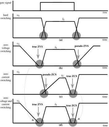
Power semiconductor device commutation can be grouped into two techniques: hard and soft. With hard switching, the devices are required to change their states (on and off), while they are subjected at both finite current and voltage values. High switching stresses pro-duced by the overlapping of voltage and current result in high switching losses. To illustrate the hard switching, figure 1(a) shows the switch voltage and current wave-forms. Soft switching techniques aim is to reduce the mentioned overlap between voltage and current during the commutation. Thus it is possible to reduce switching losses, enabling high frequency operation and achieving higher power density, with reduced audible noise, vol-ume and weight of filters, as well as high output voltage quality.
Soft switching techniques can be classified into two groups: zero voltage switching (ZVS) and zero current switching (ZCS) (Hua and Lee, 1995). In the literature, there are a few reviews of soft switching inverters (Bel-lar et alli, 1998; Pickert and Johnson, 1999; Johnson and Pickert, 1999). The most desirable soft switching scheme is that composed by an auxiliary shunt resonant network, which is activated during the main switches commutation interval only. Therefore, the converter op-eration is very resembled to that without the auxiliary circuit.
In the literature, several soft switching techniques have been proposed for PWM inverters, and nearly all of them operate with ZVS. Typical examples are the auxil-iary resonant commutated pole (ARCP) (Bingen, 1985; McMurray, 1989; De Donker and Lyons, 1990), the ZVS (Barbi and Martins, 1991; Katsis et alii, 1997; Yuan and Barbi, 2000; Lai, 1997b; Pinheiro and Hey, 1996) and ZVT (Zero Voltage Transition) (Choi et alii, 2001)
inverters. In these circuits, the auxiliary commutation circuit only helps main switches turn-on, while turn-off losses are reduced by snubber capacitors. Figure 1(b) shows the current and voltage waveforms of a power switch under ZVS. In some ZVS inverters, the load cur-rent charges the snubber capacitors at main switches turn-off, and as results, there is an important depen-dence between the load current value and the conduc-tion time of the main diodes. Moreover, at high power application where minority carrier devices are usually employed, the turn-off losses caused by tail current can-not be totally avoided with ZVS technique (Kutkut et alii, 1995). Minority carrier devices, such as IGBT and MCT, present better performance with zero current switching, which can minimize substantially the turn-off losses mentioned above. Thus, several ZCS techniques applied to PWM inverters, such as ZCT (Zero Current Transition) inverters, have been reported in the litera-ture (Tomasin, 1998; Li et alii, 2000; Li and Lee, 2001). However, main switches turn-on losses and the adverse effects of the main diodes reverse recovery have not yet been not totally solved (Li and Lee, 2001). Moreover, in the ZCT techniques mentioned, the main switches must turn-on at the exact instant that the auxiliary circuit current reaches the output current value. This implies that the main switches command is dependent of the instantaneous value of the output current, resulting in a more complex command circuit. Figure 1(c) shows the ZCS commutation waveforms.
This paper proposes a new auxiliary commutation cell for PWM inverters, denominated Zero Current and Zero Voltage Transition (ZCZVT). This commutation cell al-lows zero current and zero voltage simultaneously, at both turn-on and turn-off of the main switches. The main switches zero current and zero voltage turn-on can reduce significantly the undesired effects of parasitic in-ductances and capacitances related to the circuit layout, while the zero current turn-off can minimize substan-tially the turn-off losses caused by tail current. In addi-tion, since the rates di/dt and dv/dt are reduced, main diodes reverse recovery losses are minimized. Thus, the commutation losses are practically decreased to zero. Additionally, the commutation time is practically in-dependent of the instantaneous output current value, which simplifies the generation of the command signals for the main and auxiliaries switches. To illustrate this class of commutation, the voltage and current wave-forms of a power switch are shown in figure 1(d).
strategy is presented in Section 4. Experimental results obtained from a 1 kW ZCZVT full-bridge IGBT-based inverter are given in Section 5. The last section summa-rizes the conclusions drawn from this investigation.
2
THE ZCZVT COMMUTATION CELL
Figure 2(a) shows the ZCZVT commutation cell applied to a PWM full-bridge DC-AC converter, which operates with bipolar modulation. The proposed commutation cell is a shunt resonant network made-up of two resonant capacitors CR1 and CR2, two resonant inductors LR1 and LR2, and two bi-directional auxiliary switch SA1 -DA1 and SA2-DA2. The auxiliary commutation cell is activated during the switching transitions only.
gate signal
hard switching
time
time
time
time zero
voltage switching
zero current switching
zero voltage and
current switching
vS
iS
time true ZVS
true ZCS pseudo ZVS
true ZVS true ZCS
pseudo ZCS
vS
iS vS
iS
vS
iS
(a)
(d) (b)
(c)
Figure 1: Commutations waveforms.
The proposed commutation technique can be used in three phase circuits, where one commutation cell for each output phase is used. As shown in figure 2(a), the proposed auxiliary circuit is located in parallel with the output filter and the load. Thus, as the ARCP inverter (Lai et alli, 1996; Lai, 1997a), the three phase version of the proposed circuit can be Y or ∆-configured. As the operation of the single phase inverter it can more eas-ily be understood, once less components are involved, in this paper only the ZCZVT PWM full-bridge
DC-SA2
FILTER AND LOAD
E
CR1
LR1
+
SA1
CR2
LR2 D1
DA2
S1
D2
S2
D3
S3
D4
S4
+
ZCZVT commutation cell
DA1
(a)
SA2
E
CR1
LR1
+
SA1
CR2
LR2
DA2
S1
S2
D3
S3
D4
S4
+
ZCZVT commutation cell
Io
D1
D2
DA1
(b)
Figure 2: ZCZVT full-bridge converter.
AC converter operating with bipolar modulation is anal-ysed.
2.1
Principle of Operation
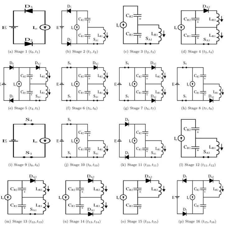
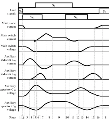
To simplify the analysis, the output current Iois consid-ered constant into one switching cycle. The operation of the auxiliary commutation circuit is symmetrical for the cases of Io<0 and Io>0. So the operation principle will be explained for one case only, i.e., commutations from D2-D3 to S1-S4 and from S1-S4 to D2-D3. As shown in figure 3, there are sixteen operating stages during one switching cycle. These stages are described below:
Stage 1. (t0, t1) Output current Ioflows through main diodes D2 and D3. During this stage the reso-nant capacitors voltages vCR1(t) and vCR2(t) are clamped at –2E and E respectively.
Stage 2. (t1, t2) SA1 is turned on under ZCS at t1. The current through the main diode D2 decreases due to the resonance among LR1, CR1 and CR2. This stage ends when this current reaches zero.
Stage 3. (t2, t3) The output current linearly dis-charges capacitor CR2. The capacitor voltage
D2
D3
Io
E
(a) Stage 1 (t0, t1)
D2 D3 Io E CR2 CR1 SA1 LR1 + +
(b) Stage 2 (t1, t2)
Io CR2 CR1 SA1 LR1 + +
(c) Stage 3 (t2, t3)
DA2 Io CR2 CR1 SA1 LR2 LR1 + +
(d) Stage 4 (t3, t4)
DA2 D1 D4 Io E CR2 CR1 SA1 LR2 LR1 + +
(e) Stage 5 (t4, t5)
DA2 S1 S4 Io E CR2 CR1 SA1 LR2 LR1 + +
(f) Stage 6 (t5, t6)
DA2 S1 S4 Io E CR2 CR1 DA1 LR2 LR1 + +
(g) Stage 7 (t6, t7)
S1 S4 Io E CR2 CR1 DA1 LR1 + +
(h) Stage 8 (t7, t8)
S1
S4
E Io
(i) Stage 9 (t8, t9)
S1 S4 Io E CR2 CR1 SA1 LR1 + +
(j) Stage 10 (t9, t10)
D1 D4 Io E CR2 CR1 SA1 LR1 + +
(k) Stage 11 (t10, t11)
Io CR2 CR1 SA1 LR1 + +
(l) Stage 12 (t11, t12)
DA2 Io CR2 CR1 SA1 LR2 LR1 + +
(m) Stage 13 (t12, t13)
DA2 Io CR2 CR1 DA1 LR2 LR1 + +
(n) Stage 14 (t13, t14)
DA2 Io CR2 CR1 LR2 + +
(o) Stage 15 (t14, t15)
DA2 D2 D3 Io E CR2 CR1 LR2 + +
(p) Stage 16 (t15, t16)
Stage 4. (t3, t4) The resonant capacitor voltages
vCR2(t) vCR1(t) evolve resonantly. When the sum of vCR1(t) and vCR2(t) reaches input voltage, diodes D1 and D4 begin to conduct.
Stage 5. (t4, t5) To assure ZCS and ZVS, main switches S1and S4must be turned-on while D1and D4 are conducting. When the current through D1 and D4 reaches zero, the main switches S1 and S4 begin to conduct.
Stage 6. (t5, t6) The current iLR1(t) decreases and when it reaches zero, the diode DA1begins to con-duct.
Stage 7. (t6, t7) When current iLR2(t) reaches zero, diode DA2 turns off. To assure ZCS and ZVS, the auxiliary switch SA1must be turned off during this stage.
Stage 8. (t7, t8) When current iLR1(t) reaches zero, diode DA1 turns off.
Stage 9. (t8, t9) Operation circuit at this stage is sim-ilar to that of hard-switching PWM full-bridge converter. Output current Io flows through main switches S1 and S4.
Stage 10. (t9, t10) The auxiliary switch SA1 is turned on again under ZCS at t9. The currentiLR1(t) in-creases due to the resonance among LR1, CR1 and CR2. When the current through the main switches S1and S4reaches zero, the diodes D1and D4begin to conduct. The voltage across main switches S1 and S4are clamped at zero.
Stage 11. (t10, t11) The resonance evolves until the current through the main diodes D1and D4reaches zero. To assure ZVS and ZVS, the gate signals of main switches S1 and S4 must be removed during this stage.
Stage 12. (t11, t12) The capacitor CR2 is linearly dis-charged to zero by output current. At this moment diode DA2 begins to conduct.
Stage 13. (t12, t13) The resonant inductor current
iLR1(t) decrease due to the resonance among LR1, LR2, CR1 and CR2. When the current iLR1(t) reaches zero, the diode DA1 begins to conduct.
Stage 14. (t13, t14) The resonance continues. When the current iLR1(t) reaches zero again, the diode DA1is turned off naturally.
Stage 15. (t14, t15) The capacitor CR1 is linearly dis-charged by the output current and the resonant
S2
S1
SA1
1 2 3 4 5 6 7 8 9
Gate signals
Main diode current
Auxiliary
inductor LR1
current Main switch
current
Main switch voltage
Auxiliary
inductor LR2
current
Auxiliary
capacitor CR1
voltage
Auxiliary
capacitor CR2
voltage
Stage
SA1
10 11 12 13 14 15 16 1
S2
Figure 4: Theoretical waveforms.
capacitor voltage vCR2(t) increase due to the res-onance between LR2 and CR2. When the sum of the resonant capacitor voltagesvCR1(t) andvCR2(t) reaches the negative of the input voltage, the diodes D2and D3begin to conduct.
Stage 16. (t15, t0) The resonant inductor current
iLR2(t) decrease due to the resonance among LR2, CR1 and CR2. When the resonant inductor cur-rent iLR2(t) reaches zero the diode DA2 turns off, beginning another switching cycle.
Figure 4 shows the theoretical waveforms of the con-verter operation.
3
RESONANT TANK DESIGN
GUIDE-LINES AND EXAMPLE
This section presents a design procedure and an example to determine the resonant tank elements values of the proposed ZCZVT commutation cell. The given inverter specifications consists of:
Input Voltage E = 200 V
Output Power Po= 1000 W
Output Voltage Vo= 110 Vrms
The design procedure consists of four steps, which are:
a) Find the output current peak from the specifica-tions:
Io=
√
2Po
Vo
(1 + ∆I) (1)
b) Determine the characteristic impedance. To assure main switches turn-off under ZCS and ZVS, during stages 10 and 11, the current peak diverted from main switch to auxiliary circuit must be larger than the output current peak. From these stages, the current peak through capacitor CR2 is given by:
Ipk=
E √
2Z. (2)
By equations (1) and (2), a parameter k can be defined as follows:
k=Ipk
Io
, where k≥1. (3)
By using equations (2) and (3), the characteristic impedanceZ can be defined as:
Z =√E
2kIo
. (4)
c) Determine the resonant frequency. To minimize main diodes reverse recovery, resonant frequency of stage 2 can be chosen to control the di/dt during turn-off. The di/dt of main diodes at stage 2 can be approximate by:
di dt ≈
Ioω
√
2asin1 2k
. (5)
By using equation (5), the resonant frequencyωcan be obtained as follows:
ω= di dt
√
2asin1 2k
Io
. (6)
d) Compute the tank resonant components values. From equations (4) and (6), the resonant compo-nents values can be defined as follows:
LR1=LR2=
Z ω =
E
2kdtdiasin1 2k
, (7)
CR1=CR2= 1
Z·ω =
kI2 o
Edtdiasin1 2k
. (8)
By equations (7) and (8), choosingk= 1.1, which is a practical design value to compensate parasitic
EPLD EPROM
IGBT Drivers Full-Bridge
(Inverter)
Output Filtering
Output Power
Input Power
Pos_Neg
PWM
Figure 5: Block diagram of the command and power circuits.
PWM
SA1
S1
TURN-OFF
TURN-ON
S2
Figure 6: Command circuit waveforms.
losses, and adopting adi/dt of 80 A/µs (Jovanovic and Jang, 2000), the resonant components values can be calculated:
LR1=LR2=
Z
ω = 2.4µH, (9)
CR1=CR2= 1
Z·ω = 34.7nF. (10)
4
COMMAND CIRCUIT STRATEGY
Table 1: Utilized Components and Parameters
Component Parameter
Vin(input voltage) 200 V
LR1 and LR2 2.5µH
CR1 and CR2 33 nF
L (output filter) 500µH C (output filter) 4µF
R (load) 12 Ω
iS2
vS2 I
o
iS2
vS2 Io
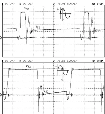
Figure 7: Main switch S2 voltage and current. (scales: 50 V/div.; 10A/div.; 5ms/div.)
where the PWM signal is recorded, and an Erasable Pro-grammable Logic Device (EPLD). The simplicity and programmability of the EPLD make it a good choice for prototyping digital systems. With the PWM and the output current direction, the gate signals are generated in the EPLD. Figure 6 shows the PWM and the gate signals generated in the command circuit represented in figure 5 for Io >0. For Io <0, the main switches gate signals are swapped, and auxiliary switch SA2 is used instead of SA1. As the commutation time is practically independent of the instantaneous output current value, the auxiliary switches conduction times and the delay times between the gate signals of the main and auxil-iary switches are constant.
5
EXPERIMENTAL RESULTS
Following the design example shown in the preceding section, a full-bridge inverter laboratory prototype has been implemented to verify the operation of the pro-posed ZCZVT commutation cell. The power stage cir-cuit is shown in figure 2(a), and the components and parameters used are summarized in Table I. The ac-tive switches were implemented with an UFS (ultrafast switches) series IGBTs from Intersil Semiconductors, which present built-in antiparallel hyperfast diodes. The open-loop command circuit has been implemented using
i
SA1v
SA1Figure 8: Auxiliary switch SA1 voltage and current. (scales: 100 V/div.; 25A/div.; 1ms/div.)
i
LR1-v
CR1Figure 9: Resonant elements waveforms (iLR1(t) and -vCR1(t)). (scales: 100 V/div.; 25A/div.; 1ms/div.)
i
LR1v
CR2v
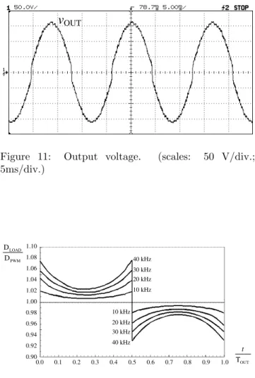
OUTFigure 11: Output voltage. (scales: 50 V/div.; 5ms/div.)
PWM LOAD
D D
OUT
T
t
0.0 0.1 0.2 0.3 0.4 0.5 0.6 0.7 0.8 0.9 1.0 0.90
1.10
1.08
1.06
1.04
1.02
1.00
0.98
0.96
0.94
0.92
40 kHz
30 kHz 20 kHz
10 kHz
10 kHz
20 kHz 30 kHz
40 kHz
Figure 12: Variation of duty-cycle over an output volt-age period.
conventional reference
vREF
OUT
T
t
0.0 0.1 0.2 0.3 0.4 0.5 0.6 0.7 0.8 0.9 1.0
-200 200 160 120 80 40 0 -40 -80 -120 -160
modified reference
Figure 13: Reference signals.
a single EPLD EPM7128SLC84-15 from Altera Corpo-ration.
Figures 7, 8, 9, 10 and 11 show the experimental wave-forms obtained at full load. They confirm the analy-sis made in Section 2. As can be seen in figure 7, the commutations of the main switchesoccurs truly without losses, i.e., with ZCZVS for full load range. This is a very interesting feature introduced by the ZCZVT com-mutation cell. Due to the sloweddi/dt, main diodes re-verse recovery losses are negligible. Figure 8 shows zero current switching of the auxiliary switch SA1. Figures 9 and 10 show the waveforms of the resonant elements.
Figure 11 shows the output voltage of the converter. As can be seen, there is a distortion in the output voltage waveform, where close to zero crossing is observed. This distortion occurs because the converter output voltage stays with the same polarity even after the PWM sig-nal to have changed, and is a consequence of the ac-tion of the auxiliary commutaac-tion cell. Thus, the load duty cycle (DLOAD) is not equal to the PWM duty cy-cle (DP W M). This distortion always occurs either when a commutation cell is inserted in the circuit, or when a dead time is added between the command signals of the switches. In the literature, there is no references describ-ing this effect caused by the use of commutation cells. Dodson et alli (1990) revise the origin of the distortion caused by the dead time, as well as present forms to at-tenuate it. Figure 12 shows the variation of duty cycle of ZCZVT converter over the output voltage period. As can be seen, the relationship between the load duty cy-cle and the PWM duty cycy-cle is directly proportional to the switching frequency of the converter.
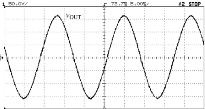
To compensate the variation in the modulation due to the action of the auxiliary commutation cell, a modi-fied PWM signal was generated. Figure 13 shows the conventional reference signal together with the modified signal. These reference signals are for amplitude modu-lation ratio of 0.778 and a switching frequency of 30 kHz. Figure 14 shows the output voltage obtained with the ZCZVT full bridge converter operating with the modi-fied PWM signal. Alternatively, the output voltage dis-tortion can be solved with a closed loop operation.
character-vOUT
Figure 14: Output voltage.(scales: 50 V/div.; 5ms/div.)
90 92 94 96 98 100
250 400 550 700 850 1000
Output Power (W)
Efficiency (%)
Figure 15: Efficiency curve.◦ Hard version;• Soft ver-sion
istic is because the energy involved with the commuta-tion cell is practically constant over all the output power range.
6
CONCLUSIONS
This paper proposes a new ZCZVT full-bridge bipo-lar PWM inverter. Operating principles have been de-scribed and verified by experimental results obtained from a 30 kHz laboratory prototype rated at 1 kW, input voltage of 200V and output voltage of 110Vrms. The experimental results demonstrate that the design pro-cedure proposed is adequate, guaranteeing the correct converter operation.
Soft switching for all power semiconductor devices is achieved. The main switches commutate under ZCS and ZVS simultaneously at both turn-on and turn-off. This commutation technique is therefore suitable for both mi-nority and majority carrier semiconductor device ap-plications such as Power MOSFETs, IGBTs, MCTs, Thyristors etc. In addition, the auxiliary switches com-mutate under ZCS at turn-on and under ZCS and ZVS at turn-off and the main diodes are commutated under ZVS.
The ZCZVT commutation cell is placed out of the main power path of the converters and is activated during the switching transitions only. Additionally, the auxiliary switches use the same ground signal of the upper main switches, and the converter operates with slowdi/dtand dv/dt on power devices, reducing the circuitry noises, and parasitic oscillations.
ACKNOWLEDGMENT
The authors would like to express their special thanks
toIcotron – an EPCOS Company for material support.
REFERENCES
Barbi, I. and D. C. Martins (1991). A true PWM zero-voltage switching pole with very low additional RMS current stress. IEEE Power Electronics
Spe-cialist Conference, pp. 261-267.
Bellar, M. D., T. S. Wu, A. Tchamdjou, J. Mahdavi and M. Ehsani (1998). A review of soft-switched dc-ac converters. IEEE Transactions on Industry
Applications, Vol. 34, No. 4, pp. 847-860.
Confer-ence on Power Electronics and Applications, Vol. 1, pp. 1.15-1.20.
Choi, J. Y., D. Boroyevich, J. Francis and F. C. Lee (2001). A novel ZVT inverter with simplified auxil-iary circuit.IEEE Applied Power Electronics
Con-ference, pp. 1151-1157.
De Donker, R. W. and J. P. Lyons (1990). The auxil-iary resonant commutated pole converter.IEEE
In-dustry Applications Society Annual Meeting Record,
pp. 1228-1235.
Dodson, R. C., P. D. Evans, H. T. Yazdi and S. C. Harley (1990). Compensation for dead time degradation of PWM inverter waveforms.IEE Proceedings B –
Electric Power Applications, Vol. 137, No. 2, pp.
73-81.
Hua, G. and F. C. Lee (1995). Soft-switching techniques in PWM converters. IEEE Transactions on
Indus-trial Electronics, Vol. 42, No. 6, pp. 595-603.
Johnson, C. M. and V. Pickert (1999). Three-phase soft-switching voltage source converters for motor drives. Part 2: Fundamental limitations and criti-cal assessment.IEE Proceedings B – Electric Power
Applications, Vol. 146, No. 2, pp. 155-162.
Jovanovic, M. M. and Y. Jang (2000). A novel ac-tive snubber for high-power boost converters.IEEE
Transactions on Power Electronics, Vol. 15, No. 2,
pp. 278-284.
Katsis, D. C., M. A. Herwald, J.-Y. Choi, D. Boroyevich and F. C. Lee (1997). Drive cycle evaluation of a soft-switched electric vehicle inverter.Annual
Con-ference of the IEEE Industrial Electronics Society,
pp. 658-663.
Kutkut, N. H.; D. M. Divan, D. W. Novotny and R. Marison (1995). Design considerations and topol-ogy selection for a 120 kW IGBT converter for EV fast charging. IEEE Power Electronics Specialist
Conference, pp. 238-244.
Lai, J. S., R. W. Young, G. W. Ott, J. W. McKeever and F. Z. Peng (1996). A delta configured auxiliary resonant snubber inverter. IEEE Transactions on
Industry Applications, Vol. 32, No. 3, pp. 518-525.
Lai, J. S. (1997a). Fundamentals of a new family of aux-iliary resonant snubber inverters. Annual
Confer-ence of the IEEE Industrial Electronics Society, pp.
645-650.
Lai, J. S. (1997b). Resonant snubber-based soft-switching inverters for electric propulsion drives”,
IEEE Transactions on Industrial Electronics, Vol.
44, No. 6, pp.71-80.
Li, Y. and F. C. Lee (2001). A comparative study of a family of zero-current-transition schemes for three-phase inverter applications. IEEE Applied Power
Electronics Conference, pp. 1158-1164.
Li, Yong, F. C. Lee, J. S. Lai and D. Boroyevich (2000). A novel three-phase zero-current-transition and quasi-zero-voltage-transition (ZCT-QZVT) in-verter/rectifier with reduced stresses on devices and components.IEEE Applied Power Electronics
Con-ference, pp. 1030-1036.
McMurray, W. (1989). Resonant snubbers with auxil-iary switches. IEEE Industry Applications Society
Annual Meeting Record, pp. 829-834.
Pickert, V. and C. M. Johnson (1999). Three-phase soft-switching voltage source converters for motor drives. Part 1: Overview and analysis. IEE
Pro-ceedings B – Electric Power Applications, Vol. 146,
No. 2, pp. 147-154.
Pinheiro, J. R. and H. L. Hey (1996). An active auxil-iary commutation circuit for inverters.IEEE Power
Electronics Specialists Conference, pp. 223-229.
Tomasin, P. (1998). A novel topology of zero-current-switching voltage-source PWM inverter for high-power applications. IEEE Transactions on Power
Electronics, Vol. 13, No. 1, pp. 186-193.
Yuan, X. and I. Barbi (2000). Analysis, designing, and experimentation of a transformer-assisted PWM zero-voltage switching pole inverter. IEEE
Trans-actions on Power Electronics, Vol. 15, No. 1, pp.