www.irf.com
1
Note 1: Sinusoidal Modulation at V+=400V, TJ=150°C, FPWM=20kHz, Modulation Depth=0.8, PF=0.6, See Figure 3.
Note 2: tP<100ms; TC=25°C; FPWM=20kHz. Limited by IBUS-ITRIP, see Table "Inverter Section Electrical Characteristics"
Absolute Maximum Ratings
Parameter
Description
Units
V
CES/ V
RRMIGBT/Diode Blocking Voltage
V
V
+Positive Bus Input Voltage
I
O@ T
C=25°C
RMS Phase Current (Note 1)
I
O@ T
C=100°C
RMS Phase Current (Note 1)
A
I
OPulsed RMS Phase Current (Note 2)
F
PWMPWM Carrier Frequency
kHz
P
DPower dissipation per IGBT @ TC =25°C
W
V
ISOIsolation Voltage (1min)
V
RMST
J(IGBT & Diodes)
Operating Junction temperature Range
°C
T
J(Driver IC)
Operating Junction temperature Range
T
Mounting torque Range (M3 screw)
Nm
Values
5
15
20
450
600
10
0.5 to 1.0
27
-40 to +150
2000
I nternal Electrical Schematic - I RAMS10UP60B
23 VS1 24 HO1 25 VB1 1 VCC 2 HIN1 3 HIN2 4 HIN3 5 LIN1
LIN2 6
LIN3 7
F 8
ITRIP 9
EN 10
RCIN 11
VSS 12
COM 13 22
VB2 21 HO2
20 VS2
19 VB3
18 HO3
17 VS3
V- (12)
VB1 (7) U, VS1 (8)
VB2 (4) V, VS2 (5)
VB3 (1) W, VS3 (2)
VCC (14)
VSS (23)
Driver IC
LO1 16
LO3 14 LO2 15
ITRIP (22)
HIN1 (15) HIN2 (16) HIN3 (17)
LIN1 (18) LIN2 (19) LIN3 (20) V (10)+
VTH (13) THERMISTOR
Absolute Maximum Ratings ( Continued)
Symbol Paramet er Min Max Unit s
IBDF
Bootstrap Diode Peak Forward
Current --- 4.5 A
PBR Peak Bootstrap Resistor Peak Power
(Single Pulse) --- 80 W
VS1,2,3
High side floating supply offset
voltage VB1,2,3 - 25 VB1,2,3 +0.3 V
VB1,2,3 High side floating supply voltage -0.3 600 V
VCC
Low Side and logic fixed supply
voltage -0.3 20 V
VIN, VEN, VITRIP Input voltage LIN, HIN, EN, ITrip -0.3
Lower of (VSS+15V) or
VCC+0.3V
V
Condit ions
tP= 10ms,
TJ = 150°C, TC=100°C
tP=100µs, TC =100°C
ESR / ERJ series
I nverter Section Electrical Characteristics @T
J= 25°C
Symbol Parameter Min Typ Max Units
V(BR)CES Collector-to-Emitter Breakdown
Voltage 600 --- --- V
∆V(BR)CES / ∆T
Temperature Coefficient of
Breakdown Voltage --- 0.57 --- V/°C
--- 1.70 2.00
--- 2.00 2.40
--- 5 80 VIN=5V, V+=600V
--- 10 --- VIN=5V, V+=600V, TJ=150°C
--- 1.80 2.35
--- 1.30 1.70 IC=5A, TJ=150°C
-- -- 1.25
--- --- 1.10
RBR Bootstrap Resistor Value --- 2 --- Ω ∆RBR/RBR Bootstrap Resistor Tolerance --- --- ±5 %
IBUS_TRIP Current Protection Threshold
(positive going) 13.1 --- 16.4 A
Condit ions
ICES Zero Gate Voltage Collector
Current µA
VCE(ON) Collector-to-Emitter Saturation
Voltage V
VIN=5V, IC=1.0mA
(25°C - 150°C)
TJ=-40°C to 125°C
See fig. 2 VIN=5V, IC=250µA
V
VBDFM Bootstrap Diode Forward Voltage
Drop V
VFM Diode Forward Voltage Drop
IC=5A, VCC=15V, TJ=150°C
IC=5A, VCC=15V
TJ=25°C
TJ=25°C
IC=5A
IF=1A
I nverter Section Sw itching Characteristics @ T
J= 25°C
Symbol Parameter Min Typ Max Units
EON Turn-On Switching Loss --- 200 235
EOFF Turn-Off Switching Loss --- 75 100
ETOT Total Switching Loss --- 275 335
EREC Diode Reverse Recovery energy --- 15 25
tRR Diode Reverse Recovery time --- 70 100 ns
EON Turn-On Switching Loss --- 300 360
EOFF Turn-off Switching Loss --- 135 165
ETOT Total Switching Loss --- 435 525
EREC Diode Reverse Recovery energy --- 30 40
tRR Diode Reverse Recovery time --- 100 145 ns
QG Turn-On IGBT Gate Charge --- 29 44 nC
RBSOA Reverse Bias Safe Operating Area
SCSOA Short Circuit Safe Operating Area 10 --- --- µs
ICSC Short Circuit Collector Current --- 47 --- A
TJ=150°C, VP=600V,
V+= 360V,
VCC=+15V to 0V See CT2
TJ=150°C, VP=600V, tSC<10µs
V+= 360V, VGE=15V
VCC=+15V to 0V See CT2
FULL SQUARE
Conditions
IC=5A, V+=400V
VCC=15V, L=2mH
Energy losses include "tail" and diode reverse recovery
See CT1
IC=5A, V+=400V
VCC=15V, L=2mH, TJ=150°C
Energy losses include "tail" and diode reverse recovery
See CT1 µJ
µJ
IC=15A, V+=400V, VGE=15V
TJ=150°C, IC=5A, VP=600V
V+= 450V
VCC=+15V to 0V See CT3
Recommended Operating Conditions Driver Function
Symbol Definition Min Max Units
VB1,2,3 High side floating supply voltage VS+12 VS+20
VS1,2,3 High side floating supply offset voltage Note 4 450
VCC Low side and logic fixed supply voltage 12 20
VITRIP ITRIP input voltage VSS VSS+5
VIN Logic input voltage LIN, HIN VSS VSS+5 V
VEN Logic input voltage EN VSS VSS+5 V
Note 3: For more details, see IR21363 data sheet
The Input/Output logic timing diagram is shown in Figure 1. For proper operation the device should be used within the recommende conditions. All voltages are absolute referenced to COM/ITRIP. The VS offset is tested with all supplies biased
at 15V differential (Note 3)
V
V
Note 4: Logic operational for Vs from COM-5V to COM+600V. Logic state held for Vs from COM-5V to COM-VBS.
Static Electrical Characteristics Driver Function
Symbol Definition Min Typ Max Units
VINH ,VENH Logic "0" input voltage 3.0 --- --- V
VINL ,VENL Logic "1" input voltage --- --- 0.8 V
VCCUV+, VBSUV+ VCC and VBS supply undervoltage Positive going threshold 10.6 11.1 11.6 V
VCCUV-, VBSUV- VCC and VBS supply undervoltage Negative going threshold 10.4 10.9 11.4 V
VCCUVH, VBSUVH VCC and VBS supply undervoltage lock-out hysteresis --- 0.2 --- V
VIN,Clamp Input Clamp Voltage (HIN, LIN, ITRIP) IIN=10µA 4.9 5.2 5.5 V
IQBS Quiescent VBS supply current VIN=0V --- --- 165 µA
IQCC Quiescent VCC supply current VIN=0V --- --- 3.35 mA
ILK Offset Supply Leakage Current --- --- 60 µA
IIN+, IEN+ Input bias current VIN=5V --- 200 300 µA
IIN-, IEN- Input bias current VIN=0V --- 100 220 µA
ITRIP+ ITRIP bias current VITRIP=5V --- 30 100 µA
ITRIP- ITRIP bias current VITRIP=0V --- 0 1 µA
V(ITRIP) ITRIP threshold Voltage 440 490 540 mV
V(ITRIP, HYS) ITRIP Input Hysteresis --- 70 --- mV
RON,FLT Fault Output ON Resistance --- 50 100 ohm
VBIAS (VCC, VBS1,2,3)=15V, unless otherwise specified. The VIN and IIN parameters are referenced to COM/ITRIP and are
applicable to all six channels. (Note 3)
Dynamic Electrical Characteristics
Driver only timing unless otherwise specified.)
Symbol Parameter Min Typ Max Units Conditions
TON Input to Output propagation
turn-on delay time (see fig.11) --- 590 --- ns
TOFF
Input to Output propagation
turn-off delay time (see fig. 11) --- 700 --- ns
TFLIN Input Filter time (HIN, LIN) 100 200 --- ns VIN=0 & VIN=5V
TBLT-Trip ITRIP Blancking Time 100 150 ns VIN=0 & VIN=5V
DT Dead Time (VBS=VDD=15V) 220 290 360 ns VBS=VCC=15V
MT Matching Propagation Delay Time
(On & Off) --- 40 75 ns
VCC= VBS= 15V, external dead
time> 400ns
TITrip
ITrip to six switch to turn-off
propagation delay (see fig. 2) --- --- 1.75 µs VCC=VBS= 15V, IC=10A, V
+
=400V
--- 7.7 --- TC = 25°C
--- 6.7 --- TC = 100°C
VCC=VBS= 15V, IC=10A, V+=400V
Post ITrip to six switch to turn-off
clear time (see fig. 2)
I nput- Output Logic Level Table
FLT- EN
I
TRIPHIN1,2,3 LIN1,2,3
U,V,W
1
0
0
1
V
+1
0
1
0
0
1
0
1
1
Off
1
1
X
X
Off
0
X
X
X
Off
Ho
Lo
U,V,W
IC Driver
V+
Hin1,2,3
Lin1,2,3 (15,16,17)
(18,19,20)
(8,5,2)
Thermal and Mechanical Characteristics
Symbol Paramet er Min Typ Max Unit s Condit ions
Rth(J-C) Thermal resistance, per IGBT --- 4.2 4.7
Rth(J-C) Thermal resistance, per Diode --- 5.5 6.5
Rth(C-S) Thermal resistance, C-S --- 0.1
---CD Creepage Distance 3.2 --- --- mm See outline Drawings
°C/W
Flat, greased surface. Heatsink compound thermal conductivity 1W/mK
I nternal NTC - Thermistor Characteristics
Parameter Definition Min Typ Max Units Conditions
R25 Resistance 97 100 103 kΩ TC = 25°C
R125 Resistance 2.25 2.52 2.80 kΩ TC = 125°C
B B-constant (25-50°C) 4165 4250 4335 k R2 = R1e [B(1/T2 - 1/T1)]
Temperature Range -40 125 °C
Typ. Dissipation constant 1 mW/°C TC = 25°C
I nternal Current Sensing Resistor - Shunt Characteristics
Symbol Paramet er Min Typ Max Unit s Condit ions
RShunt Resistance 33.0 33.3 33.7 mΩ TC = 25°C
TCoeff Temperature Coefficient 0 --- 200 ppm/°C
PShunt Power Dissipation --- --- 2.2
W
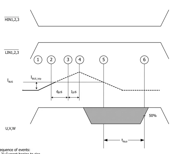
-40°C< TC <100°CLIN1,2,3 HIN1,2,3
tfltclr
50%
U,V,W
IBUS_trip
6µs 1µs
IBUS
Sequence of events: 1-2) Current begins to rise
2) Current reaches IBUS_Trip level
2-3) Current is higher than IBUS_Trip for at least 6µs. This value is the worst-case condition with very low
over-current. In case of high current (short circuit), the actual delay will be smaller. 3-4) Delay between driver identification of over-current condition and disabling of all outputs 4) Current starts decreasing, eventually reaching 0
5) Current goes below IBUS_trip, the driver starts its auto-reset sequence
6) Driver is automatically reset and normal operation can resume (over-current condition must be removed by the time the drivers automatically resets itself)
3
4
2
1
5
6
Note 5: The shaded area indicates that both high-side and low-side switches are off and therefore the half-bridge output voltage would be determined by the direction of current flow in the load.
Module Pin- Out Description
1
23
Pin Name Descript ion
1 VB3 High Side Floating Supply Voltage 3
2 W,VS3 Output 3 - High Side Floating Supply Offset Voltage
3 NA none
4 VB2 High Side Floating Supply voltage 2
5 V,VS2 Output 2 - High Side Floating Supply Offset Voltage
6 NA none
7 VB1 High Side Floating Supply voltage 1
8 U, VS1 Output 1 - High Side Floating Supply Offset Voltage
9 NA none
10 V+ Positive Bus Input Voltage
11 NA none
12 V- Negative Bus Input Voltage
13 VTH Temperature Feedback
14 VCC +15V Main Supply
15 HIN1 Logic Input High Side Gate Driver - Phase 1
16 HIN2 Logic Input High Side Gate Driver - Phase 2
17 HIN3 Logic Input High Side Gate Driver - Phase 3
18 LIN1 Logic Input Low Side Gate Driver - Phase 1
19 LIN2 Logic Input Low Side Gate Driver - Phase 2
20 LIN3 Logic Input Low Side Gate Driver - Phase 3
21 FLT/Enable Fault Output and Enable Pin
22 ITRIP Current Sense and Itrip Pin
Typical Application Connection I RAMS10UP60B
1. Electrolytic bus capacitors should be mounted as close to the module bus terminals as possible to reduce ringing and EMI problems. Additional high frequency ceramic capacitor mounted close to the module pins will further improve perfor-mance.
2. In order to provide good decoupling between VCC-VSS and VB1,2,3-VS1,2,3 terminals, the capacitors shown connected be-tween these terminals should be located very close to the module pins. Additional high frequency capacitors, typically 0.1µF, are strongly recommended.
3. Value of the boot-strap capacitors depends upon the switching frequency. Their selection should be made based on IR design tip DN 98-2a, application note AN-1044 or Figure 9. Bootstrap capacitor value must be selected to limit the power dissipation of the internal resistor in series with the VCC. (see maximum ratings Table on page 3).
4. Current sense signal can be obtained from pin 22 and pin 23. Care should be taken to avoid having inverter current flowing through pin 22 to mantain required current measurement accuracy.
5. After approx. 8ms the FAULT is reset. (see Dynamic Characteristics Table on page 5).
6. PWM generator must be disabled within Fault duration to garantee shutdown of the system, overcurrent condition must be cleared before resuming operation.
7.Fault/Enable pin must be pulled-up to +5V.
HIN2 HIN3 LIN1 LIN2 LIN3 HIN1 D a te C o d e L o t #
2
3
IR
A
M
S
1
0
U
P
6
0
B
1
3-Phase AC MOTOR BOOT-STRAP CAPACITORS U V WVcc(15 V)
Figure 3. Maximum Sinusoidal Phase Current vs. PWM Switching Frequency
V
+=400V , T
J
=150°C, Modulation Depth=0.8, PF=0.6
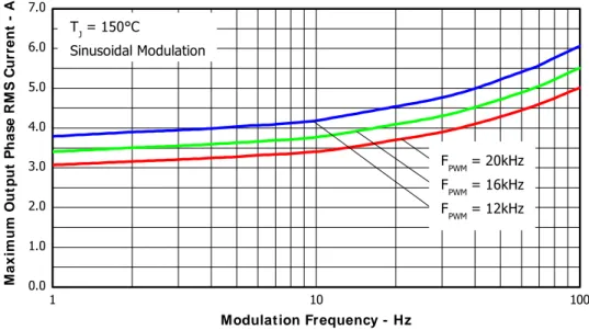
Figure 4. Maximum Sinusoidal Phase Current vs. Modulation Frequency
V
+=400V, T
J
=150°C, T
C=100°C, Modulation Depth=0.8, PF=0.6
1 10 100
0.0 1.0 2.0 3.0 4.0 5.0 6.0 7.0
TJ = 150°C
Sinusoidal Modulation M a x im u m O u tp u t P h a s e R M S C u rr e n t - A
Modulation Frequency - Hz
FPWM = 20kHz
FPWM = 16kHz
FPWM = 12kHz
0 2 4 6 8 10 12 14 16 18 20
0.0 1.0 2.0 3.0 4.0 5.0 6.0 7.0 8.0
TJ = 150°C
Sinusoidal Modulation M a x im u m O u tp u t P h a s e R M S C u rr e n t - A
PW M Frequency - kHz
TC = 100°C
TC = 110°C
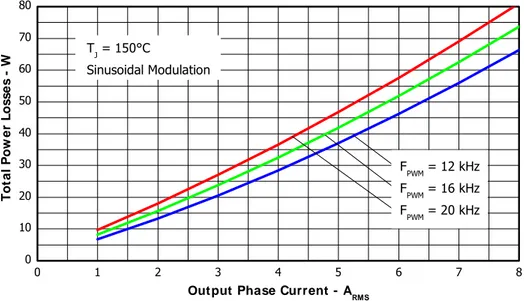
Figure 5. Total Power Losses vs. PWM Switching Frequency, Sinusoidal modulation
V
+=400V , T
J
=150°C, Modulation Depth=0.8, PF=0.6
Figure 6. Total Power Losses vs. Output Phase Current, Sinusoidal modulation
V
BUS=400V , T
J=150°C,
Modulation Depth=0.8, PF=0.6
0 2 4 6 8 10 12 14 16 18 20
0 10 20 30 40 50 60 70
T
o
ta
l
P
o
w
e
r
L
o
s
s
e
s
W
PW M Sw itching Frequency - kHz
IOUT = 6 ARMS
IOUT = 5 ARMS
IOUT = 4 ARMS
TJ = 150°C
Sinusoidal Modulation
0 1 2 3 4 5 6 7 8
0 10 20 30 40 50 60 70 80
TJ = 150°C
Sinusoidal Modulation
T
o
ta
l
P
o
w
e
r
L
o
s
s
e
s
W
Output Phase Current - ARMS
FPWM = 12 kHz
FPWM = 16 kHz
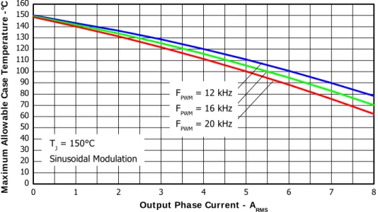
Figure 7. Maximum Allowable Case temperature vs. Output RMS Current per Phase
Figure 8. Estimated Maximum IGBT Junction Temperature vs. Thermistor Temperature
0 1 2 3 4 5 6 7 8
0 10 20 30 40 50 60 70 80 90 100 110 120 130 140 150 160 T
J = 150°C
Sinusoidal Modulation M a x im u m A ll o w a b le C a s e T e m p e ra tu re -°C
Output Phase Current - ARMS
FPWM = 12 kHz
FPWM = 16 kHz
FPWM = 20 kHz
65 70 75 80 85 90 95 100 105 110 115
100 110 120 130 140 150 160
T
Javg. = 1.2363 x T
Therm+ 26.2775
I G B T J u n c ti o n T e m p e ra tu re ° C
Figure 10. Recommended Bootstrap Capacitor Value vs. Switching Frequency
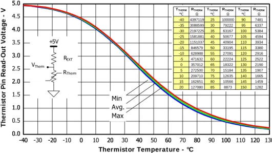
Figure 9. Thermistor Readout vs. Temperature (47kohm pull-up resistor, 5V) and
Nominal Thermistor Resistance values vs. Temperature Table.
0 5 10 15 20
1.0 2.0 3.0 4.0 5.0 6.0 7.0 8.0 9.0 10.0 11.0 12.0 13.0 14.0 15.0 16.0 3.3µF 6.8µF RBS
DBS CBS RG1 RG2 VS HO LO COM vB VCC HIN LIN +15V VSS V+ HIN LIN U,V,W GND VSS 2.2µF 4.7µF R e c o m m e n d e d B o o ts tr a p C a p a c it o r - µ F
PW M Frequency - kHz 15µF
-40
-40 -30 -20-20 -10 00 10 2020 30 4040 50 6060 70 8080 90 100100 110 120120 130 0.0 0.0 0.5 1.0 1.0 1.5 2.0 2.0 2.5 3.0 3.0 3.5 4.0 4.0 4.5 5.0 5.0 +5V VTherm RTherm REXT T h e rm is to r P in R e a d -O u t V o lt a g e V
Thermistor Temperature - °C
Min Avg. Max
TTHERM RTHERM TTHERM RTHERM TTHERM RTHERM
°C Ω °C Ω °C Ω
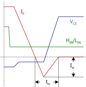
Figure 11. Switching Parameter Definitions
Figure 11a. Input to Output Propagation
turn-on Delay Time
Figure 11b. Input to Output Propagation
turn-off Delay Time
Figure 11c. Diode Reverse Recovery
50% HIN/LIN
V
CEI
CH
IN/L
INT
OFFt
f 90% IC10% IC
50% VCE
V
CEI
CH
IN/L
INT
ONt
r 50%HIN/LIN 90% IC
10% IC
50% VCE
V
CEI
FH
IN/L
INt
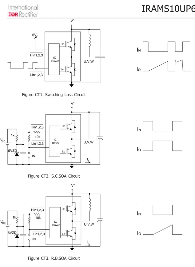
rrFigure CT1. Switching Loss Circuit
Figure CT2. S.C.SOA Circuit
Figure CT3. R.B.SOA Circuit
HoLo
U,V,W
IC Driver
Lin1,2,3 5V
Hin1,2,3
Ho
Lo
U,V,W
IC Driver
V+
Lin1,2,3 Hin1,2,3
IN 10k 1k
5VZD VCC
Io
Ho
Lo
U,V,W
IC Driver
V+
Lin1,2,3 Hin1,2,3
IN 10k 1k
5VZD VCC
Io
I
NI
OI
NI
OI
NStandard pin leadforming option
Notes:
Dimensions in mm
1- Marking for pin 1 identification
2- Product Part Number
3- Lot and Date code marking
4-
Tollerances
±0.5mm, unless otherwise stated
For mounting instruction, see AN1049
027-E2D24IRAMS10UP60B
note 1
note 2
Data and Specifications are subject to change without notice
I R W ORLD HEADQUARTERS:
233 Kansas St., El Segundo, California 90245, USA Tel: (310) 252-7105
TAC Fax: (310) 252-7903
Visit us at www.irf.com for sales contact information
01/08
Package Outline
For mounting instruction see AN-1049
Pin leadforming option -2
Notes:
Dimensions in mm
1- Marking for pin 1 identification
2- Product Part Number
3- Lot and Date code marking
4-
Tollerances
±0.5mm, unless otherwise stated
027-E2D24
note 1
IRAMS10UP60B-2