Available Techniques for Magnetic Hard Disk Drive
Read Channel Equalization
Nuno Miguel de Figueiredo Garrido
Instituto Universitário de Lisboa (ISCTE-IUL)Instituto de Telecomunicações (IT-IUL) Lisboa, Portugal
+351 - 217 903 984
[email protected]
ABSTRACT
This paper presents an extensive, non-exhaustive, study of available hard disk drive read-channel equalization techniques used in the storage and readback of magnetically stored information. The physical elements and basic principles of the storage processes are introduced together with the basic theoretical definitions and models. Both read and write processes in magnetic storage are explained along with the definition of simple key concepts such as user bit density, intersymbol interference, linear and areal density, read head pulse response models, and coding algorithms. The building blocks of disk drive electronics are succinctly described. The main read channel architectures: partial-response maximum likelihood (PRML) and Decision Feedback Equalization (DFE) based systems, are described and compared. Two continuous-time practical solutions are presented for the forward equalizer (the critical block of the system) in the MDFEs architecture. Recursive adaptive continuous-time filters based on gm-C topology are proposed for the implementation of the equalizer. An orthonormal state-space recursive current mode filter is proposed and compared at transistor level to a companion-form canonical structure. The basic circuits for the implementation of building blocks are presented and compared to existing solutions. A self-biased transconductance cell is presented for the implementation of very high frequency current mode gm-C filters using biased MOSFET capacitor arrays in standard digital CMOS technology.
1. BASIC PRICIPLES OF MAGNETIC
HARD DISK DRIVE SYSTEMS
Magnetic support has long been the prime choice for non-volatile data storage. The physical characteristics of magnetic disk devices are a fine match for the requirements of fast and non-sequential recording and playback of digitally stored data, pushing its performance way beyond its magnetic storage counterparts in all relevant parameters. Mass production of desktop and laptop computers has quickly led magnetic disks from 3.5” multi-disk bays to single-platter 2.5”, 1.8” or even 0.85” disk drives with the traditional architecture scaled to fit a thumbnail, defying even the obvious appeal of massive non-volatile solid state disks (SSD) or flash memories.
Hard disk drives (HDD) store data by magnetizing a thin 10–30 nm ferromagnetic film coating on an endurable physical foothold, usually a platter made of aluminium alloy or glass/ceramics. The
1 The tracks are further divided in angle defined portions called
sectors, each having data and header servo fields for correct track positioning and monitoring, gain setting and clock recovery.
magnetic tracks on the media surface are narrow concentric rows of very small magnets containing user information. Earlier designs using magnetic film surface veneers can easily fit several thousand circular concentric tracks1 per centimetre (or up to a million in later
and more advanced designs). A conventional track can pack more than 200 kbit per inch in slight individual magnetic records (linear bit density) or up to 1 Mbit per inch for perpendicular to platter recording. Each of these magnetic dipoles are used to hold and playback non-volatile data.
The user bit2 is recorded on the disk surface driven by a magnetic
flux throughput imposed on the magnetic head during the write process. Once stored on these tiny independently oriented magnets, the bit can be sensed during playback as a very low amplitude3
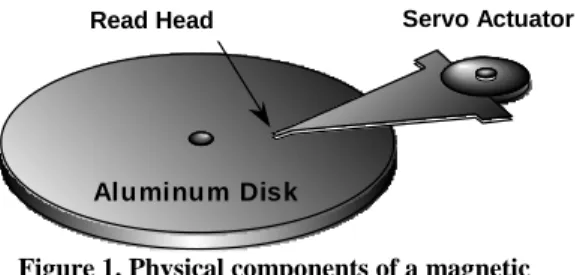
voltage pulse that is subsequently processed and transmitted by the read circuitry back to the data bus via the host interface controller. Regardless of its size, the basic physical components of a magnetic disk storage apparatus are depicted in figure 1. A magnetic disk device mainly consists of four basic physical components: spindle motor, platter (the aluminium disk), servo actuator, and read head.
Figure 1. Physical components of a magnetic hard disk drive storage system
HDDs usually have two electric motors: one for the spindle, and the other serving as a servo actuator for the read head arm. The spindle motor is used to steer the movement of the disk(s), spinning its angular velocity up to more than 10000 revolutions per minute (rpm) for high performance disks, and is accountable for about 40% of the total disk drive power. The head actuator or servo actuator arm, is responsible for the accurate positioning of the magnetic head over a random track on the disk. The inductive head hovers over the surface of the disk, at the end of the actuator arm. It is usually made of a microscopic magneto-sensitive alloy embraced by a coiled wire.
2 Logical 1 if there is a transition on flux magnetization (either left
to right or right to left) and logical 0 if no transition occurs.
3 The raw output pulses induced on the read head have
approximately 1mVpp.
Aluminum Disk
Actuactor Inductive HeadRead Head Servo Actuator
Older disk systems used conventional inductive C-shaped or metal in gap (MIG) read heads in which the flux flows parallel to the film coating on the disk surface. The use of magnetoresistance (MR) and giant magnetoresistance (GMR), and of thin film read heads optimized and further separated the read and write process, but only with the introduction of tunnelling magnetoresistance (TMR) and perpendicular magnetic recording (PMR) in 2005, the orientation of the flux from the read head changed from parallel to perpendicular to the film coating thus allowing even tighter magnetic packing up to 1Tbit per square inch (areal density). Even though this has major implications to the write process, especially to the head structure and magnetic disk media, it has no significant impact on the read process, neither on the read sensor nor on the read channel.
1.1 Disk-drive electronic blocks
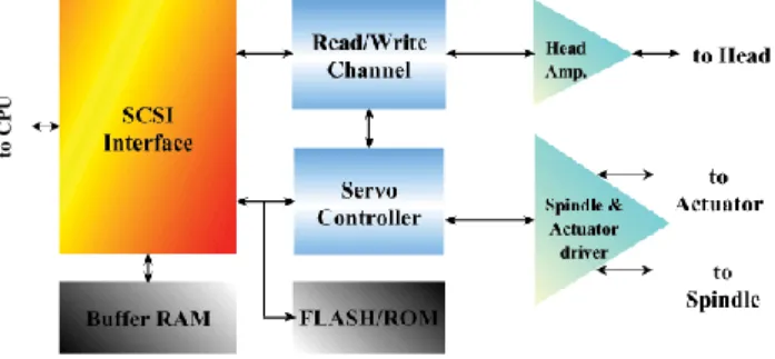
The read/write process is long and complex, starting out on the CPU all the way to the media magnets and vice versa, several electronic blocks are necessary to assure proper bit detection. Figure 2 depicts the functional diagram of all the electronic blocks involved in most disk drive system architectures.
Figure 2. Physical components of a magnetic disk drive storage system
The basic building blocks are the host interface DSP4, the
read/write channel and the servo controller5. These blocks are
usually assisted by a head amplifier6, and by a spindle and actuator
motor driver7 front-end IC, along with some auxiliary elements for
non-volatile and short-term memory. Consistent endeavour for cheaper solutions in the last decade have reduced the number of required integrated circuits from a dozen components including ASICs to just three or four ICs, corresponding to the functional blocks.
The read/write channel is the fundamental mixed signal analog/digital block of HDD electronics and is composed of two separate channels: the read channel extracts the clock, equalizes de input read head pulse, makes the digital decision and decodes data; the write channel basically encodes data. This work is focused on
4 The host interface is a digital IC that controls the data interface
between the read/write channel and the CPU, handling interrupts, and data transfer protocols common to magnetic or solid-state drives. Auxiliary buffer RAM is used for caching and queuing data, providing long data-bursts to improve speed and reduce bus latency.
5 The servo DSP calculates actuator trajectories and controls the
spindle and actuator driver to correctly position and maintain the read head on track.
6 The head pre-amplifier is a 40dB gain wideband single chip
device usually mounted close to the read head, driving the head
the read channel, and particularly, on its key component, the pulse-slimming equalizer. The equalizing target of the system is strongly dependent on the magnetic head response, and hence, on the physical properties of the playback and write processes.
1.2 Playback process
The playback process is usually originally initiated by the CPU and issued onto the disk electronic blocks through a SCSI or IDE bus controller IC. The host interface controller forwards the order to the servo controller, which in turn positions the head actuator onto the designated track, according to the track ID stored on the servo sectors. Once the head is in a fixed position, the rotating movement of the disk allows that the read channel IC can correctly access and feedback the stored user data to the host interface controller8.
The relative movement of the stored magnets on the disk’s surface in respect to the read head causes a variation of the magnetic flux that flows through the head core. The changes in the direction of magnetization represent encoded binary data bits, hence the variation in time of the magnetic flux density flow through an electric circuit wire loop coiled on the read head generates an electric field, as results from Faraday’s law expressed in its integral form by
dt d t
v()
. (1)The properties of the communication channel, including read head characteristics and the physical ground rules of the read/write process can be treated as reasonably linear and time invariant. Therefore, a proper linear time-invariant system can be used to model the physical medium of the channel. The step response of the read back procedure is easy to extract based upon measured data from a specific physical medium to a stored positive transition, i.e. a specific head and media can be fully characterized from the analysis of a single flux transition.
1.2.1 Read head model
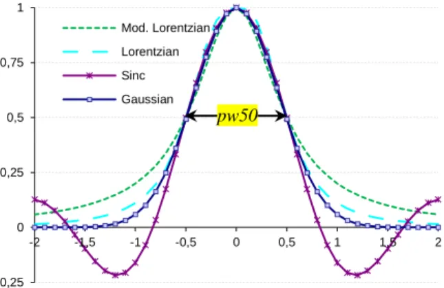
The Lorentzian model is the most widely used step response model of the playback process in recording systems. The commonly used equation for the Lorentzian pulse model shown in (2) is a good approximation for most of the referred magnetic read heads response to a positive transition in magnetic flux polarity.
2 50 2 1 1 ) ( pw t t s (2) The model is normalized to unitary peak value, and constant pw50 denotes the pulse width at 50% of its peak value. The corresponding pulse is depicted in figure 3, along with other common pulse shapes often used in signal processing, such as sinc, Gaussian or modified
during the write process and amplifying the input pulse during the read process, yielding approximately 25dB of SNR.
7 The spindle and actuator driver is a power IC responsible for
driving the head actuator and the spindle motor, it is usually implemented with power CMOS, and its consumption is about 10% of the total power needs.
8 The elapsed time between data request and data ready at the bus
is defined as the access time of the disk, usually in the order of 10 to 20 milliseconds. In most cases, the host interface controller buffers the read data in local memory, before sending it back to the host processor. This is also usually combined with sophisticated software disk caching schemes.
to
CP
Lorentzian. In this model, t=0 corresponds to the instant that the read head hoverflies the boundary region of two adjacent magnets of opposite polarities, and hence, for maximum efficiency, most read channel architectures use clock recovery schemes to precisely sample and decide at this instant.
Figure 3. Read head pulse model (Lorentzian) The portion of the response obtained for negative instants (precursor) reflects the physical fact that the influence of flux transition is sensed by the read head before it actually reaches the transition boundary, thus, since this effect precedes the optimum sampling instant, it effectively corresponds to a prior awareness of a future event, and therefore is inherently non-causal. This portion of the response is usually referred to as precursor response. Likewise, the postcursor response designates the part of the pulse that follows the transition instant. The superimposition of two consecutive flux transitions denoting consecutive ones, usually designated as dipulse or dibit response, represents the effect of allowing Inter Symbolic Interference (ISI) to occur between adjacent bits, and is frequently used to characterize the response of the read channel.
These physical constrains together with the thrust for slimmer pulses determine the dimensions of the head and justify their fabrication process, but the growing need for higher data storage densities and increased data rates have forced the use of complex circuitry systems to compensate for the amount of allowed ISI. User bit density (UBD) is defined as the pw50/T ratio, where T denotes time (or distance) between consecutive bits. High-speed acquisition and sharpening of the magnetic-head data input-pulses, is done mainly at the expense of high silicon area (thus high cost) and (unfortunately) high power consumption especially on high frequency channels. However, very slim digital bits allowing huge areal density are the essence of mass data storage, hence, different techniques are employed in data coding for the achievement of optimal performance either in data rate, error probability, noise immunity and ISI forbearance. Several coding procedures and data constrains have been used (and even combined) in magnetic read
9 The d constrain • minimum run-length constrain, imposes that
transitions between different symbols occur at least d+1 apart from each other.
The k constrain • maximum run-length constrain, imposes that a transition between different symbols occurs at most k symbols after the previous one.
10 NRZI coding codes zeros as no-transition and ones as sign-transitions, only a long series of zeros would inevitably lead
to the loss of synchronism. A limitation must be imposed on the
channels as a result of this effort, and the read channel topology greatly depends on the chosen coding strategy as will be shown.
1.2.2 Coding techniques
One of the most common coding schemes widely employed in data coding, especially in optical and magnetic recording is Run-Length Limitation (RLL). This coding technique9 is characterized by two
integer constrains (d,k). The d constrain avoids consecutive transitions between different symbols, thus assuring at least d+1 consecutive zeros or ones when a transition occurs. This constrain reduces the maximum bit rate and storage capacity, but allows the increase of the operating frequency whilst dropping speed requirements for crucial circuit blocks. The use of RLL (1,7) became typical in disk drive systems although it reduces user data rate to 2/3, since it maps 2 bits on to 3 bits. The k constrain avoids long unvarying sequences of consecutive zeros or consecutive ones, that can lead to the loss of synchronism between the clock recovery circuitry driving the detection block and the transmitted data. This is a typical problem of asynchronous data transmission systems10 and usually has little influence on data rate.
1.3 Write process
The write process is also triggered when the host interface controller receives an order from the host processor, commanding that a given data sequence is stored onto the disk. Typically, some or all of the data will be transferred in advance, packed into blocks and buffered locally. As described for the read process, the servo controller as to position the head actuator onto a designated track. Once the head is in position, the write bits are forwarded to the write channel where they are encoded and output via the magnetic head driver to the head, through which they are forced onto the rotating disk11.
The basic principal behind non-volatile recording of a bit on the surface of a magnetic disk is the establishment of a magnetic field imposed by an electric current flow through an electric wire. The fundamental law relating magnetic field strength and electric currents is the well-known Biot-Savart law. The current flow on the wire coiled around the magnetic head generates a magnetic field. Assuming a saturation recording system, the magnetic flux is proportional to the write current as given by
I
L
. (3)As the magnetic field is forced onto and through the disk surface, it is enduringly stored as magnetically oriented magnets with negative or positive polarity depending on the value of the stored
allowed length between ones, therefore at most k consecutive zeros can occur. In any case consecutive sequences of ones are not tolerable in NRZI coding due the d constrain.
11 The physical constrains determining the access time during the
write procedure are similar to the referred for the playback process. Access time can be up to 100 times smaller in solid state disks when compared with magnetic HDD, but these can cost 10 times more. -0,25 0 0,25 0,5 0,75 1 -2 -1,5 -1 -0,5 0 0,5 1 1,5 2 Mod. Lorentzian Lorentzian Sinc Gaussian pw50
bit. The value of the magnetic flux density 𝐵⃗ vector can be precisely imposed on the ferromagnetic layer, and can be derived from
SdS
N
B
. (4)For enhanced behavior some systems include a non-linear distortion at the beginning of the current pulse during the write process. This is meant to increase the initial slope of the stored pulse, thus accounting for a significant reduction of non-causal intersymbol interference. This technique is designated as write pre-compensation. This can considerably alter the pulse shape displacing signal power from the beginning of the pulse to the pulse center, and pulse tail, thus it can slightly increase causal intersymbol interference that can be in term compensated using appropriate filtering.
2. STATE OF THE ART OF READ
CHANNEL ARCHITECTURES
The first solutions in magnetic hard disk drive storage for personal computers were proposed in 1980 closely followed by the first 3 ½" floppy drives in 1981. Early designs used conventional peak-detection read channels, basically relying on the zero crossing of the differentiated input signal, to sample the input at its local minimum or maximum value. These designs have gradually evolved to present days, and now usually include equalizer blocks with high frequency boost for pulse-slimming and more complex clock recovery schemes. Nevertheless, more advanced read channel architectures based on partial-response and more recently DFE based systems have taken the place of peak detection techniques.
2.1 Peak detection read channels
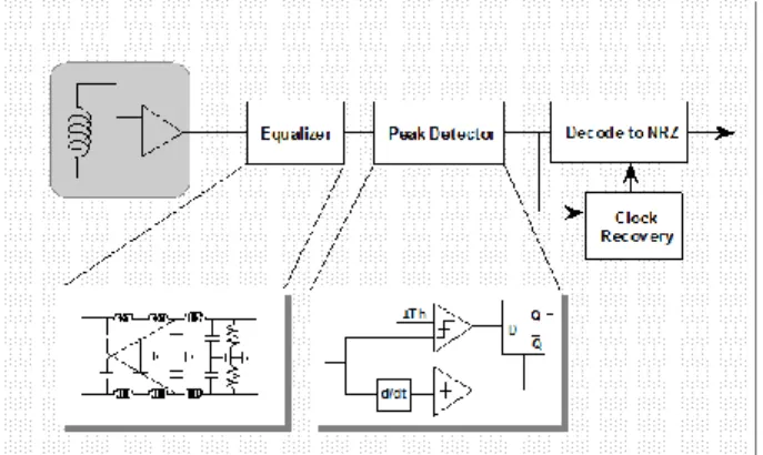
Peak detection has been the conventional technique for data acquisition, and the main market solution for several decades for the read channel since the appearance of disk drives. This scheme combines the lowest implementation cost with high efficiency in RLL encoded channels, especially for low-density disks. The peak-detector block depicted in figure 4 is the key functional block of this read channel.
This block differentiates the input signal from the read head amplifier, and uses a simple comparator set to ground, thus identifying zero crossing. The output of the comparator clocks a flip-flop circuit ideally sampling the input signal at its local minimum or maximum value, the sampling instant is centered on the timing window with acceptably high accuracy and noise immunity. A peak is detected if the module of the input value is greater than a threshold voltage (usually half the maximum amplitude), thus corresponding to a recorded symbol “1”, otherwise
the output of the detector will yield the symbol “0”. The equalizer block is usually a wideband high-order passive differential low-pass filter used as a pulse-slimming equalization filter for improved performance, it usually combines high-frequency boost with low noise enhancement. The clock recovery and decoder blocks synchronize and decode the user data.
The main features of this scheme are simplicity, low power and low complexity. The main limitation of peak detection read channels is that the data-encoding scheme doesn’t allow the use of more aggressive data storage techniques based on the augment of user bit density. This limitation in linear data density strongly compromises the desired storage capacities, whilst maintaining slow data transfer speeds. As data density increases, the flux reversals are packed more tightly and start to interfere with each other, whereas these analog peaks are processed at higher rates, thus significant overlapping occurs, leading to inter-symbolic interference and to data bit errors, timing errors, peak shifts, peak drops. All of these can contribute significantly for the reduction of bit error rates (BER). To reduce interference whilst augmenting bit-density, the magnetic fields must decrease, thus peak detection becomes a week solution, especially at user bit densities pw50/T superior to 1. This has made alternative read channel schemes flourish, and proved them superior to traditional peek detection read channels. To solve this problem, IBM introduced its first-generation partial-response maximum likelihood (PRML) read channel technology in hard disk-drives in 1990. The PRML approach differs from traditional peak detector read channels, which do not compensate for ISI, by using advanced digital filtering processing to shape the read signal frequency and timing characteristics to a desired partial response, and by using maximum-likelihood digital data detection to determine the most likely sequence of data bits that was written to the disk.
2.2 Partial response maximum likelihood
read channels
Partial Response Maximum Likelihood (PRML) coding in magnetic recording was first proposed by Kobayashi et al. [1-2] early in 1970 based on Lender’s work on correlative level coding [3]. However, only recently has it been monolithically implemented. The main features of PRML are the modeling of the read channel as a linear finite-state machine and the use of maximum likelihood decoding as proposed by Viterby [4], thus allowing increased data rates and user bit density, and hence, augmented disk storage capacity when compared with standard non-return-to-zero (NRZ) and RLL coding peak detection read channels. This performance is achieved with additional complexity and high consumption especially at high data rates. Different classes of partial response read channels [5-10] share the same simplified structure depicted in figure 5.
Figure 5. Partial response read channel block diagram It includes an analog to digital converter (ADC), a digital finite impulse response (FIR) adaptive equalizer, and a Maximum Likelihood Sequence Detector (MLSD), usually a Viterbi algorithm detector is used as an efficient approach to MLSD. Later designs have also included a discrete time FIR forward equalizer Figure 4. Peak detection read channel block diagram
after the low-pass filter for precursor ISI removal. The clock recovery circuitry provides the desired sampling rate and phase for the sample and hold block at the ADC input, based on a feedback loop filter and on a Voltage Controlled Oscillator (VCO). The keys to this scheme are fast analog to digital and efficient ISI cancelling on the adaptive equalizer.
The referred partial response (PR) coding is done in the adaptive equalizer, the key block of the read channel. Different approaches to the coding are available although all of them are based on the partial response polynomial shown in (5).
(5) This delay polynomial derives from the z-transform of the equalizer function where D = z -1, and the equalizer complexity is given by
number of tapped delays and equal to m + n. The differentiating function of the read head on the NRZ pattern is usually given by (1-D) thus most PR schemes use m=1. Coefficients m and n determine the complexity of the equalizer transfer function each corresponding to a variant of PR as shown in table 1.
Table 1. Partial response variants
m n Coding
1 0 No coding NRZI
0 2 Class II Partial Response PR2 1 1 Class IV Partial Response PR4 1 2 Class IV Extended Partial Response EPR4 1 3 Class IV Extended Partial Response E2PR4
2.2.1 Partial response class IV
All partial response read channels assume a fixed well-known model for the read head response to an isolated transition and linear superposition of adjacent transitions. Partial response coding based on m=1 and n=1, denominated Class IV or simply PR4, is a simple and elegant realization of PR, where each voltage pulse results in two samples, thus delaying the decision in time, as given by PR polynomial 2 1 ) 1 ( ) 1 ( ) (D D D D P . (6)
In the late nineties several PRML-based solutions for the read channel were proposed [11-18] all employing advanced and aggressive analog to digital converters, allowing areal densities to increase by up to 50% when compared to conventional peak detection channels. Greater overall capacities and faster transfer bit rates rapidly pushed these read channels as the new standard for data decoding on modern hard disks. Extended versions of PRML with longer partial response polynomials, such as EPRML and E2PRML, using much more complex implementations of the
maximum likelihood algorithm, also became available.
2.2.2 Extended partial response class IV
An improved solution using m=1 but setting n=2 further extends the response in time, given that each isolated pulse results in a sequence of three voltage samples (1,2,1) as a consequence of the quadratic form of term (1+D)2 on equation (5). This PRML codding
12 Consumption and area values for ADC only [26].
technique is designated as extended partial response Class IV, or EPR4 and is given by equation
3 2 2 1 ) 1 ( ) 1 ( ) (D D D D D D P . (7)
The use of a better algorithm and more complex signal-processing allowed a more than 20% increase in linear density, and hence in areal density, without increasing BER. Further development of PR class IV using m=1 and n=3 as given by
4 3 3 2 2 1 ) 1 ( ) 1 ( ) (D D D D D D P (8)
has been proposed and several viable solutions [19-27] have been presented to implement the read channel. Read channels using this coding scheme, designated as E2PRML or E2PR4, have allowed the
augment of total disk capacity, and consequently have been widely adopted in the hard disk industry replacing PRML. E2PR4 systems
can also take advantage of density gains and combine RLL(1,7) encoding with non-return-to-zero inverted (NRZI) modulation. Several PR employing d=0 run length constraint have also been presented to reduce the complexity of the detector whilst attaining higher code rates. E2PRML equalisation can reduce critical
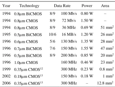
requirements such as high frequency, although extended PRML schemes increase circuit complexity and require higher resolution for the ADC. Fast suboptimal simplified Viterbi detectors are usually used since the complexity of MLSD increases exponentially with the number of tapped delays. Unfortunately, high transfer rates imply costly consumption requirements since power consumption in digital blocks is roughly proportional to the signal frequency, and hence to the data transfer rate, this is particularly important in the case of portable systems where power consumption is the key to balance speed and battery operation autonomy. Table 2 summarizes the most relevant characteristics of proposed PRML read channels showing the available results for data rate, power consumption, die area and technology.
Table 2. PRML channel evolution
Year Technology Data Rate Power Area 1994 0.8m BiCMOS 8/9 100 Mb/s 0.80 W – 1994 0.8m CMOS 8/9 72 Mb/s 1.50 W – 1994 0.8m CMOS 8/9 36 MHz 0.69 W 51 mm2 1995 0.5m BiCMOS 10/6 16 MB/s 1.20 W 26 mm2 1996 0.6m CMOS 5/6 130 Mb/s 1.35 W 28 mm2 1996 0.7m BiCMOS 7/6 150 Mb/s 1.55 W 47 mm2 1996 0.5m BiCMOS 8/9 200 Mb/s 0.85 W 20 mm2 1996 1.0m CMOS 160 MHz 0.46 W 23 mm2 1999 0.35m CMOS12 300 MHz 0.23 W 0.8 mm2 2002 0.18m CMOS13 150 Mb/s 0.18 W 1 mm2 2006 0.35m CMOS13 300 MHz – 12.8 mm2
Various magnetic read-channels based on PRML have been able to meet the increase of data acquisition rates. However, this has been accomplished at the expense of complexity and power dissipation. Performance limitations of PRML solutions based on fast ADC acquisition and bulky signal processing leave short margin for data
13 Proposed for optical disc formats, CD, DVD and Blu-ray disk
(BD) in [27].
rate increases, thus strongly limiting their application in HDD read channels, although still showing to be robust solutions for optical data systems such as DVD/Blu-ray.
Alternative architecture delivering equivalent performance to the most advanced partial response read channel solutions, were presented based on decision feedback equalization (DFE) using digital FIR filter techniques that avoid high frequency acquisition ADC. In August 1996, Philips Semiconductors announced its first standard RAM-DFE read channel device, a fully-adapted self-training DFE scheme compatible with a wide range of read head and media interfaces. Adaptation allows improved bit-error rate achieving signal-to-noise ratio equivalent to PR4 read channel, at increased user data bit density (superior to 2.0).
2.3 Decision feedback equalization
read channels
The Decision Feedback Equalization (DFE) structure was first presented in 1967, by M. Austin as an equalizing technique for dispersive channels, as described in [28]. Adaption capability was further proposed and added to the system in 1971 by D. George et
al. in [29], but it was only in 1996 that this scheme was firstly
integrated in a commercial circuit as a practical alternative to peak detection techniques. This is also the main structure from which derived some of the schemes described onward (such as FDTS/DF, RAM-DFE and MDFE). It basically consists of two equalizing filters and a decision element (slicer) as depicted in figure 6.
The forward equalizer is typically a linear FIR filter used for precursor ISI cancellation and the backward equalizer is a non-linear postcursor ISI remover. The non-non-linearity in the feedback caused by the decision element ideally enhances noise robustness, although once an error occurs it will propagate to subsequent symbols. One interesting feature of this equalization scheme is the possibility to tune both filter sections. This is usually accomplished using LMS modified algorithms. Consequently tapped delay transversal FIR filters are the natural choice for these blocks due to their ease of implementation and tuning or programming abilities.
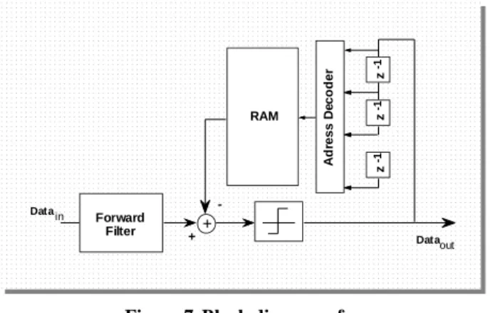
2.3.3 RAM decision feedback equalization channel
RAM-based equalization is also used for ISI removal on storage channels, although it was first presented as a non-linear echo canceller for data modems [30]. This technique is particularly effective on channels for which the linear superposition is an inaccurate model. The non-linear effects on postcursor ISI can be canceled by detecting the sequence of the previous symbols and subtracting the corresponding RAM-stored value (for that particular sequence) from the signal at the input of the slicer. The detected sequence is temporarily stored in a shift-register whose outputs decode the RAM element that holds the expected error values, as depicted on figure 7. The stored values can/must be tuned recursively to improve equalizing performance although this can prove to have convergence problems and comparatively higher
complexity then adaptive linear equalizers. The forward filter is a linear equalizer, usually a FIR filter as those used in conventional DFE read channels.
Figure 7. Block diagram of a RAM-based decision feedback read channel
In linear echo cancellation, the assumption for canceling causal ISI using linear equalizers is that a linear superposition of the previously detected symbols will model the total echo on the current symbol. This principle suggests the use of transversal FIR filters for this purpose as was described previously. Alternatively non-linear cancellation as proposed by Agazzi et al. [31] assumes echo signals to be a non-linear function of the current and past symbols, requiring the channel to be time invariant, and also suggesting the use of memory elements. The first DFE equalizer using RAM-Based equalization was published in 1989 by Fisher et
al [32-33] but its hardware complexity as kept it away from the
disk-drive market, moreover with the high linearity behavior of magneto resistive read heads at high densities. Nevertheless, a publication by Sands et al. [34] reporting a 200 MHz RAM-DFE channel using a linear adaptive tapped delay forward filter and a non-linear adaptive backward equalizer comprising a RAM element and a linear adaptive equalizer led to the launch of a standard RAM-DFE read channel by Philips in 1996. In a later publication Brown and Hurst [35] propose a complete RAM-DFE chip with 11.2 mm2 operating at 80 Mb/s and dissipating 630 mW
using a first order continuous-time forward equalizer and a 4-tap FIR backward equalizer.
2.3.4 Fixed-delay tree search with decision feedback
channel
The Fixed-Delay Tree Search with Decision Feedback (FDTS/DF) equalizer was first presented in 1988, by J. Moon and L. Carley [36-38] as a quasi-optimum implementation of a Maximum-Likelihood Sequence Detector (MLSD) for Run-Length-Limited (RLL) with a decision element similar to partial response. The equalizer basically consists on a forward and a backward filter, along with a FTDS decision block. Usually a FIR filter is used as a forward equalizer to cancel the precursor ISI, although adaptive analog implementations can lower the power consumption needs. Causal ISI is eliminated using a feedback filter as in DFE, but the weights of the feedback taps are smaller than its DFE counterparts thus reducing error propagation. The complete block diagram is depicted in figure 8 including the LMS algorithm block used to make the forward equalizer adaptive.
Dataout Forward Equalizer Data in + + -Backward Equalizer Dataout Forward Filter Datain + + -RAM A d re s s D e c o d e r -1z z -1 z -1
Figure 6. Decision feedback equalization block diagram .
Figure 8. Block diagram of a
Fixed Delay Tree Search with decision feedback read channel. The decision delay goal is to look ahead some symbols before making the decision, according to an exhaustive tree-search, as the one shown in figure 9. Similarly to a Viterbi detector, the most likely path (or sequence) is determined by minimizing the Euclidean distance between predictable and detected sequences.
Figure 9. Binary tree search structure
The FTDS algorithm achieves near-optimum performance in the case of RLL constrained input sequences since the critical error events are short and invalid paths are of easy detection, making it of reasonable hardware complexity and cost, with a performance close to that of MLSD. The d constrain in RLL (1,7) code significantly reduces the number of possible paths and the complexity of the decision tree. Moreover, low-end drives have prompted considerable efforts for the development of low power continuous-time adaptive equalizer solutions alternative to the digital FIR approach usually used with DFE read channels. Several studies [39-42] led to the proposal of Multilevel Decision Feedback Equalization (MDFE), and in February 1995, Kenney suggested the development of an allpass continuous-time filter solution for the realization of the forward equalizer with equivalent performance to that of a long tapped-delay FIR filter as the key block of MDFE.
2.3.5 Multilevel decision feedback equalization
channel
Multilevel Decision Feedback Equalization was first presented in 1993, by Kenney et al [43-45] as a quasi-optimum implementation of a Maximum-Likelihood Sequence Detector (MLSD) for Run-Length-Limited (RLL) systems. The block diagram of MDFE
14 SC-FIR denotes discrete time FIR tapped delay filter using
switched-capacitor delay cells.
A-FIR denotes discrete time FIR tapped delay filter using gm-C or OTA-C to implement the delay cells.
depicted in figure 10 is similar to that of FTDS/DF, also comprising a forward and a backward filter, but using a simple slicer instead of a FTDS decision block, just like the other DFE-based systems. However, this results from the simplification of the FTDS decision block, providing the channel uses RLL (1,7) encoded data.
Figure 10. Block diagram of a Multilevel Decision Feedback Equalization
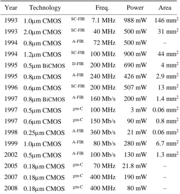
Usually a FIR filter is used as a forward equalizer to cancel the non-causal precursor ISI, but [46] suggests that an adaptive analog implementation can show equivalent performance to that of a long (24 taps) FIR filter, whilst decreasing power consumption needs. Causal ISI is eliminated using an equalizing filter in the feedback loop, just as in DFE but also with reduced weights of the feedback taps. Table 3 comprises several equalizers proposed for implementation the forward equalizer in PRML and DFE read channels.
Table 3. Equalizer evolution14
Year Technology Freq. Power Area 1993 1.0m CMOS SC-FIR 7.1 MHz 988 mW 146 mm2 1993 2.0m CMOS SC-FIR 40 MHz 500 mW 31 mm2 1994 0.8m CMOS A-FIR 72 MHz 500 mW – 1994 1.2m CMOS SC-FIR 100 MHz 900 mW 44 mm2 1995 0.5m BiCMOS D-FIR 200 MHz 690 mW 4 mm2 1995 0.8m CMOS A-FIR 240 MHz 426 mW 2.9 mm2 1996 0.6m CMOS SC-FIR 200 MHz 507 mW 13 mm2 1997 0.8m BiCMOS A-FIR 160 Mb/s 200 mW 1.4 mm2 1997 0.5m CMOS gm-C 100 MHz 3 mW 0.06 mm2 1997 0.6m CMOS gm-C 150 Mb/s 90 mW 0.8 mm2 1998 0.25m CMOS A-FIR 360 Mb/s 21 mW 0.06 mm2 1999 1.0m CMOS A-FIR 80 Mb/s 280 mW 6.7 mm2 2002 0.5m CMOS A-FIR 100 Mb/s 130 mW 1.3 mm2 2005 0.18m CMOS gm-C 70 MHz 21.8 mW – 2007 0.18m CMOS gm-C 400 MHz 190 mW – 2008 0.18m CMOS gm-C 400 MHz 80 mW –
D-FIR denotes discrete time digital FIR filter. gm-C denotes continuous time gm-C filter.
Cited equalizers [57-73] use different filtering techniques.
+ -Forward Equalizer Backward Equalizer ek
It is of considerable interest that both filters operate in current-mode so that the outputs of these filters are added in the current summing node that precedes the sampling switch. The adaptation process depends on the generation of the error signal estimated by the difference between the prediction value at the input of the slicer and the data decision at its output.
For the implementation of a 3rd order allpass continuous-time adaptive equalizer [47-49], designed to work at very high frequency at low power consumption - less than one tenth of traditional FIR power needs - and low supply voltage, the design option was to use adaptive state-space recursive filters based on current-mode Gm-C structures employing low-mismatch high bandwidth pseudo-differential balanced transconductors and polarized MOSFET arrays as integrating capacitors.
3. AVAILABLE TECHNIQUES FOR THE
EQUALIZER
A previous theoretical work [46] based on MATLAB simulation for a 100 MHz sampling frequency can be used to derived ideal pole locations for the forward equalizer. For a third order system, the pole positions maximizing performance can be show to be:
Real Pole f = 8 MHz
Complex Poles f0 = 26 MHz Q = 0.6
and hence, the system transfer function can be expressed by
24 16 2 8 3 24 16 2 8 3 10 3754 . 1 10 1308 . 4 10 26 . 3 10 3754 . 1 10 1308 . 4 10 26 . 3 ) ( S S S S S S s H (9)
3.2 Adaptive Gm-C Architectures
For the above specifications, two Gm-C current-mode structures were designed and compared based on transistor level simulations. Both architectures adapt using LMS modified algorithms [50-56], and allow the parasitic input capacitance in the Gms to be taken into account for very high frequency operation. The automatic tuning of the poles frequency also compensates process tolerances that influence the effective value of the active devices and capacitors. The equalizers linearity is mainly determined by the linearity of the transconductors and integrating capacitors. The DC voltage inherent to the simulated structures biases these transistors well beyond their threshold voltage for enhanced linearity behavior.
2.2.1 Canonical Structure
Firstly, we considered the canonical structure illustrated in figure 11. It is composed of four equal value pseudo-differential transconductors embedded in a grounded capacitive network.
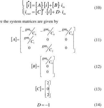
The corresponding 3rd order current mode state-space recursive system can be expressed as
in T out ini
D
i
C
i
i
B
i
A
i
(10)where the system matrices are given by
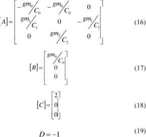
0 0 0 0 2 2 1 1 0 0 0 0 0 0 C gm C gm C gm C gm C gm A (11)
0 0 0 0 C gm B (12)
2 0 2 C (13) 1 D (14)Notice that matrix [A] assumes the typical row-shape characteristic of canonical structures. The system transfer function is thus given by 3 2 2 2 1 2 2 1 0 3 3 2 2 2 1 2 2 1 0 3 ) ( gm gm SC gm C C S C C C S gm gm SC gm C C S C C C S s H (15)
Considering equal-valued transconductors with a nominal transconductance value of 60 S and after subtracting the effect of the parasitic input capacitance of the Gms we obtain the following nominal values for the integrating capacitors
Co = 0.083pF, C1 = 0.47pF, C2 = 1.8pF.
2.2.2 Orthonormal Structure
In alternative to the canonical structure described before we also considered the orthonormal structure represented in figure 12. Although the design of the orthonormal structure is usually a more complex approach, it can take a rather simplified format for the allpass filter. Moreover, it uses only one of the state variables to build the allpass current output wave and thus making it more immune to noise and offset problems than the previous canonical structure. gm gm in V + -+ -+ -+ + -+ - gm + -+ - gm + -+ -+ -+ -+ -+ -+ -+ I I out out gm gm gm gm -+ + + + + + + + - -- - -- - - - -+ +- - + + ++ I I in out out V
Figure 11. Canonical structure .
Figure 12. Orthonormal structure .
The corresponding 3rd order state-space system is also expressed by matrix equation (10) but the system matrices are now given by
0 0 0 0 2 2 1 1 1 1 0 0 0 0 C gm C gm C gm C gm C gm A (16)
0 0 0 0 C gm B (17)
0 0 2 C (18) 1 D (19)A simple scaling of the system state-variables would transform it in the orthonormal ladder structure proposed in [53]. Hence, since the filter satisfies Lyapunov's equation
0 2 T T bb KA AK (20)
all the system state-variables are orthogonal and the dynamic range is optimized. The system transfer function for the structure in Fig. 3 is given by 3 2 2 0 2 1 2 2 1 0 3 3 2 2 0 2 1 2 2 1 0 3 ) ( ) ( ) ( gm gm C C S gm C C S C C C S gm gm C C S gm C C S C C C S s H (21)
Considering again equal-valued transconductors with the same nominal value of 60 S and after subtracting the effect of the input capacitance of the Gms we obtain the following nominal values for the integrating capacitors
C0 = 0.102pF, C1 = 0.49pF, C2 = 1.77pF.
3.3 Adaptive Capacitor Array
The adaptation of the Gm-C filters previously described is achieved by means of integrating capacitor structures Ci consisting of a
constant course MOSFET capacitor Ci' in parallel with an N-bit
digitally controlled fine tuning capacitor array Ci, as shown in
figure 13.
Figure 13. Integrating capacitors are formed by a fixed capacitor in parallel with a digitally controlled
capacitor-array. the total integrating capacitance is given by
Ci = Ci’ + Ci (22) where ik N k ik i C Bit C
0 (23) and iN k ik C C 2 (24)thus can be expressed as
ik N k k iN i C Bit C
0 2 (25)The minimum value Ci’ and the maximum value Ci’ + max(Ci) of
each integrating capacitor Ci are dimensioned to allow the desirable
placement of the poles, even under worst case process tolerances that influence the actual value of Gms and of the integrating capacitors. The number of adaptation bits must provide sufficient adaptation precision of the arrays without unduly increasing the circuit complexity. For both structures described before we considered N = 4-bit capacitor arrays made of biased 12.5 fF unit size transistor cells that can be switched on and off by the adaptive control logic. The adaptation process is assumed to be done during the clock recovery preamble and be stable at the decision instants. Alternatively the capacitor array can be loaded in parallel and subsequently adapted to optimum values.
3.4 Transconductors
The transconductors employed in the above filters are based on balanced pseudo-differential lossy-C structures, as shown in figure 14. Unlike in the circuit used in [57-58], biasing is provided by the feedback loops established in the filter, yielding improved stability and noise immunity. Moreover, the transistors dimensions determining the biasing voltages were calculated to minimize the allowed mismatch while maintaining maximum frequency performance. Computer simulations showed that such transconductors are capable of maintaining the correct operation of the filter for supply voltages as low as 1.8 V.
Figure 14. Balanced pseudo-differential transconductor.
3.5 Results and Discussion
3.5.6 Frequency Response
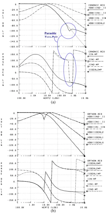
Transistor level simulations of both structures with nominal integrating capacitance values produce the amplitude and phase versus frequency response characteristics shown in figure 15.(a) and figure 15.(b), respectively for the canonical and orthonormal structures. Whereas with the response of the canonical structure there is a parasitic zero-pair mismatch in state variable Iin2 around
450MHz in the orthonormal structure all state variables IIni nearly
match the ideal IIdeali amplitude and phase characteristics well over
Figure 15. Frequency response of the (a) canonical and (b) orthonormal filter structures, for nominal integrating
capacitance values
This shows that under identical design conditions the orthonormal structure has a better high frequency performance behavior. Besides, the orthonormal structure has improved adaptability capabilities since it allows independent pole tuning.
3.5.7 Transient Response
The transient response of both structures was analyzed using an input corresponding to measured data from the magnetic read head. Waveshape Vin represents consecutive transitions, one up and one
down, usually mentioned as dibit response. The resulting equalized transient response of the orthonormal and canonical outputs are
15 Other useful references [74-104]
superimposed and are both represented by Ireal in figure 16, showing
that both structures practically match the predicted response from the ideal implementation IIdeal.
Figure 16. Dibit-response of the allpass filter
4. CONCLUSIONS
This paper presented the most relevant read-channel equalization techniques used in hard disk drive storage. Basic principles and key concepts are introduced along with the building blocks of disk drive electronics. The main read channel architectures alternative to peak-detection: PRML-based and DFE-based are described and compared. Two fully analog continuous-time integrated adaptive filters are proposed for the implementation of an allpass forward equalizer for MDFE read channels. An orthonormal current mode state-space recursive filter is proposed and shown superior at transistor level to a companion-form equivalent canonical structure. Current mode continuous-time gm-C filters using auto-biased transconductance cells operating at very high frequency combined with biased MOSFET capacitor arrays in standard digital CMOS technology are proposed, Operating with supply voltages as low as 1.8 V, whilst reducing consumption by a factor of 10 to 100 compared to conventional FIR digital equalizers exhibiting equivalent performance.
REFERENCES
15[1] H. Kobayashi and D. Tang, “Application of Partial Response Channel Coding to Magnetic Recording Systems”, IBM
Journal of Research and Development, pp. 368-375,
Jul. 1970.
[2] H. Kobayashi, “Correlative level coding and
maximum-likelihood decoding”, IEEE Trans. Information
Theory, vol. IT-17, pp. 586-594, Jul. 1971.
[3] A. Lender, “Correlative level coding for binary-data transmission”, IEEE Trans. on Com., vol. COM-14, pp. 67-70, 1966. Parasitic Zero-Pair (a) . (b) .
[4] A. J. Viterby, “Error bounds for convolutional codes and asymptotically optimum decoding algoritm”, IEEE Trans.
Information Theory, vol. IT-13, pp. 260-269, 1967.
[5] Roger Wood, “New Detector for 1,k Codes Equalized to Class II Partial Response”, IEEE Trans. on Magn., vol. 25, no. 5, pp. 4075-4077, Sept. 1989.
[6] F. Dolivo, R. Hermann and S. Ölçer, “Performance and Sensitivity Analysis of Maximum-Likelihood Sequence Detection on Magnetic Recording Channels”, IEEE
Trans. on Magn., vol. 25, no. 5, pp. 4072-4074, Sept. 1989.
[7] J. D. Coker et al., “Implementation of PRML in a Rigid Disk Drive”, IEEE Trans. on Magn., vol. 27, no. 6, pp. 4538-4543, Nov. 1991.
[8] William L. Abbot, John M. Cioffi and Hemant K. Thapar, “Performance of Digital Magnetic Recording with Equalization and Offtrack Interference”, IEEE Trans. on
Magn., vol. 27, no. 1, pp. 705-716, Jan. 1991.
[9] John Hong, Roger Wood and David Chan, “An Experimental 180 Mb/sec PRML Channel for Magnetic Recording”, IEEE
Trans. on Magn., vol. 27, no. 6, pp. 4532-4537, Sept. 1991.
[10] Gregory T. Uehara and Paul R. Gray, “Parallelism in Analog and Digital PRML Magnetic Disk Read Channel Equalizers”,
IEEE Trans. on Magn., vol. 31, no. 2, Nov. 1994.
[11] Gregory T. Uehara and Paul R. Gray, “A 100MHz Output Rate Analog-to-Digital Interface for PRML Magnetic-Disk Read Channels in 1.2m CMOS”, ISSCC Digest of Tech.
Papers, pp. 280-281, 1994.
[12] William Abbott et al., “A Digital Chip with Adaptive Equalizer for PRML Detection in Hard-Disk Drives”, ISSCC
Digest of Tech. Papers, pp. 284-285, 1994.
[13] R. D. Yamasaki et al., “A 72Mb/s PRML Disk-Drive Channel Chip with an Analog Sampled-Data Signal Processor”, ISSCC Digest of Technical Papers, pp. 278-279, Feb. 1994.
[14] Rick. A. Philphott et al., “A 7Mbyte/s (65MHz), Mixed-Signal, Magnetic Recording Channel DSP Using Partial Response Signaling with Maximum Likelihood Detection”, IEEE J. Solid-State Circuits, vol. 29, no. 3, Mar. 1994.
[15] Jeff Sonntag et al., “A High Speed, Low Power PRML Read Channel Device”, IEEE Trans. on Magn., vol. 31, no. 2, Mar. 1995.
[16] C. Peterson et al., “A 3-5.5V CMOS 32Mb/s Fully-Integrated Read Channel for Disk-Drives”, IEEE Trans. on Magn., vol. 31, no. 2, Mar. 1995.
[17] Raymond Richetta et al., “A 16MB/s PRML Read/Write Data Channel”, ISSCC Digest of Tech. Papers, pp. 78-79, 1995.
[18] K. Parsi et al., “A 200Mb/s PRML Read/Write Channel IC”,
ISSCC Digest of Technical Papers, pp. 66-67, 1996.
[19] Danfeng Xu, Yonghua Song and Gregory T. Uehara, “A 200MHz 9-Tap Analog Equalizer for Magnetic Disk Read Channels in 0.6m CMOS”, ISSCC Digest of Tech. Papers, pp. 74-75, 1996.
[20] Patrick Pai, Anthony Brewster, Asad Abidi, “A 160MHz End IC for EPR-IV PRML Magnetic-Storage Read Channel”
ISSCC Digest of Tech. Papers, pp. 68-69, 1996.
[21] G. Tuttle et al., “A 130 Mb/s PRML Read/Write Channel with Digital-Servo Detection”, ISSCC Digest of Tech.
Papers, pp. 64-65, 1996.
[22] Seiichi Mita et al., “A 150 Mb/s PRML Chip for Magnetic Disk Drives”, ISSCC Digest of Tech. Papers, pp. 62-63, 1996.
[23] Mei-Tjin Huang et al., “A 20MHz BICMOS Peak Detect Pulse Qualifier and Area Detect Servo Demodulator for Hard Disk Drive Servo Loop”, ISSCC Digest of Tech. Papers, pp. 326-327, 1997.
[24] Jon Fields et al., “A 200 Mb/s CMOS EPRML Channel with Integrated Servo Demodulator for Magnetic Hard Disks”,
ISSCC Digest of Tech. Papers, pp. 314-315, 1997.
[25] Roberto Alini et al., “A 200 MSampleb/s Trellis-Coded PRML Read/Write Channel with Digital Servo”, ISSCC
Digest of Tech. Papers, pp. 318-319, 1997.
[26] Mehr, I. and Dalton, D., “A 500-MSample/s, 6-bit
Nyquist-rate ADC for disk-drive read-channel applications”,
IEEE J. Solid-State Circuits, vol.34, no.7, pp. 912-920,
Jul 1999.
[27] Gunjae Koo, “A robust PRML read channel with digital timing recovery for multi-format optical disc”, Proc. IEEE
ISCAS, vol. 4, pp. 21-24, May 2006.
[28] M. E. Austin, “Decision-Feedback Equalization for Digital Communication Over Dispersive Channels”, MIT/RLE, Tech.
Rep. 461, Aug. 11, 1967.
[29] D. A. George, R. R. Bowen and J. R. Storey, “An Adaptive Decision Feedback Equalizer”, IEEE Trans. on Com. Tech., vol. 19, no. 3, pp. 281-293, Jun. 1971.
[30] Gottfried Ungerboeck, “Fractional Tap-Spacing Equalizer and Consequences for Clock Recovery in Data Modems”,
IEEE Trans. on Com., vol. COM-24, no. 8, pp. 856-864,
Aug. 1976.
[31] Oscar Agazzi and David G. Messerschmitt, “Nonlinear Echo Cancellation of Data Signals”, IEEE Trans. on Com., vol. COM-30, no. 11, pp. 2421-2433, Nov. 1982.
[32] K. Fisher, J. Cioffi and C. M. Melas, “An Adaptive DFE for Storage Channels Suffering from Non-linear ISI and Transition Dependent Noise”, ICC 89, Boston, Jun. 1989. [33] K. Fisher, J. Cioffi and C. M. Melas, “An Adaptive
RAM-DFE for Storage Channels”, IEEE Trans. on Com., vol. COM-39, no. 11, pp. 1559-1568, Nov. 1991. [34] Nicholas P. Sands et al., “A 200Mb/s Analog DFE Read
Channel”, ISSCC Digest of Tech. Papers, pp. 72-73, 1996. [35] Brown, J.E.C.; Hurst, P.J.; Rothenberg, B.C.; Lewis, S.H.,
"A CMOS adaptive continuous-time forward equalizer, LPF, and RAM-DFE for magnetic recording," IEEE J. Solid-State
Circuits, vol.34, no.2, pp. 162-169, Feb 1999.
[36] Jackyun J. Moon and L. Richard Carley, “Partial Response Signaling in a Magnetic Recording Channel”, IEEE
Trans. on Magn., vol. 24, no. 6, pp. 2973-2975, Sept. 1988.
[37] Jackyun J. Moon and L. Richard Carley, “Performance Comparison of Detection Methods in Magnetic Recording”,
IEEE Trans. on Magn., vol. 26, no. 6, pp. 3155-3172,
Nov. 1990.
[38] Jaekyun Moon, “Discrete-Time Modeling of Transition-Noise-Dominant Channels and Study of Detection
Performance”, IEEE Trans. on Magn., vol. 27, no. 6, pp. 4573-4578, Nov. 1991.
[39] Arvind M. Patel, “A New Digital Signal Processing Channel for Data Storage Products”, IEEE Trans. on Magn., vol. 27, no. 6, pp. 4579-4584, Nov. 1991.
[40] Jack K. Wolf, “A Survey of Codes for Partial Response Channels”, IEEE Trans. on Magn., vol. 27, no. 6, pp. 4585-4589, Nov. 1991.
[41] Jaekyun Moon and Sian She, “Constrained-Complexity Equalizer Design for Fixed Delay Tree Search with Decision Feedback”, IEEE Trans. on Magn., vol. 30, no. 5, pp. 2762-2768, Sept. 1994.
[42] L. Richard Carley and John G. Kenney, “Comparison of Computationally Efficient Forms of FTDS/DF Against PR4-ML”, IEEE Trans. on Magn., vol. 27, no. 6, pp. 4567-4572, Nov. 1991.
[43] John G. Kenney, L. Richard Carley and Roger W. Wood, “Multi-level Decision Feedback Equalization for Saturation Recording”, IEEE Trans. on Magn., vol. 29, no. 3, pp. 2160-2171, Jul. 1993.
[44] John G. Kenney, “A System Architecture for Multi-level Decision Feedback Equalization”, IEEE Trans. on Magn., vol. 30, no. 6, pp. 4218-4221, Nov. 1994.
[45] John G. Kenney and Roger Wood, “Multi-level Decision Feedback Equalization: An efficient Realization of FDTS/DF”, IEEE Trans. on Magn., vol. 31, no. 2, Mar. 1995.
[46] Peter McEwen and John G. Kenney, “Allpass Forward Equalizer for Decision Feedback Equalization”, IEEE Trans. on Magn., vol. 31, no. 6, pp. 3045 3047, Nov. 1995. [47] Nuno Garrido, J. Franca, and J. Kenney, “A Comparative
Study of Two Adaptive Continuous-Time Filters for Decision Feedback Equalization Read Channels”,
Proc. IEEE ISCAS, vol. 1, pp. 89-92, Jun. 1997.
[48] Nuno de F. Garrido and José E. Franca, “An Auto-Biased 0.5m CMOS Transconductor for Very High Frequency Applications”, Proc. IEEE ISCAS, vol. 1, pp. 325 328, Jun. 1998.
[49] Nuno de F. Garrido and José E. Franca, “A Continuous-Time Area Detector Servo Demodulator for Hard Disk Drives”,
Proc. IEEE ICECS, vol. 2, pp. 127 130, Sept. 1998.
[50] Ayal Shoval, David A. Johns and W. Martin Snelgrove, “Comparison of DC Offset Effects in Four LMS Adaptive Algorithms”, IEEE Trans. Circuits Syst. II, vol. 42, no. 3, Mar. 1995.
[51] David A. Johns, W. Martin Snelgrove and Adel S. Sedra, “Orthonormal Ladder Filters”, IEEE Trans. Circuits Syst., vol. 36, no. 3, pp. 337-343, Mar. 1989.
[52] David A. Johns and Adel S. Sedra, “Synthesis and analyses of State-Space Active Filters Using Intermediate Transfer Function”, IEEE Trans. Circuits Syst., vol. 33, pp. 287-301, Mar. 1986.
[53] K. A. Kozma, David A. Johns and Adel S. Sedra, “An Adaptive Tuning Circuit for Integrated Continuous-Time Filters”, Proc. IEEE ISCAS, pp. 1163-1166, 1990. [54] David A. Johns, W. Martin Snelgrove and Adel S. Sedra,
“Continuous-Time LMS Adaptive Recursive Filters”, IEEE
Trans. Circuits Syst., vol. 38, pp. 769-778, Jul. 1991.
[55] W. Martin Snelgrove and Ayal Shoval, “A Balanced 0.9m CMOS Transconductance-C Filter Tunable Over the VHF Range”, IEEE J. Solid-State Circuits, vol. 27, no. 3, Mar. 1992.
[56] Bram Nauta, “A CMOS Transconductance-C Filter Technique for Very High Frequencies”, IEEE J. Solid-State
Circuits, vol. 27, no. 2, Feb. 1992.
[57] Ceasar Wong, J. Ruddel, G. Uehara and P. Gray, “A 50 MHz Eight-Tap Adaptive Equalizer for Partial-Response
Channels”, IEEE J. Solid-State Circuits, vol. 30, no. 3, pp. 228-234, Mar. 1995.
[58] Joshua C. Park et al., “High-Speed Current-Mode
Equalizers”, Proc. IEEE ISCAS, vol. 2, pp. 1033-1036, 1995. [59] Nam IK Cho and Sang Uk Lee, “Tracking Analysis of an
Adaptive Lattice Notch Filter”, IEEE Trans. Circuits Syst, vol. 42, pp. 186-195, Mar. 1995.
[60] F. Rezzi, A. Baschirotto and R. Castello, “A 3V 12-55MHz BiCMOS Continuous-Time Filter with Pseudo-Differential Structure”, Proc. of ISSCIRC, pp. 74-77, Sept. 1995. [61] Dale Pearson et al., “250 MHz Digital FIR Filters for PRML
Disk Read Channels”, ISSCC Digest of Tech. Papers, pp. 80-81, 1995.
[62] Lars Thon et al., “A 240 MHz 8-Tap Programmable FIR Filter for Disk-Drive Read Channels”, ISSCC Digest of Tech.
Papers, pp. 82-83, 1995.
[63] Lars Thon, “540MHz 21mW MDFE Equalizer and Detector in 0.25m CMOS”, ISSCC Digest of Tech. Papers, pp. 382-383, Feb. 1998.
[64] Brown, J. et al., “A 80 Mb/s Adaptive DFE Detector in 1 m CMOS”, ISSCC Digest of Tech. Papers, pp. 324-325, 1997. [65] Brown, J. Hurst, P.J., "Continuous-time forward equalization
for the decision-feedback-equalizer-based read channel," IEEE Trans. on Magn., vol.34, no.4, pp. 2372-2381, Jul 1998.
[66] Le, M.Q.; Hurst, P.J.; Dyer, K.C., "An analog DFE for disk drives using a mixed-signal integrator," Symposium on VLSI
Circuits Digest of Tech. Papers, pp. 156-157, Jun. 1998.
[67] Le, M.Q.; Hurst, P.J.; Keane, J.P., "An adaptive analog noise-predictive decision-feedback equalizer," IEEE J.
Solid-State Circuits, vol.37, no.2, pp. 105-113, Feb 2002.
[68] Mehr, I., “A CMOS continuous-time Gm-C filter for PRML read channel applications at 150 Mb/s and beyond”, IEEE J.
Solid-State Circuits, vol.32, no.4, pp. 499-513, Apr 1997.
[69] Nakamura, Y.; Okamoto, Y.; Osawa, H.; Muraoka, H., "A study of interactive Processing between PRML detection and erasure error correction in perpendicular recording", IEEE
Trans. on Magn., vol.40, no.4, pp. 3105-3107, July 2004.
[70] Qureshi, M.S.; Allen, P.E., "70 MHz CMOS gm-C IF filter" Proc. IEEE ISCAS, vol., no., pp. 5946-5949 Vol. 6, May 2005
[71] Xi Zhu; Yichuang Sun; Moritz, J., "A CMOS 650 MHz seventh-order current-mode 0.05° equiripple linear phase filter" Proc. IEEE. MWSCAS, pp. 167-170, Aug. 2007. [72] Xi Zhu; Yichuang Sun; Moritz, J., "A 0.18μm CMOS 9mW
current-mode FLF linear phase filter with gain boost," Proc.
[73] Xi Zhu; Yichuang Sun; Moritz, J., "A CMOS 80mW 400MHz seventh-order MLF FLF linear phase filter with gain boost," Proc. IEEE ICECS, pp.300-303, Sept. 2008. [74] George V. Jacoby, “Signal Equalization in Digital Magnetic
Recording”, IEEE Trans. on Magn., vol. MAG-4, no. 3, pp. 302-305, Sept. 1968.
[75] Chunkai Derrick Wei, An Analog Magnetic Storage Read
Channel based on a Decision Feedback Equalizer, Master
dissertation, University of California, Los Angeles, Jul. 1996. [76] Kurt H. Mueller and Markus Müller, “Timing Recovery in
Digital Synchronous Data Receivers”, IEEE Trans. on Com., vol. COM-24, no. 5, pp. 516-531, May 1976.
[77] Jan W. Bergmans, Seiichi Mita and Morishi Izumita, “A Simulation Study of Adaptive Reception Schemes for High-Density Digital Magnetic Storage”, IEEE Trans. on
Magn., vol. 27, no. 1, pp. 717-723, Jan. 1991.
[78] Asad A. Abidi, “Integrated Circuits in Magnetic Disk Drives”, IEEE Trans. on Magn., vol. 31, no. 2, Mar. 1995. [79] G. J. Allbutt and D. G. Nairn, “Tunable Capacitors for
Digital CMOS Compatible High Frequency Analog Filters”,
Proc. IEEE ISCAS, vol. 1, pp. 89-92, May 1996.
[80] J. E. Kardontchik, Introduction to the Design of
Transconductor-Capacitor Filters, Kluwer Academic
Publishers, 1992.
[81] J. Ramírez-Angulo, Moises Róbinson, and E.
Sánchez-Sinencio, “Current-Mode Continuous-Time Filters: Two Design Approaches”, IEEE Trans. Circuits Syst. II, vol. 39, no. 6, Jun. 1992.
[82] Kai-Yap Toh, et al., “An Engineering Model for
Short-Channel MOS Devices”, IEEE J. Solid-State Circuits, vol. 23, no. 4, Aug. 1988. [83] S. Szczepanski, “VHF Fully-Differential Linearized CMOS Transconductance Element and its Applications”, Proc. IEEE ISCAS, vol. 5, pp. 97-100, 1994.
[84] J. Silva-Martínez, “Effect of the Transistor Mismatches on the Performance of Fully-Differential OTAs”, Proc. IEEE
ISCAS, vol. 5, pp. 253-256, 1994.
[85] Christopher Michael and Mohammed Ismail, “Statistical Modeling of Device Mismatch for Analog MOS Integrated Circuits”, IEEE J. Solid-State Circuits, vol. 27, no. 2, Feb. 1992.
[86] Jyn-Bang Shyu, Gabor Temes, and Francois Krummenacher, “Random Error Effects in Matched MOS Capacitors and Current Sources”, IEEE J. Solid-State Circuits, vol. SC-19, no. 6, pp. 948-955, Dec. 1984.
[87] A. Wyszynski, R. Schaumann, “Avoiding Common-Mode Feedback in Continuous-Time gm-C Filters by Use of Lossy Integrators”, Proc. IEEE ISCAS, vol. 5, pp. 281-284, 1994. [88] F. Yang, P. Loumeau, K. Azadet, and P. Senn, “The Design
of CMOS Transconductor for High Frequency
Continuous-Time Filter Applications”, Proc. IEEE ISCAS, vol. 5, pp. 513-516, 1994.
[89] Mihai Banu and Yannis P. Tsividis, “Fully Integrated Active RC Filters in MOS Technology”, IEEE J. Solid-State
Circuits, vol. SC-18, pp. 644-651, 1983.
[90] Haideh Khorramabadi and Paul F. Gray, “High-Frequency CMOS Continuous-Time Filters”, IEEE J. Solid-State
Circuits, vol. SC-19, no. 6, pp. 939-947, Dec. 1984.
[91] Yannis P. Tsividis, “Integrated Continuous-Time Filter Design – An Overview”, IEEE J. Solid-State Circuits, vol. 29, no. 3, pp. 166-176, Mar. 1994.
[92] Marcel J. M. Pelgrom, Aad Duinmaijer, Anton Welbers, “Matching Properties of MOS Transistors”, IEEE
J. Solid-State Circuits, vol. 24, no. 5, Oct. 1989.
[93] Yannis P. Tsividis, Operation and Modeling of the MOS
Transistor, McGraw-Hill, 1988.
[94] José E. Franca and Yannis Tsividis, Design of
Analog-Digital VLSI Circuits for Communications and Signal Processing, Prentice-Hall, Englewood Cliffs, NJ,
1994.
[95] Bram Nauta, Analog CMOS Filters for High Frequencies, PhD dissertation (TBD)
[96] Volker Meyer zu Bexten, User-Controlled Layout Synthesis
for Analog Integrated Circuits, PhD dissertation, Verlag
Shaker, Universität Dortmund, chapter 2, Jan. 1994. [97] Paulo F. Santos, Filtros Integrados Continuos para
Muito-Alta-Frequência com Circuitos de Transconductância CMOS, Master dissertation, Instituto Superior Técnico,
Universidade Técnica de Lisboa, Jun. 1995.
[98] ATMEL/ES2, ECPD07 and ECLP07 Matching Evaluation
Report, Sept. 1995.
[99] Nuno de F. Garrido, BG004 Bandgap Voltage Reference,
Tech. Report, Mar. 1997.
[100] Nuno de F. Garrido, Design of Analog Cells for
AT78C1000, Tech. Report, Apr. 1997.
[101] Nuno de F. Garrido, Experimental Evaluation of VHF
Equalizers for Decision Feedback Equalization Magnetic Read Channels, Tech. Report, Aug. 1997.
[102] Yannis P. Tsividis and Ken Suyama, “MOSFET Modeling for Analog Circuit CAD: Problems and Prospects”, IEEE
J. Solid-State Circuits, vol. 29, no. 3, Mar. 1994.
[103] Rolf Schaumann, “Continuous-Time Integrated Filters – A Tutorial”, IEE Proceedings, vol. 136, pp. 184-190,
Aug. 1989.
[104] Sang-Soo Lee, Rajesh Zele, David Allstot,.and Guojin Liang, “CMOS Continuous-Time Current-Mode Filters for High-Frequency Applications”, IEEE J. Solid-State Circuits, vol. 28, no. 3, pp. 323-329, Mar. 1993.