Universidade de Aveiro 2014
Departamento de Electrónica, Telecomunicações e Informática
Claudia Sofia Marcos
Machado Reis
Funcionalidades de Encaminhamento Ótico de Pacotes
All-Optical Routing Functionalities
Universidade de Aveiro 2014
Departamento de Electrónica e Telecomunicações
Claudia Sofia
Marcos Machado
Reis
Funcionalidades de Encaminhamento Ótico de Pacotes
All-Optical Routing Functionalities
Tese apresentada à Universidade de Aveiro para cumprimento dos requisitos necessários à obtenção do grau de Doutor em Engenharia Eletrotécnica, realizada sob a orientação científica do Doutor António Luís Jesus Teixeira, Professor Associado do Departamento de Eletrónica, Telecomunicações e Informática da Universidade de Aveiro e do Doutor Paulo Sérgio de Brito André, Professor Associado no Departamento de Engenharia Eletrotécnica e de Computadores do Instituto Superior Técnico da Universidade de Lisboa.
o júri
Presidente Prof. Doutor Armando da Costa Duarte
Professor Catedrático da Universidade de Aveiro
Prof. Doutor António Luís Jesus Teixeira
Professor Associado com agregação da Universidade de Aveiro
Prof. Doutor Paulo Sérgio de Brito André
Professor Associado do Instituto Superior Técnico da Universidade de Lisboa
Prof. Doutora Maria da Carmo Raposo de Medeiros
Professora Associada da Faculdade de Ciências e Tecnologia da Universidade de Coimbra
Prof. Doutora Maria Inês Barbosa de Carvalho
Professora Associada da Faculdade de Engenharia da Universidade do Porto
Prof. Doutor José Maria Longras Figueiredo
Professor Auxiliar da Universidade do Algarve
Prof. Doutor Mário José Neves Lima
Professor Auxiliar da Universidade de Aveiro
Doutora Berta Maria Barbosa Neto
agradecimentos/ acknowledgments
Firstly, I would like to express my gratitude to Professor Dr. António Teixeira for giving me the opportunity to be a member of his research group and for his invaluable advice, guidance and constant encouragement during the elaboration of this thesis.
I would like also to thank Professor Dr. Paulo André for taking active interest in the progress of my thesis.
I am also extremely grateful to the partners of EU NoE EURO-FOS project for giving me all the facilities and invaluable support. Special thanks to Professor Dr. Hercules Avramoupoulos, Dr. Christos Kouloumentas, Dr. Alexandros Maziotis and Dr. Marios Bougioukos for the warm reception in my one-week stay at the photonic lab of the National Technical University of Athens, in Greece.
I am also extremely grateful to Dr. Tanay Chattopadhyay for his many fruitful discussions, collaborative research and, especially, friendship.
I would like also to thank my colleagues of IT optical group for being always willing to help and create such friendly environment, making my time there more enjoyable, in particular Dr. Ana Rocha, Eng. Ali Shahpari, Dr. Berta Neto, Dr. Giorgia Parca, Dr. Rogério Dionisio and Eng. Vitor Ribeiro.
I acknowledge Ministério da Educação and Instituto de Telecomunicações (IT) for the amazing working conditions.
On a more private note, I would like to thank all my family, especially Daniel for having faith in me and encouraging me throughout this project, and particularly in the last few months of my thesis writing.
Last, but not least, for my beautiful baby Duarte, you are trully my best achievement accomplished during this PhD work.
palavras-chave Portas lógicas óticas, flip-flops óticos, encaminhamento ótico de pacotes, interferómetro Mach-Zehnder, amplificadores óticos semicondutores, processamento ótico de sinal, memórias óticas, modulação cruzada de fase.
Resumo As soluções totalmente óticas para a comutação e encaminhamento de pacotes
de tráfego são cruciais para a realização de uma rede verdadeiramente transparente. Para atender às exigências crescentes de maior largura de banda, tais redes de comutação de pacotes óticos exigem a implementação de funções digitais na camada física. Este cenário estimulou-nos a investigar e a desenvolver memórias totalmente óticas, focando-nos principalmente na implementação de flip-flops óticos síncronos, cujo estado de comutação é accionado por um sinal de relógio.
Esta tese também apresenta novas soluções para implementar portas lógicas óticas, visto estas serem um elemento fundamental para o desenvolvimento de funcionalidades complexas de processamento.
A maioria dos esquemas propostos neste trabalho são baseados em estruturas interferométricas activas Mach-Zehnder (SOA-MZI) devido às suas características intrínsecas, nomeadamente, razão de extinção elevada bem como elevada capacidade de integração.
A implementação experimental de um sistema de encaminhamento de pacotes totalmente ótico foi realizada usando cascatas de SOA-MZIs. O impacto da potência residual, devido à comutação não ideal dos SOA-MZIs, foi também analisado.
Keywords All-optical logic gates, all-optical flip-flops, all-optical packet routing, Mach-Zehnder interferometer, semiconductor optical amplifier, all-optical signal processing, optical storage, cross phase modulation.
Abstract All-optical solutions for switching and routing packet-based traffic are crucial for realizing a truly transparent network. To meet the increasing requirements for higher bandwidth, such optical packet switched networks may require the implementation of digital functions in the physical layer. This scenario stimulated us to research and develop innovative high-speed all-optical storage memories, focusing mainly on bistables whose state switching is triggered by a pulsed clock signal. In clocked devices, a synchronization signal is responsible for controlling the enabling of the bistable.
This thesis also presents novel solutions to implement optical logic gates, which are basic building blocks of any processing system and a fundamental element for the development of complex processing functionalities.
Most of the proposed schemes developed in this work are based on SOA-MZI structures due to their inherent characteristics such as, high extinction ratio, high operation speed, high integration capability and compactness.
We addressed the experimental implementation of an all-optical packet routing scheme, with contention resolution capability, using interconnected SOA-MZIs. The impact on the system performance of the reminiscent power of the blocked packets, from the non ideal switching performed by the SOA-MZIs, was also assessed.
i
Contents
1. Introduction ... 1
1.1 Thesis motivation and outline ... 4
1.2 Main contributions ... 6
1.3 List of publications ... 6
1.3.1 Journal Articles ... 6
1.3.2 International Conferences ... 8
2. Optical logic gates ... 11
2.1 Mach-Zehnder interferometer structures with semiconductor optical amplifiers (SOA-MZI) ... 12
2.1.1 Operation principle of SOA-MZI ... 12
2.1.2 Balancing the SOA-MZI ... 13
2.2 All-optical logic operations using a symmetric SOA-MZI ... 15
2.2.1 Operation principle ... 15
2.2.2 Black box static model ... 18
2.2.3 Experimental results ... 22
2.2.4 All-optical XOR using a co and counter propagation schemes ... 26
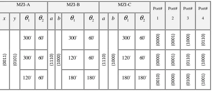
2.3. Boolean Optical Logic Gates using a Single Mach-Zehnder Interferometer ... 29
2.3.1. Theoretical model and 16-logic operation cases ... 30
2.3.2 Simulation results for each logic gate... 35
2.3.3 Complex circuit using the MZI based logic unit ... 40
2.4 Conclusions ... 42
3. All-optical flip-flops ... 45
3.1 State-of-Art of All-Optical Flip-Flops ... 47
3.1.1 Asynchronous AOFF schemes ... 47
3.1.2 Synchronous AOFF schemes... 54
3.1.3 Applications of AOFF in all-optical signal processing ... 58
3.1.3.1 All-optical binary counter ... 58
3.1.3.2 All-optical shift register ... 60
3.1.3.3 All-optical random access memory ... 61
3.1.3.4 All-optical square-wave clock generation ... 62
3.2 Experimental and theoretical demonstration of all-optical flip-flops ... 67
3.2.1 All-Optical S-R Flip-Flops Techniques ... 67
3.2.1.1 All-optical clocked S-R flip-flop based on two coupled SOA-MZI ... 67
3.2.1.2 All-optical S-R flip-flop based on two gain-clamped Reflective Semiconductor Optical Amplifiers (RSOAs) ... 71
3.2.2 All-Optical clocked D Flip-Flops Techniques ... 74
3.2.2.1 All-optical clocked D flip-flop based on coupled SOA-MZI ... 74
3.2.2.2 All-optical clocked D flip-flop using a single SOA assisted symmetric MZI ... 77
3.3 Conclusions ... 91
4. All-optical packet routing ... 93
4.1. All-optical packet switching ... 93
4.1.1 State-of-the-art ... 94
4.1.2 Experimental multi-wavelength optical switching ... 96
4.2. All-optical contention resolution ... 98
4.2.1 State-of-the-art ... 98
4.2.2 Experimental analysis of an all-optical packet routing ... 100
4.3. Conclusions ... 105
5. Conclusions and future work ... 107
5.1 Conclusions ... 107
5.2 Directions for Future Work ... 109
iii
List of acronyms
AOFF All-Optical Flip-Flop
BER Bit Error Rate
BPF Band Pass Filter
CLK Clock
CW Continuous Wave
EDFA Erbium Doped Fiber Amplifier
O/E/O Optical-Electrical-Optical
ER Extinction Ratio
FWM Four-Wave Mixing
HNLF Highly Non-Linear Fiber
MZI Mach-Zehnder interferometer
SOA-MZI Mach-Zehnder Interferometer with Semiconductor Optical
Amplifiers
MZM Mach-Zehnder Modulator
NOLM Non-Linear Optical Loop Mirror
NRZ Non-Return-to-Zero
OCDMA Optical Code Division Multiple Access
PC Polarization Controller
PRBS Pseudo-Random Bit Sequence
PS Phase Shifter
RSOA Reflective Semiconductor Optical Amplifier
RZ Return-to-Zero
SOA Semiconductor Optical Amplifier
WDM Wavelength Division Multiplexing
XGM Cross Gain Modulation
v
List of figures
Figure 1- Schematic of an all-optical router ... 3 Figure 2 - Schematic of an all-optical SOA-MZI switch. ... 12 Figure 3 - Experimental setup to balance the SOA-MZI. ... 14 Figure 4 – (a) SOA-MZI interference at the output ports with PCW= -8dBm. ( b) SOA-MZI
interference at the output ports with PCW= 8dBm. ... 15 Figure 5 - Schematic diagram of the proposed all-optical circuit based on a single SOA-MZI. BPF: Band pass filter, PS: Phase shifter, SOA: Semiconductor optical amplifier. The input ports of the SOA-MZI are #a, #b, #c and the output ports are #I, #J. ... 16 Figure 6 - #I and #J output power as function of (a) SOA1, SOA2 current variation and (b) #a, #c input power. ... 19 Figure 7 - Comparison between measured and modeled output power levels versus #a, #b, #c input logic levels (level 0 0 mW; level 1 0.5 mW). ... 22
Figure 8 - Experimental setups: a) to obtain I =X⋅Y and
J
=
X
⋅
Y
; b) to obtain I = X andX
J
=
; c) to obtain I =Y andJ
=
Y
. ... 23 Figure 9 - Experimentaltime domain traces obtained for Boolean functions I = X⋅Y andY
X
J
=
⋅
. ... 24 Figure 10 - Experimentaltime domain traces obtained for Boolean functions: on the left I = Xand
J
=
X
; on the right I =Y andJ
=
Y
... 25 Figure 11 - Experimental setup a) co-propagation scheme b) counter-propagation scheme. DFB: distributed-feedback laser; PC: polarization controller; MZM: Mach-Zehnder modulator; EDFA: erbium doped fiber amplifier; ODL: optical delay line; VOA: variable optical attenuator; CW: continuous wave; SOA: semiconductor optical amplifier; PS: phase shifter. ... 26 Figure 12 - a) and b) Data sequences c) XOR output.Vertical scale is arbitrary and horizontal scale is 500 ps/div. ... 27 Figure 13 - Performance of all-optical XOR gate Vs Input data signal. ... 28 Figure 14 - Schematic diagram of proposed MZI based 16-logical operation circuit. PM: phase modulator. ... 29 Figure 15 – (a) Variation of normalized output power (a.u.) with ∆θ (in degree). (b) Variation of crosstalk (in dB) with ∆θ (in degree). ... 33 Figure 16 - Proposed configuration of the optical 16-Boolean logic circuit based on a single MZI. ... 35Figure 17 - Simulated curves for each logic gate. a)XY( AND); b) X +Y(NAND); c)XY ; d)
Y
X + ; e)XY; f)X +Y ; g)X⊕Y( XOR); h) X⊕Y(XNOR); i)0 False ; j) ( ) 1 True ; k)( ) X ; l)X ;
m) Y; n)Y ; o)X +Y(OR); p)XY(NOR). ... 36 Figure 18 - Schematic diagram of the optical thresholder circuit. ... 37
Figure 19 - Simulated curves for each logic gate after thresholder function. a)XY( AND); b) )
(NAND Y
X+ ; c)XY ; d)X +Y; e)XY; f)X +Y ; g)X⊕Y( XOR);h)X⊕Y(XNOR); i)0 False ; ( )
j)1 True ; k)( ) X; l)X ; m)Y; n)Y ; o)X +Y(OR); p)XY(NOR)... 38
Figure 20 – (a) Block diagram of our proposed MZI based logic unit. (b) Complex logic circuit using three cascaded MZI. ... 40
Figure 21 - Simulatated waveform of the proposed complex circuit shown in Figure 8(b). ... 42
Figure 22- IEEE Xplore annual citations with index terms referring to optical flip-flops. The lines are visual guides. ... 45
Figure 23 - All-optical S-R flip-flop based on a single SOA-MZI ... 47
Figure 24 - Architecture for the S-R optical flip-flop using a single SOA-MZI and multiple forward signals ... 48
Figure 25 - All-optical S-R flip-flop based on two coupled SOA-MZI. ... 49
Figure 26 - a) Mask layout for two-state multiwavelength laser. b) Operation of device showing laser A suppressing lasing in laser B. SOA: semiconductor optical amplifier; AWG: arrayed waveguide grating . ... 49
Figure 27 - All-optical S-R flip-flop based on SOA fiber ring lasers. ... 50
Figure 28 - All-optical S-R flip-flop based on SOA fiber ring lasers sharing a SOA . ... 51
Figure 29 - All-optical S-R flip-flop based on the bistability of injection locked Fabry-Perot laser diode ... 51
Figure 30 - Schematic diagram of an optical flip-flop based a DFB laser ... 52
Figure 31 - Scheme of an optical S-Rflip-flop based on single micro-ring laser ... 53
Figure 32 - Schematic diagram of optical flip-flop memory on a silicon chip ... 53
Figure 33 - Scheme of the optical clocked S-R flip-flop based on two coupled SOA ring lasers. .. 55
Figure 34 - Scheme of the optical clocked D flip-flop based on two coupled SOA ring lasers. ... 55
Figure 35 - Logic circuits for all-optical clocked T flip-flop ... 56
Figure 36 - Physical model of the all-optical clocked D flip-flop using a single TOAD. ... 57
Figure 37 - Logic circuit for the all-optical clocked S-R flip-flop based on MZI-BLD. ... 58
Figure 38 - Logic circuits for all-optical binary counter ... 59
Figure 39 - All-optical two-bit binary counting at 120 kHz. ... 59
Figure 40 - Optical shift register scheme ... 60
Figure 41 - Results for shifting of the binary sequence 01010011. (a): The 20 kHz clock signal. (b) The output of the optical converter. (c) The output of optical flip-flop 1. (d) The output of optical flip-flop 2. All the signals in panels (b), (c) and (d) are filtered by a filter with a center wavelength of λ2. ... 61
Figure 42 - (a) Layout of the optical static RAM cell. (b) Read mode experimental setup. (c) Write mode experimental setup ... 62
Figure 43 - BER measurements at 5Gb/s for read and write mode operation. ... 62 Figure 44 - All optical square-wave clock generation. Inset figure show the hysteresis loop of the
vii Figure 45 - Optical square-wave clock generation. Insets show the details of the square-wave
regions over 1µs windows of the optical clock ... 63
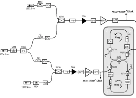
Figure 46 - Experimental scheme of the optical clocked S-R flip-flop. DFB: distributed-feedback laser; PC: polarization controller; MZM: Mach-Zehnder modulator; EDFA: Erbium Doped Fiber Amplifier; ODL: optical delay line; CW: continuous wave laser; BPF: band pass filter; VOA: variable optical attenuator; SOA: semiconductor optical amplifier; PS: phase shifter; PG: pattern generator. ... 68
Figure 47 - Experimental optical asynchronous S-R latch scheme based on two coupled SOA-MZI. ... 68
Figure 48 - Experimental results for asynchronous S-R latch: a) Set signal; b) Reset signal; c) S-R Latch output. The vertical scale is arbitrary and the horizontal scale is 5ns/div. ... 69
Figure 49 - Experimental results: a) clock signal; b) reset signal; c) AND2 optical gate (Set∩Clock); d) AND1 optical gate (Reset∩Clock); e) optical clocked S-R Flip-Flop output The vertical scale is arbitrary and the horizontal scale is 5ns/div for a) b) figures and 10 ns/div for c)d)e). ... 70
Figure 50 - Simulation setup of the all-optical S-R flip-flop based on two coupled lasers. ... 71
Figure 51 - Simulation output results of the AOFF, at the bit rate of 250 Mbit/s. ... 73
Figure 52- Simulation output results of the AOFF at the bit rate of 1Gbit/s. ... 73
Figure 53 - Experimental scheme of the optical clocked D flip-flop based on two coupled SOA-MZI. ... 75
Figure 54 - Optical clocked D flip-flop operation. The vertical scale is arbitrary and the horizontal scale is 5ns/div. ... 76
Figure 55 - Schematic representation of the all-optical D flip-flop based on a single SOA-MZI. D: incoming signal; CLK: clock signal; Q: flip-flop output; ODL: optical delay line; ATT: optical attenuator; BPF: band pass filter. The input ports of the MZI are A, B. ... 77
Figure 56 - Power distribution, along the interferometer arms, for different cases. (a) Case-I: D = 1, CLK = 1, Qn = 0, (b) Case-II: D = 1, CLK = 1, Qn = 1, (c) Case-III: D = 1, CLK = 0, Qn = 1, (d) Case-IV: D = 0, CLK = 0, Qn = 1, (e) Case-V: D = 0, CLK = 1, Qn = 1, (f) Case-VI: D = 0, CLK = 1, Qn = 0, (g) Case-VII: D = 0, CLK = 0, Qn = 0, (h) Case-VIII: D = 1, CLK = 0, Qn = 0. ... 86
Figure 57 - Simulated output of SOA-MZI based all-optical clocked D flip-flop. ... 88
Figure 58 - Output waveforms for different loop length delay time. (a) = 5 ps, (b) = 20 ps, (c) = 40 ps and (d) = 100 ps. ... 90
Figure 59 - Packet forwarding gate based on flip-flop ... 94
Figure 60 - Basic configuration of wavelength routing subsystem ... 95
Figure 61 - 80 Gb/s data packets and the associated eye-diagrams. a) Input; b) and c) switch ports. The eye-diagrams are measured by a 700 GHz optical sampling scope. ... 96
Figure 62 - Experimental setup of a multi-wavelength optical switching node. ... 97
Figure 63 - Experimental results of a multi-wavelength optical switching node.a) at port #J of the switch, b) at port #I of the switch. ... 98
Figure 64 - Contention resolution concept ... 99 Figure 65 - 17 a) BER curves of i) input packets, ii) output of OBF_1, iii) output of SOA-OBF_2. b) 40 Gb/s eye diagrams of i) input packets, ii) inverted signal at SOA-OBF_1, iii)
non-inverted signal at SOA-OBF_1, iv) output of SOA-MZI WC, v) non-inverted signal at 1554 WC, vi) O/P2, vii) O/P1 ... 99 Figure 66 - Block diagram of the contention resolution circuit with priority control ... 100 Figure 67 - Experimental results. (a) Packet stream A, (b) packet stream B, (c) flip-flop (d) MZI_1 (switch 1) switched port, (e) MZI_1 (switch 1) unswitched port, (f) PED, (g) SOA-MZI_2 (switch 2) switched port, (h) SOA-SOA-MZI_2 (switch 2) unswitched port, (j) low-priority contending packets (point 5 of the circuit shown in Fig.66), (k) O/P2, (i) SOA-filter output
(inverting WC) and (l) DI output (O/P1). Time scale: 38 ns/div. ... 100 Figure 68 - Experimental setup of the all-optical packet routing.DFB: distributed-feedback laser; PC: polarization controller; MZM: Mach-Zehnder modulator; EDFA: Erbium Doped Fiber
Amplifier; ODL: optical delay line; VOA: variable optical attenuator; SOA: semiconductor optical amplifier; PS: phase shifter; PG: pattern generator. ... 101 Figure 69 – a) Experimental results of the optical flip-flop based on coupled SOA-MZI. Vertical scale is arbitrary and horizontal scale is 10ns/div. Upper: Set signal; Down: Optical S-R flip-flop output. b) Optical data packets with a 211-1 return-to-zero (RZ) pseudorandom bit sequence
(PRBS). Upper: characteristic of data sequence; Down: eye diagram of data sequence. ... 102 Figure 70 – Packet traffic in a routing system... 104 Figure 71 - BER measurements as function of received power measured at output port #1 (Out 1). Insets: Eye-diagrams measured at Out1 for each analyzed case. ... 105
ix
List of tables
Table 1: Truth table of the proposed all-optical circuit. #a, #b, #c: interferometric input ports; #I, #J: interferometric output ports. ... 17 Table 2: Possible input combinations. ... 20 Table 3: Parameters extracted from the model fittings and used in the final validation. .... 21 Table 4: Parameters used in simulation for the SOA-MZI XOR gate. ... 28 Table 5: Optical AND/NAND logic gate ... 33 Table 6: 16-Boolean optical gates using a single MZI ... 34 Table 7: Extinction Ratio before and after the thresholder circuit. ... 39 Table 8: Inputs and outputs for all ports of complex circuit of Figure 20(b). ... 41 Table 9: Comparison between different all-optical flip-flops techniques. A: asynchronous; S: synchronous; DM: dynamic measurement; SM: static measurement CR: Contrast ratio. ... 65 Table 10: RSOA and simulation parameters ... 72 Table 11: Truth table of the optical clocked D flip-flop... 74 Table 12: Parameters used in simulation. ... 87 Table 13: Truth table of the optical switch ... 97
Chapter 1
Introduction
The exponential growth of internet traffic and new internet-based services (such as video on demand, voice over IP, video teleconference and multimedia services) have been the major driving forces for the increasing demand of transmission bandwidth over the last years. This is making network operators looking for optical approaches in order to allow higher transmission rates, maintaining the efficiency of the network.
All-optical devices can provide data format transparency, higher-speed processing, smaller foot-print and, expectably, lower power consumptions, compared to their electronic counterparts [1]. The optical-electrical-optical (O/E/O) conversions required for routing information between electronic circuits and the optical transmission medium impose a severe bottleneck, which limits the data bit rate and the traffic capacity that can be processed [2]. Today, the current maximum bandwidth obtained by electronic processing is typically around 40 Gb/s, while the maximum capacity of optical transport within a fiber has exceeded 20 Tb/s, which shows the limited speed of electronic processing [3]. An increase in the optical packet bit rate will increase the difficulty in using electronic devices. Indeed, routing a high number of packets per second through the several layers of electronics in a router, can cause router congestion and exceed the performance of electronics and the ability to efficiently handle with the high level of heat generated [4]. Therefore, is desirable that switching and routing can be carried out directly over the optical domain. Such optical packet switch networks require the implementation of digital functions in the physical layer, namely all-optical logic gates and all-optical flip-flops.
All-optical logic gates are crucial devices in optical networks because they can execute essential signal processing functions such as switching, regeneration and header recognition processing in photonic switching nodes. All-optical gates are capable to perform Boolean logic operations at high data bit rate and, in recent years, considerable research has been done mainly due to technology advances in monolithic and hybrid integration. In [5] and [6], a NOT logic gate is demonstrated
1. Introduction
based on a semiconductor optical amplifier assisted Sagnac interferometer and by using a single optical directional coupler configuration, respectively. In [7], an optical NOT gate with variable threshold is implemented using dual wavelength injection locking. In [8], is proposed an all-optical XOR gate with optical feedback using highly Ge-doped nonlinear fiber and a terahertz optical asymmetric demultiplexer, whereas in [9] an optical logic AND gate is implemented based on a nonlinear optical loop mirror (NOLM). Others approaches use an electroabsorption modulator (EAM) [10] or exploit the nonlinearity of semiconductor optical amplifiers such as cross gain modulation (XGM) of SOA based devices [11] and [12] or are based on four-wave mixing phenomenon [13].
A basic building block of any router, electrical or optical, is the memory circuit. It is essential for storing, temporarily, the header information of a packet and for solving the contention problem that occurs when several packets arrive for the same port, at the same time. Using fiber delay lines (FDLs), as an optical buffer to store optical packets, it is possible to prevent packet loss in a switch. When packets arrive at the same time, they are routed to different FDLs, with delay equivalent to the packet length, and the collision can be avoided. However, this technology doesn´t allow neither long-term storage nor random access at an arbitrary timing. Another problem is that FDLs introduce losses that increase with its size [14].
One of the most important optical devices for buffering decisions in next generation photonic transmission systems is the optical flip-flop. This device has at least two stable states and its operation principle is based on hysteresis phenomena, in which is possible to obtain multiple states under the same input conditions. In general, hysteresis can be achieved by a combination of a feedback mechanism and a nonlinear effect. In a conventional flip-flop, the bistability operation is performed in the ‘S-shaped’ hysteretic region, and the output state is distinguished by the different output power while in the optical memory, the state can be distinguished by different output wavelengths [15]. An optical bistable is a sequential device therefore its outputs not only depend of the input values in a considered instant, but also depend of information from a previous state, so it can be used as a one-bit optical memory.
Different technologies have been proposed to implement all-optical flip-flops such as the use of SOA based Mach-Zehnder interferometer (SOA-MZI) with a feedback loop [16], two coupled fiber ring lasers [17] or two coupled SOA-MZI [18]. Among these approaches, the ones that use active interferometric devices have attracted increasing attention because they require low energy to operate, have high compactness and extinction ratio (ER), as well the potential for further optical integration. Exploiting the non-linear effects of active Mach-Zehnder interferometer has enabled the demonstration of most of the novel techniques proposed in this PhD work.
All-Optical Routing Functionalities
3 Clocked flips-flops are some of the most used elements in digital very-large-scale integration (VLSI) systems, but scaling CMOS sequential logic is extremely difficult, namely due to the power consumed of their leakage currents. Therefore, it is so important to find high-speed and low-power optical clocked flip-flops capable to overcome the limitations of CMOS technology. In the last years, most of the research of optical flip-flops has been done considering mainly the asynchronous operation, where any change of information in the flip-flop inputs is transmitted, immediately, to the output according to the truth table. However, in some cases the inputs can suffer unwanted variations and if we are using asynchronous devices, we can be storing unwanted information. The dynamic operation of an asynchronous bistable device can be changed by providing an additional synchronization input (CLK), in order to control the enable of the flip-flop, making it sensitive or not to the values present at its inputs. Most of our work regarding flip-flops is concentrated on devices operating synchronously.
Besides all the known applications that an optical bistable device can fulfill namely, as clock dividers, optical counters and shift registers, optical flip-flops are essential building blocks for implementing all-optical packet routing configurations such as the one shown in Figure 1.
Figure 1- Schematic of an all-optical router.
Figure 1 comprises four main building blocks: the all-optical header/label processing block, the optical buffer unit, the switching stage based on SOA-MZI switches and the collision detection/solver block.
The first functional block performs header processing recognition in the optical domain through autocorrelation. Here, optical code division multiple access (OCDMA) codes are used to encode the packet addresses and sent in a separate wavelength band (out of band signalling). Employing the OCDMA labelling scheme, the routing information is encoded by scrambling the label with a
1. Introduction
specific OCDM code, which may be viewed as a local address [19]. The address recognition unit consists in a well-matched decoder with time reversed impulse response compared to the encoded signal. The fact that optical code processing can be realized in the optical domain provides the possibility to overcome speed limitations due to optical/electrical conversions required in header processing and enhance the energy efficiency of the routing nodes. The proper autocorrelation function of the matching pair is pursued, in order to provide the triggering signal for buffering elements of the routing node. Concerning the management of the spectral addressing band, the encoding process allocates a distinct spectral band compared to the band devoted to data transmission. The second block consists of all-optical flip-flops for holding temporary the packet duration. The third building block of the all-optical packet router consists of two parallel SOA-MZI structures (first SOA-MZI stage of Figure 1) and based on the information coming from the flip-flop output, it switches the optical packets through cross phase modulation (XPM), which results in an interference process, that can be constructive or destructive. Finally, the collision detector and solver blocks are implemented based also on hybrid integrated SOA-MZIs. If both optical packets are routed to the same output port, at the same time, collision is detected by the second SOA-MZI stage of Figure 1 (SOA-MZI3 and SOA-MZI4) and then avoided by the collision solver block based on wavelength conversion.
Others photonic routing schemes have been also designed and experimentally validated. In [20], is proposed a photonic routing system that performs on-the-fly contention resolution between 40 Gb/s packets of the same wavelength whereas in [21] asynchronous packets are routed by combining packet detection, space switching and self-resetting latches.
1.1 Thesis motivation and outline
As described in the previous section, with the continuously growth of Internet traffic, it is necessary to develop new techniques and devices capable to support the huge bandwidth required by the future services, with scalability and flexibility. This scenario stimulates us to research and develop innovative high-speed photonics solutions, such as all-flip-flops and logic gates, for the effective operation of transparent optical networks. Some of the research results presented in this work were performed under the EU NoE EURO-FOS project consortium and it was performed mainly in the facilities of Instituto de Telecomunicações (IT) in Aveiro, and during a one-week stay at the photonic lab of the National Technical University of Athens, in Greece. The following
All-Optical Routing Functionalities
5 chapters present an analysis and novel concepts of some of the main building blocks of all-optical packet routing schemes. This thesis is constituted by five chapters, organized as follows.
Chapter 1 provides a brief background about photonic transmission systems and devices, and describes the organization of the thesis as well as its main scientific contributions to the state-of-art.
Chapter 2 focuses on the design and operation principle behind all-optical logic gates, since they are a fundamental element for the development of complex processing functionalities. Two novel optical logic gates configurations, capable to perform different logic operations, are presented and described. The first method is experimentally and numerically demonstrated and uses, simultaneously, both output ports of an active interferometer. The second configuration is based on a single Mach-Zehnder interferometer, with controlled phase modulators, and performs different Boolean logic operations without changing setup design. The non-linear behavior of a SOA-MZI is also described regarding gain and phase dynamics, since it is the base of most of the applications studied and proposed throughout this PhD work. An all-optical logic XOR gate based on a SOA-MZI, is also compared in terms of the way the incoming signal is injected (co or counter propagation) via numerical simulations and experimentally.
Chapter 3 presents an overview of the state of the art on all-optical flip-flops, discussing their basic designs and theoretical concepts. We appraised, quantitatively, in terms of commuting speed, switching energy and integration capability some of the most relevant experimental AOFF implementations and the obtained results demonstrate the suitability of them in next generation communication systems. In this chapter, we also proposed four new all-optical flip-flop configurations, experimentally and by means of simulation, focusing mainly in bistables whose state switching is triggered by a pulsed clock signal.
Chapter 4 addresses the technical solution of the contention problem that can arise from packets aiming the same switch port but, firstly, an overview of some of the most preeminent all-optical routing designs, with particular relevance for the ones using SOA-MZI structures, is outlined. The reminiscent power of the blocked packets, due to the non ideal switching performed by the SOA-MZIs, is analyzed in every stage of the routing configuration and the performance transmission is experimentally evaluated through BER measurements and extinction ratio analysis.
Chapter 5 overviews the developed work, summarizes the main conclusions, and presents suggestions for future work.
1. Introduction
1.2 Main contributions
The main contributions of this work can be summarized as follows:
Development and experimental demonstration of four optical Boolean operations based on a single SOA-MZI, using simultaneously both output ports.
Investigation of an all-optical logic XOR gate and assessment of its performance in co and counter propagation schemes.
Development and validation through numerical simulation of an optical configuration that provides 16 optical logic operations, using a single MZI with controlled phase modulators in each arm, without changing the setup scheme.
Proposal and experimental implementation of all-optical S-R and D type clocked flip-flops, using SOA-MZI structures.
Proposal and performance demonstration, through numerical simulations, of an all-optical S-R flip-flop using two gain-clamped S-RSOAs.
Proposal and theoretical analysis of an all-optical clocked D flip-flop using a single SOA assisted symmetric MZI.
Identification and experimental demonstration how the reminiscent power of blocked packets from non ideal SOA-MZIs can affect the data performance transmission.
1.3 List of publications
The work accomplished during the elaboration of this PhD work resulted in 13 papers published/ submitted in internationally peer reviewed journals and 16 international conference proceedings. The publications are listed below.
1.3.1 Journal Articles
[J1] C. Reis, T. Chattopadhyay, P.S. André, A. Teixeira, "Single Mach-Zehnder interferometer based Boolean logic gates", Applied Optics, Vol. 51, no. 36, pp. 8693 - 8701, December
All-Optical Routing Functionalities
7 [J2] C. Reis, T. Chattopadhyay, G. Parca, R. Dionísio, P. André, A. Teixeira, " All-optical multifunctional logic operations using simultaneously both interferometric output ports in a symmetric SOA-MZI”, submitted to Optics and Laser Technology.
[J3] C. Reis, L. Costa, A. Bogoni, A. Maziotis, A. Teixeira, C. Kouloumentas, D. Apostolopoulos, D. Erasme, G. Berrettini, G. Meloni, G. Parca, H. Brahmi, I. Tomkos, L. Poti, M. Bougioukos, P. S.André, P. Zakynthinos, R. Dionisio, T. Chattopadhyay, H. Avramoupoulos, "Evolution of all-optical flip-flops and their applications", IET
Optoelectronics, Vol. 6, no. 6, pp. 263 - 276, December 2012.
[J4] C. Reis, A. Maziotis, C. Kouloumentas, C. Stamatiadis, N. Calabretta, P.S. André, R.P. Dionísio, B. Neto, H.J.S Dorren, H.Avromopoulos, A.T. Teixeira, "All-optical synchronous S-R flip-flop based on active interferometric devices", Electronics Letters, Vol. 46, no. 10, pp. 709 - 710, May 2010.
[J5] C. Reis, A. Maziotis, C. Kouloumentas, C. Stamatiadis, N. Calabretta, P.S. André, R.P. Dionísio, B. Neto, H.J.S Dorren, H.Avromopoulos, A.T. Teixeira, "All-Optical Clocked D Flip-Flop Memory using a Hybrid Integrated S-R Latch”, Microwave Optical Technology
Letters, Vol. 53, no.6, pp.1201-1204, June 2011.
[J6] R. Dionísio, G.P. Parca, C. Reis, A. T. Teixeira, "Operational parameter optimization of MZI-SOA using multi-objective genetic algorithms", Electronics Letters, Vol. 47, no.9, pp.561-56, April 2011.
[J7] C. Reis, A. Maziotis, C. Kouloumentas, T. Chattopadhyay, N. Calabretta, P.S. André, G. Berretini, G. Meloni, H.J.S Dorren, A. Teixeira, "Performance comparison of all-optical clocked S-R and D type flip-flops", Optik - Intrnl. Journal for Light and Electron Optics, Vol. 1, no. 1, pp. 1 - 7, December 2012.
[J8] T. Chattopadhyay, C. Reis, P.S. André, A. Teixeira, "Theoretical analysis of all-optical clocked D flip-flop using a single SOA assisted symmetric MZI", Optics Communications, Vol. 285, no. -, pp. 2266 - 2275, April 2012.
[J9] C. Reis, G. Parca, M. Bougioukos, A. Maziotis, S.Pinna, H. Brahmi,G. Giannoulis P.André, N. Calabretta, V. Vercesi, G. Berrettini, C. Kouloumentas, A. Bogoni, T. Chattopadhyay, D. Erasme, H. Avramoupoulos, A. Teixeira, “Experimental analysis of an all-optical packet routing”, IEEE/OSA Journal of Optical Communications and Networking, Vol. 6, No. 7, pp. 629–634, July 2014.
[J10] B. Neto, C. Reis, R.P. Dionísio, J. Ferreira, J. Lázaro, G. Tosi-Beleffi, A.N. Pinto, R. N. Nogueira, A.T. Teixeira, P.S. André, "Assessment and mitigation of EDFA gain transients in hybrid WDM/TDM PON in the presence of packet based traffic", IET Optoelectronics,
SPECIAL ISSUE ON Next Generation Optical Access, Vol. 4, No. 6, pp. 219 - 225,
December 2010.
[J11] B. Neto, A. K. Klingler, C. Reis, R.P. Dionísio, R.N. Nogueira, A.T.Teixeira, P.S André, “Enhanced optical gain clamping for upstream packet based traffic on hybrid WDM/TDM-PON using fiber Bragg grating", Optics Communications, Vol. 284, No. 5, pp. 1354 - 1356, March 2011.
1. Introduction
[J12] R.P. Dionísio, G. Parca, C. Reis, R.N. Nogueira, A. Teixeira, "2x10Gbit/s NRZ-OOK to 10Gbaud Quasi Continuous Phase Modulation All-Optical Conversion Using Cascaded MZI- SOAs", Microwave and Optical Tech. Letters, Vol. 54, No. 5, pp. 1240 - 1242, March 2012.
[J13] J. Girão, B. Neto, A.M.Rocha, C. Reis, R.P. Dionísio, S. Chatzi, F Bonada, J. Lazaro, A. Teixeira, P.S André, "C+L band extended reach amplified next generation access networks", Microwave and Optical Tech. Letters, Vol. 53, No. 10, pp. 2414 - 2418, October 2011.
1.3.2 International Conferences
[C1] C. Reis, R.P. Dionísio, B. Neto, A.T. Teixeira, P.S. André, "All-Optical XOR Based on Integrated MZI-SOA with Co and Counter-Propagation Scheme", in Proceedings of IEEE
International Conf. on Transparent Networks – Mediterranean Winter - ICTON MW,
Angers, France, pp. FrP.11, December 2009.
[C2] G. Parca, R. Dionísio, C. Reis, S. Betti, G. Tosi Beleffi, A. Teixeira, “Inherent fabrication yields and asymmetries impacts on MZI-SOA static modeling”, in Proceedings of IEEE International Conf. on Transparent Networks – ICTON, Munique, Germany, pp. Mo.P.22, June 2010.
[C3] C. Reis, R.P. Dionísio, B. Neto, P.S. André, A. Teixeira, "All-Optical Phase Modulation using MZI-SOA", in Proceedings of European Conf. on Networks and Optical Communications and Conf. on Optical Cabling and Infrastructure - NOC/OC, Faro, Portugal, June 2010.
[C4] R.P. Dionísio, C. Reis, P.S. André, R. Nogueira, A. Teixeira, “Experimental Study of a Phase Modulator Using an Active Interferometric Device”, in Proceedings of IEEE Mediterranean Electrotechnical Conference – MELECON, La Valletta, Malta, pp. 1142 – 1146, April 2010.
[C5] C. Reis, A. Maziotis, C. Kouloumentas, C. Stamatiadis, N. Calabretta, P.S. André, R.P. Dionísio, B. Neto, H.J.S Dorren, H.Avromopoulos, A.Teixeira, “Experimental Evaluation of All-Optical Asynchronous and Synchronous Memories”, in Proceedings of IEEE 6th Computer Engineering Conference –ICENCO, Cairo, Egypt, December 2010.
[C6] V.M.C. Ribeiro, C. Reis, M.J.N. Lima, P.S. André, A.T. Teixeira; “All-Optical Flip Flop Using Two Gain-Clamped RSOAs”, in Proceedings of IEEE International EUROCON and CONFTELE 2011, Lisbon, Portugal, April 2011.
[C7] T.Chattopadhyay, C.Reis, P.André and A.Teixeira, “All-Optical Clocked D Flip-Flop using a single SOA-MZI”, in Proceedings of IEEE 13th International Conference on Transparent Optical Networks, ICTON 2011, Tu.B1.6, ,Stockholm, Sweden, June 2011.
[C8] C. Reis, B. Neto, R.P. Dionísio, G. I. Incerti, G. Tosi-Beleffi, D. Forin, A.M. Rocha, A.T. Teixeira, P.S. André, "Transience analysis of bursty traffic with Erbium Doped Fiber Amplifiers", in Proceedings of IEEE International Conf. on Transparent Networks – ICTON, Açores, Portugal, pp. Tu.B2.4, June 2009.
All-Optical Routing Functionalities
9 [C9] B.Neto, C. Reis, A.M. Rocha, A.T. Teixeira, N. Wada; P.S. André, "Transience response of traffic based on optical packets with optical amplifiers", in Proceedings of European Conf. on Networks and Optical Communications - NOC, Valladolid, Spain, pp. 545 - 550, June 2009.
[C10] P.S. André, B. Neto, C. Reis, A.M. Rocha, N. Wada, G. Beleffi, A.T. Teixeira, "Raman amplification challenges for next generation networks", in Proceedings of IEEE International Conf. on Transparent Networks – ICTON, Açores, Portugal, pp. Tu.A2.2, June 2009.
[C11] B. Neto, C. Reis, A.T. Teixeira, P.S. André, N. Wada, "Gain equalization technique for Raman amplification systems based on the hybrid optimization algorithm", in Proceedings of IEEE International Microwave and Optoelectronics Conference - IMOC, Belém do Pará, Brasil, pp. 687 - 689, November 2009.
[C12] B. Neto, A. K Klingler, C. Reis, J. P. G. Girão, A.T. Teixeira, P.S. André, "EDFA Transient Assessment for Bursty Traffic", in Proceedings of IEEE International Conf. on Transparent Networks – Mediterranean Winter - ICTON MW, Angers, France, pp. FrP.6, December 2009.
[C13] R. P. Dionisio, C. Reis, N. Pavlovic, R.Nogueira, A. Teixeira, “Dual MZI-SOA with Serial Configuration for Quadrature Phase Modulation”, in Proceedings of European Conf. on Networks and Optical Communications and Conf. on Optical Cabling and Infrastructure - NOC/OC, Faro, Portugal, pp. 307 - 309, June 2010.
[C14] B. Neto, A.M. Rocha, J.P. Girão, R.P. Dionísio, C. Reis, A. Teixeira, P.S. André, J. Lazaro, “Comparative analysis of hybrid in line EDFA/Raman with simple Raman amplification in WDM ring PON for C+L band”, in Proceedings of European Conf. on Networks and Optical Communications and Conf. on Optical Cabling and Infrastructure - NOC/OC, Faro, Portugal, June 2010.
[C15] B. Neto, A.M. Rocha, J.P. Girão, R.P. Dionisio, C. Reis, S. Chatzi, F. Bonada, J. Lazaro, A. Teixeira, P.S. André, “C+L band gain equalization for extended reach WDM-ring PON using hybrid Raman/in-line EDFA amplification”, in Proceedings of IEEE International Conf. on Transparent Networks – ICTON, Munich, Germany, pp. We.P.18, June 2010.
[C16] B. Neto, R. P. Dionisio, A. M. Rocha, C. Reis, S. Chatzi, F. Bonada, J. Lazaro, A. Teixeira and P. S. André, "C+L band extended reach next generation access networks through Raman amplification: assessment in rural scenario", in Proceedings of IEEE 15th International Optoelectronics and Communications Conference – OECC, Sapporo, Japão, pp. 22 - 23, July 2010
Chapter 2
Optical logic gates
In the last few years, optical logic gates have been widely investigated in order to overcome the speed limitation of electrical signal processors. All-optical gates can be used in a variety of signal processing applications, such as optical bit pattern recognition, optical time division demultiplexing, optical bit-error rate monitoring, optical label swapping as well as in optical binary adders and optical counter [22, 24].
Several approaches have been proposed up-to-date to demonstrate different optical logic operations and mostly are based on highly nonlinear optical fibers (HNLFs), on microring or on nonlinear effects in semiconductors optical amplifiers (SOAs), integrated or not in interferometric structures. The HNLF-based logic gates exploit the Kerr effect of silica, through a response in few femtosecond range however, despite the significant advances in fabrication technology, HNLFs still present severe limitations when integration is required. In general, optical logic gates based on the nonlinear effects in SOAs, such as cross-gain modulation (XGM), cross-phase modulation (XPM), four wave mixing (FWM) and cross polarization modulation have been preferred mainly due to their high potential for photonic integration and cascadability, high gain of SOAs and strong change of the refractive index. However, they present speed limitation and latency, primarily due to the slowly recovery time of the SOAs. Operation speed can be increased with the integration of SOAs in interferometer structures, especially in Mach-Zehnder interferometers.
Semiconductor optical amplifiers in Mach-Zehnder interferometers (SOA-MZI) are the key devices for the majority of the all-optical processing functionalities studied and proposed in this PhD thesis, therefore a characterization of this device will be made in this work.
This chapter, based on journals [J1], [J2], [J6] and conferences [C1], [C2], [C3], [C4], starts with the presentation of the operation principle of the SOA-MZI and explains the steps to balance the interferometer so it can work properly. In Section 2.2, we propose and experimentally demonstrate a configuration based on a single hybrid integrated SOA-MZI switch capable to carry
2. Optical logic gates
out different logic operations at the same time, using simultaneously both output ports of the interferometer. In this section, we also perform a comparison study of an all-optical logic XOR gate based on a SOA-MZI, implemented in co and counter propagation way. In Section 2.3, we present a novel scheme that performs 16-Boolean logic operations based on a single Mach-Zehnder interferometer with controlled phase modulators, using the same design. The novel configurations proposed in this chapter present very low complexity and suggest high integration potential. Finally, in section 2.4, a summary of the research topics discussed in this chapter is drawn.
2.1 Mach-Zehnder interferometer structures with semiconductor optical
amplifiers (SOA-MZI)
SOA-MZIs are widely used in many optical applications since they perform a variety of optical functions such as, on-off keying (OOK) and multi-format optical signals regeneration, wavelength conversion, all-optical switching, high-speed logical processing and, more recently, optical contention resolution. The SOA-MZI is an element that provides high extinction ratio, high operation speed, requires low switching energies to operate and have high integration capability and compactness.
2.1.1 Operation principle of SOA-MZI
In this PhD work, we propose optical circuits mostly based on the symmetrical hybrid integrated SOA-MZI shown in Figure 2, where each arm incorporates one Semiconductor Optical Amplifier (SOA1 or SOA2) and one Phase Shifter (PS1 or PS2).
All-Optical Routing Functionalities
13 Although it is possible to operate active interferometer structures with discrete components, monolithic or hybrid integration allows longer term stability. K3 and K4 are couplers of the SOA-MZI based switch for dividing and combining the incoming data entering at ports #B or/and #C. The power at the interferometric outputs (#I and #J) is a result of an interference process occurring in coupler K4. The electromagnetic fields at this coupler will define the conditions for the output measurements [26].
The SOA-MZI operation principle is based on cross phase modulation effect and relies on the dependency of the refractive index on the carrier density in the active region of the SOA. A control signal that depletes the carrier density will modulate the refractive index and thereby result in a phase modulation of the incoming data coupled into the SOA-MZI. For example, if one control signal is injected into one of the MZI input ports (#A or #D), through the directional couplers K1 or K2, it will deplete the carriers density of the corresponding SOA. When the SOA is under gain saturation, the refractive index will change as a consequence of the gain saturation variations and a phase difference is created in the signals being amplified. In this case, the incoming data flow out to the respective bar output ports. However, if the control signals are launched simultaneously into ports #A and #D, SOA1 and SOA2 will have the same carrier density, so will not suffer a change in their refractive index and thereby the incoming data will exit from the respective output cross-ports. The same happens when there is no control signals applied into the SOA-MZI switch.
The band pass filters (BPF), placed at the output ports, are used to recover the incoming data and to block the control signals.
2.1.2 Balancing the SOA-MZI
In this subsection, is explained the balancing process that is realized each time an experiment using active interferometers - SOA-MZI – is implemented.
Due to very small changes in motherboard fabrication there is a very small effective path length difference in each arm of the MZI, which causes a small phase change and slightly unbalance the MZI. Similar effects are also seen in the SOAs contained in each arm of the MZI. Therefore, when we are using SOA-MZI structures it is very important to firstly balance the interferometer to get it to work properly. The SOA-MZI is balanced when a maximum extinction ratio (ER) between the interferometer output ports is achieved.
For the balancing process of a SOA-MZI, we use the experimental setup depicted in Figure 3. Firstly, we connect a continuous wave signal (CW) into port #B of the device, followed by a polarization controller (PC), and then set the power to a typical value, for example 1 dBm, with a
2. Optical logic gates
variable optical attenuator (VOA). Since the device is optically symmetric, the CW signal can also be coupled to one of the following SOA-MZI ports: #C, #I or #J. Then, we monitored the output power at port #I and #J with two power meters (PM). Note that is also possible to measure simultaneously the output power at both ports using a single power meter but, in this case, an optical switch connected at ports #I and #J is needed.
Figure 3 - Experimental setup to balance the SOA-MZI.
When the Peltier controller is powered on and the temperature of the device is stabilized (26º C), we set the bias current of both SOAs to an equal value, adjust the input CW polarization and apply a voltage to one or both phase shifters to obtain a minimum power value on the destructive MZI output (port #I) and a maximum power at the constructive port (Port #J). In the end, normally a small detuning on the SOA bias current and in the input power is needed in order to improve the ER, but at every change, we need to re-adjust the voltage of the phase shifters and the input polarization.
In order to obtain the maximum extinction ratio (ER) between the output ports, tunable filters are placed at the MZI output ports to improve the balancing results.
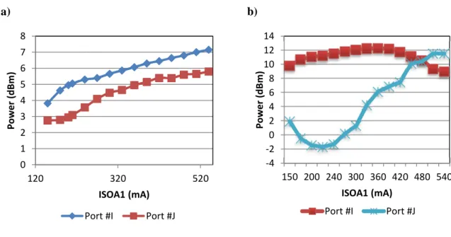
In Figure 4, we vary from 150 mA to 540 mA the bias current of SOA1 (ISOA1), maintaining constant the bias current of SOA2 (ISOA2=200 mA). The mean power of the incoming signal, injected into port #B of the SOA-MZI was increased from -8 dBm (in Figure 4 (a)) to 8 dBm (in Figure 4 (b)). These experimental results highlight the fact that by changing the operational parameters, the interference process suffers considerable changes. We can see clearly that in Figure 4 (b), even without input CW polarization and phase shifters adjustments, a better operational point was achieved. It is also noticeable that in Figure 4 (b), at certain moment, the constructive output port converts in the destructive port, and vice versa, only by changing some system parameters and not by injecting a control signal into SOA-MZI.
All-Optical Routing Functionalities
15 Figure 4 – (a) SOA-MZI interference at the output ports with PCW= -8 dBm. ( b) SOA-MZI interference at the
output ports with PCW= 8 dBm. Lines are visual guides.
2.2 All-optical logic operations using a symmetric SOA-MZI
Logical operation using a single SOA-MZI switch is an attractive technology due to the small device size, low power consumption and complexity. Depending on the signals applied into its input ports, a single SOA-MZI switchis capable to carry out different logic operations at the same time, using simultaneously both output ports of the SOA-MZI. Traditional logic gates have a single output, but if we take advantage of the two output ports of the SOA-MZI based interferometric switch as logical outputs, it is possible to obtain multi output logic functions. Using this concept, we proposed a novel all-optical configuration capable to carry out four logic operations, using simultaneously both output ports of the SOA-MZI. The performance of such architecture is assessed measuring the obtained extinction ratio (ER) for each Boolean function. The proposed circuit is simulated and experimentally demonstrated, using NRZ-OOK modulated signals driven at 10 Gb/s.
2.2.1 Operation principle
Four Boolean operations (AND, Transposed INHIBITION, EQUIVALENCE, INVERTER) can be performed depending of the signals applied into the input ports #a, #b and #c of the
a) b) 0 1 2 3 4 5 6 7 8 120 320 520 P o w e r (d B m ) ISOA1 (mA) Port #I Port #J -4 -2 0 2 4 6 8 10 12 14 150 200 240 300 360 420 480 540 P o w e r (d B m ) ISOA1 (mA) Port #I Port #J
2. Optical logic gates
interferometric structure illustrated in Figure 5. At the output ports #I and #J, optical band pass filters are placed in order to recover the signal injected into port #b.
Figure 5 - Schematic diagram of the proposed all-optical circuit based on a single SOA-MZI. BPF: Band pass filter, PS: Phase shifter, SOA: Semiconductor optical amplifier. The input ports of the SOA-MZI are #a, #b,
#c and the output ports are #I, #J.
Table 1 represents the truth table of the proposed circuit and from this table it is possible to obtain the logical expression at the output ports. Therefore, the Boolean equations at the interferometric output ports, expressed in the disjunctive canonical form, are given by
c
b
a
c
b
a
J
c
b
a
c
b
a
I
⋅
⋅
+
⋅
⋅
=
⋅
⋅
+
⋅
⋅
=
(2.1)Where the symbols ‘⋅’ and ‘ ’ indicate logical ‘AND’ and ‘INVERTER/NOT’ expression, respectively. Equations (2.1) are already in their simplified form, so it is not necessary to use Karnaugh maps or apply Boolean algebra to obtain a simpler solution.
Consider two modulated signals X=[10010000] and Y=[00010010], at the same wavelength, and a continuous signal at a different wavelength. If signals X and Y are injected, respectively, at port #a and port #b of the SOA-MZI switch (no signal at port #c), according to equation (2.1) the logical expressions at the output ports can be written as
(2.2)
Y
X
Y
X
Y
X
J
Y
X
Y
X
Y
X
I
⋅
=
⋅
⋅
+
⋅
⋅
=
⋅
=
⋅
⋅
+
⋅
⋅
=
0
0
0
0
All-Optical Routing Functionalities
17 which correspond to the logic ‘AND’ and ‘Transposed INHIBITION’ operations between the two modulated optical beams. Also, based on this case, an ‘EQUIVALENCE’ and ‘NOT’ logic operations can be obtained, simultaneously, at port #I and port #J of the SOA-MZI if the signal X is launched at port #a and the continuous signal at port #b.
In this situation, the logic equations at the interferometric output ports are
Table 1: Truth table of the proposed all-optical circuit. #a, #b, #c: interferometric input ports; #I, #J: interferometric output ports.
On the other hand, if signal Y is injected at port #c while at port #b we maintain the continuous wave signal, the logical expressions at the output ports #I and #J can be written according to equation (2.1) as
Expected logic levels
Experimental static power measurements (dBm) Inputs Outputs a b c I J I J 0 0 0 0 0 -12,2 -12,2 0 0 1 0 0 -12,1 -13,7 0 1 0 0 1 -10,4 9,1 0 1 1 1 0 7,5 -8,7 1 0 0 0 0 -13,7 -12,2 1 0 1 0 0 -13,7 -12,4 1 1 0 1 0 7,9 -8,2 1 1 1 0 1 -11,2 2,4 X X X J X X X I = ⋅ ⋅ + ⋅ ⋅ = = ⋅ ⋅ + ⋅ ⋅ = 0 1 0 1 0 1 0 1 (2.3)
2. Optical logic gates
(2.4)
From these two latter cases, we can conclude that if a control signal is injected at port #a or port #c of the SOA-MZI, the two even parts of the continuous wave signal (injected at port #b) will propagate through the two MZI arms and will suffer different gains and phase shifts, leading to the unbalance of the SOA-MZI. In these cases, the modulation of the refractive index will not be the same (nSOA1≠ nSOA2) and the light in the upper arm of the MZI will present a different velocity than the lower arm; hence a replica of the control signal appear at port #I (EQUIVALENCE operation), and its complementary at port #J (NOT operation). This technique to implement the NOT operation is designed with a very simple logic circuit since it is performed using only two optical signals (one modulated and another continuous), contrary to the NOT implementations that uses three optical signals. In section 3.2, using also two optical signals, we implemented a NOT gate based on cross gain modulation in a SOA to realize our all-optical D synchronous flip-flop. To perform the XGM based NOT gate, a modulated signal (with λ1) was injected in a SOA and modulated the gain of the amplifier due to its saturation. We coupled to the modulated signal a continuous wave (with λ2), which was modulated by the gain variation of the SOA, and at the output of the SOA, a band pass filter to eliminate the signal with wavelength λ1. The advantage of this technique lies in its simplicity, polarization independence and insensitivity to the wavelength of the modulated data (provided it is within the SOA gain bandwidth). However, presents some disadvantages such as a decreased extinction ratio for up-converted signals and pattern effects of the SOA due to the slow recovery time [27].
2.2.2 Black box static model
Our logic configuration is characterized experimentally in terms of non-ideal splitting factors and SOA1, 2 gains, following the method adopted in [26].
The measurements of SOA-MZI output power as function of input power and SOA current is made considering the two arms separately, using forward propagation, from input #a to output #I, with SOA2 disabled and, similarly, from input #c to output #J, with SOA1 disabled. The trends of the SOA output power vs. SOA current and input power are found and the obtained curves are shown in Figure 6(a) and Figure 6 (b). It is worth noting that this characterization is referred to the
Y Y Y J Y Y Y I = ⋅ ⋅ + ⋅ ⋅ = = ⋅ ⋅ + ⋅ ⋅ = 1 0 1 0 1 0 1 0
All-Optical Routing Functionalities
19 overall path on which the signal propagates, so it takes into account losses and any other kind of asymmetry of the device.
The power at the output of the SOA-MZI (#I and #J) is a result of an interference process occurring in coupler α. The electromagnetic fields at the two inputs of this coupler will define the conditions for the outputs measured. So, specifically, when used as an amplitude modulator, one important factor to take into consideration is the ER of the output signal. For example, through SOAs input power/current variation, the power distribution on the SOA-MZI arms can be further changed, leading to the consequent variation of the interference conditions on output couplers.
a) b)
Figure 6 - #I and #J output power as function of (a) SOA1, SOA2 current variation and (b) #a, #c input power.
Lines are visual guides.
Moreover, a phase shift on SOAs output signals is induced due to the dependence of SOAs refractive index on carrier density.
We model the working characteristic for a SOA-MZI, in order to describe how physical parameters actually control the interference depth, thus providing a tool for operational point optimization, which for example can be used for maximizing ER.
The output powers PI (port #I) and PJ (port #J) are indirectly computed as a function of the SOAs’ total input power level and SOAs’ bias current (Isoa) through SOA 1,2 gain curves reported in Figure 6.
In Table 2, all the 3-bit words obtained combining the 0-1 levels on the inputs #a, #b, #c are considered and identified through the index i=1,…8.
2. Optical logic gates
Table 2: Possible input combinations.
Input i =1 i =2 i =3 i =4 i =5 i =6 i =7 i =8
#a 0 0 1 1 0 0 1 1
#b 1 1 1 1 0 0 0 0
#c 0 1 0 1 0 1 0 1
A black box model, representing the relation between #I and #J output power as function of input power on port #b, obtained from interferometric structure principles considering the couplers yield, path differences and non-ideality, is given by [26]:
Where α is the splitting factor of the last coupler evaluated experimentally. P1bi and P2bi are the
power levels on λb at the input of the rightmost coupler in Figure 5.
∆
φ
i is the phase difference between the two arms, which depends on the individual phase shift induced by the input #a on upper armi
a
φ
∆ , input #c on lower arm
i c φ ∆ and input #b 0 b φ
∆ on both arms. The first two are considered linear with the respective input power, because of the linear relation between SOA induced phase and carrier density, through refractive index variation, taking into account that the
SOAs’ current was kept constant. The last phase shift is considered constant at the value
2
π
due to
the initial balancing operation. The other internal couplers yield, path length differences between the upper and lower arms, the SOA carrier density variations and non-ideality of the tested architecture, are taken into account through further phase delays s1i and s2i.
The SOA-MZI black box static model provides a general frame of how parameters control the interference depth, thus providing a tool for operational point optimization, which for example can be used for maximize the ER.
The parameters’ values of the black box model, α estimated experimentally and the others through MATLAB, are reported in Table 3 and used for the final validation, carried out considering the measured output powers PI and PJ, with Isoa1 and Isoa2 constant at 240 mA.
2 ) sin( ) 1 ( 1 ) sin( 1 ) 1 ( 0 2 2 1 2 1 2 1 2
π
φ
φ
φ
φ
φ
α
α
φ
α
α
+ − = ∆ + ∆ − ∆ = ∆ + ∆ + − + = + ∆ − + − = c a b c a i i b b b i i b b b i kP kP s P P P b P i J P s P P P b P i I P i i i i i i i i i i (2.5)All-Optical Routing Functionalities
21 Table 3: Parameters extracted from the model fittings and used in the final validation.
α ∆
0.51 6,3x10³ rad −1 ÷ 2 rad −1 ÷ 2 rad
After balancing the SOA-MZI, the basic switching operation is performed injecting a signal on port #a or #c: this will produce the interference inversion so that the injected signal will be forwarded through port #I, while the power on port #J is minimized.
In order to verify the logical operations, we use MATLAB environment and the black box model. At the output ports we measured the power levels corresponding to the expected logic operation on the wavelength of the signal injected in #b input, . Thus, in all the cases where port
#b is set to zero, no wavelength conversion was performed.
In Figure 7, we present the comparison among the obtained experimental static power measurements shown in Table 1 and the modeled output power levels. Through the static black box model, it is possible to find a good matching with the correct output levels, applying the optimization of all the parameters that affect the output interference, exactly as it happens experimentally when the maximum ER between the port #I and #J has to be achieved.
The ER optimization is strictly dependent on each inputs combination, due to the different XGM/XPM effect induced by the two SOAs. The 4th case (input combination=111), illustrated in Figure 7, explains how the power levels and the ER are reduced in practice because of the gains saturation and the presence of the three inputs a#, b#, c# set at logical level 1.
The interference depth can be maximized in theory and in practice through adjustments of the phase shifters contribution; in our formulation for the static model we included their contributions in the parameters and .
For all these reasons, the ER maximization in practice is obviously achieved differently for each case. This is why, for example, cases 2 (input combination=011) and 3 (input combination=110) are slightly different in power levels and ER, although the input configuration is the same, except for injecting signal at input #c in case 2 and at input #a in case 3.


![Figure 23 - All-optical S-R flip-flop based on a single SOA-MZI [41].](https://thumb-eu.123doks.com/thumbv2/123dok_br/15747435.1073279/71.892.257.700.622.839/figure-optical-flip-flop-based-single-soa-mzi.webp)
![Figure 24 - Architecture for the S-R optical flip-flop using a single SOA-MZI and multiple forward signals [43]](https://thumb-eu.123doks.com/thumbv2/123dok_br/15747435.1073279/72.892.220.685.361.570/figure-architecture-optical-using-single-multiple-forward-signals.webp)