SLOA093 – December 2001
Filter Design in Thirty Seconds
Bruce Carter High Performance Analog
ABSTRACT
Need a filter—fast? No theory, very little math—just working filter designs, and in a hurry? This is the right document.
Contents
1 Introduction ... 2
2 Low Pass Filter ... 4
3 High Pass Filter ... 5
4 Narrow (Single Frequency) Band Pass Filter... 6
5 Wide Band Pass Filter ... 7
6 Notch (Single Frequency Rejection) Filter ... 8
7 Band Reject Filter ... 9
Appendix A—Standard Resistor and Capacitor Values... 12
Appendix B—Filter Notes (for the More Technically Minded) ... 13
Figures Figure 1. Low Pass Filter... 2
Figure 2. High Pass Filter... 2
Figure 3. Narrow (Single Frequency) Band Pass... 3
Figure 4. Wide Band Pass ... 3
Figure 5. Notch Filter—Single Frequency Rejection ... 3
Figure 6. Band Reject Filter ... 4
Figure 7. Low Pass Filter for ±±±± Supplies ... 4
Figure 8. Low Pass Filter for a Single Supply... 4
Figure 9. High Pass Filter for ±±±± Supplies ... 5
Figure 10. High Pass Filter for a Single Supply... 5
Figure 11. Narrow Band Pass Filter for ±±±± Supplies ... 6
Figure 12. Narrow Band Pass Filter for a Single Supply... 6
Figure 13. Wide Band Pass Filter for ±±±± Supplies ... 7
Figure 14. Wide Band Pass Filter for a Single Supply... 7
Figure 15. Narrow Band Pass Filter for ±±±± Supplies ... 8
Figure 16. Narrow Band Pass Filter for a Single Supply... 9
Figure 17. Band Reject Filter for ±±±± Supplies ... 10
1 Introduction
This document is intended for designers that do not have the time to check filter theory in old college textbooks—and try to translate transfer equations into something that can be put into production. This is like looking at the back of the textbook for the answer. Speaking of the back of the book—Appendix B contains a brief introduction to the filter circuits given here, and the limitations of this quickie approach to design.
To design a filter, four things must be known in advance:
• The power supplies available: positive / negative—or only positive (single supply)
• The frequencies that need to be passed, and those that need to be rejected.
• A transition frequency, the point at which the filter starts to work—or—a center frequency around which the filter is symmetrical.
• An initial capacitor value—pick one somewhere from 100 pF for high frequencies to 0.1 µF for low frequencies. If the resulting resistor values are too large or too small, pick another capacitor value.
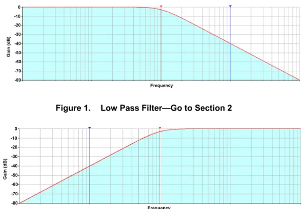
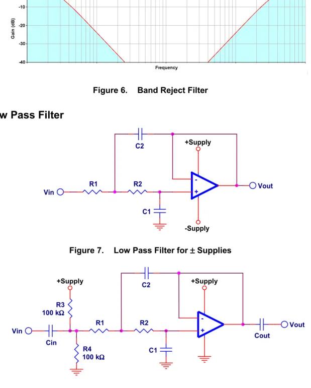
Ready? Let’s design the filter. Pick the filter type from one of the following 6 options that represents the frequencies to be passed (shaded area):
Figure 1. Low Pass Filter—Go to Section 2
Figure 3. Narrow (Single Frequency) Band Pass—Go to Section 4
Figure 4. Wide Band Pass —Go to Section 5
Figure 6. Band Reject Filter
2 Low Pass Filter
R2 Vin
-Supply C1
C2
-+ R1
+Supply
Vout
Figure 7. Low Pass Filter for ±±±± Supplies
+Supply
-+ +Supply
R4 100 kΩΩΩΩ
R3 100 kΩΩΩΩ
Cout Vin
C1 Cin
C2
Vout R2
R1
Figure 8. Low Pass Filter for a Single Supply
Design Procedure:
• Pick C1: __________
• Calculate R1 and R2 =
Frequency
*
C
*
*
1
2
2
1
π
: __________ (pick a standard value fromAppendix A).
For the single supply case only:
• Calculate Cin = Cout = 100 to 1000 times C1 (not critical): __________
DONE
3 High Pass Filter
Vout C2 R1 C1 Vin -Supply -+ +Supply R2
Figure 9. High Pass Filter for ±±±± Supplies
R1 R2 +Supply C1 Vout -+ C2 Cout
+Supply / 2 Vin
Figure 10. High Pass Filter for a Single Supply
Design Procedure:
• Pick C1 = C2: __________
• Calculate R1:
Frequency
*
C
*
*
1
2
1
π
: ___________ (pick a standard value from• Calculate R2:
Frequency
*
C
*
*
1
2
2
1
π
: __________ (pick a standard value fromAppendix A).
For the single supply case only:
• Calculate Cout = 100 to 1000 times C1 (not critical): __________
DONE
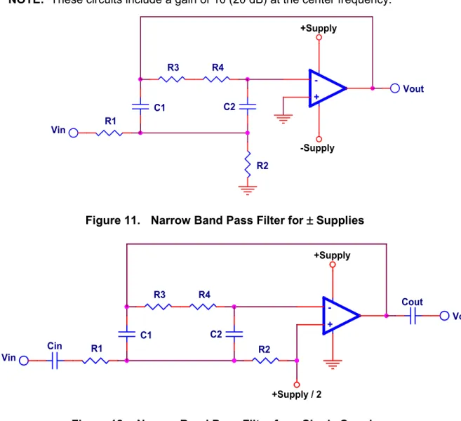
4 Narrow (Single Frequency) Band Pass Filter
NOTE: These circuits include a gain of 10 (20 dB) at the center frequency.
R4
C2
+Supply
-Supply
R1
C1
-+
R2 Vin
Vout R3
Figure 11. Narrow Band Pass Filter for ±±±± Supplies
R3
Cout
-+
Cin
C2 R1
R4
C1
R2
Vout +Supply
+Supply / 2 Vin
Figure 12. Narrow Band Pass Filter for a Single Supply
Design Procedure:
• Calculate R1 = R4: Frequency * C * * 1 2 1
π : ___________ (pick a standard value from
Appendix A).
• Calculate R3 = 19 * R1
• Calculate R2 =
19 1 R
For the single supply case only:
• Calculate Cin = Cout = 100 to 1000 times C1 (not critical): __________
DONE
5 Wide Band Pass Filter
NOTE: The start and ending frequencies of the band should be at least five times different.
R2 +Supply -Supply -Supply -+ C1 C2 R2 C1 Vin C2 -+ R1 R1 +Supply Vout
Figure 13. Wide Band Pass Filter for ±±±± Supplies
C1 Cout C2 R1 R2 R1 C2 C1 -+
+Supply / 2
-+
Vin
R2 +Supply +Supply
Vout
Figure 14. Wide Band Pass Filter for a Single Supply
Design Procedure:
• Go to Section 2, and design a low pass filter for the high end of the band.
• For the single supply case only:
• Calculate Cin = Cout = 100 to 1000 times C1 in the low pass filter section (not critical): __________
DONE
6
Notch (Single Frequency Rejection) Filter
R3
-+
R2
Vout
-Supply
R4 R1
-Supply
-+ C2
R6 100 kΩΩΩΩ R5 100 kΩΩΩΩ C1
+Supply
Vin
+Supply
R4 -+
R3
+Supply / 2 R1
+Supply
R2 C1
+Supply
R5 100 kΩΩΩΩ C2
Vin
Vout
-+ Cin
Cout
R6 100 kΩΩΩΩ
Figure 16. Narrow Band Pass Filter for a Single Supply
Design Procedure:
• Pick C1 = C2: __________
• Calculate R3 = R4:
Frequency *
C *
* 1
2
1
π : ___________ (pick a standard value from
Appendix A).
• Calculate R1 = R2 = 20 * R3
• For the single supply case only:
• Calculate Cin = Cout = 100 to 1000 times C1 (not critical): __________
DONE
7
Band Reject Filter
+Supply R2
100 kΩΩΩΩ -+ C1 +Supply R1 Vin C2 -+ -Supply C1 +Supply C2
100 kΩΩΩΩ
Vout
-+ R2
-Supply 100 kΩΩΩΩ
R1
-Supply
Figure 17. Band Reject Filter for ±±±± Supplies
C1
100 kΩΩΩΩ
-+
+Supply / 2 100 kΩΩΩΩ 100 kΩΩΩΩ Cin
C1
R2
+Supply / 2 R1 Cout +Supply +Supply C2 Vout R1 -+ Vin +Supply R2 C2 -+
Design Procedure:
• Go to Section 3, and design a high pass filter for the low end of the upper band.
• Go to Section 2, and design a low pass filter for the high end of the lower band.
• For the single supply case only:
• Calculate Cin = Cout = 100 to 1000 times C1 in the low pass filter section (not critical): __________
Appendix A—Standard Resistor and Capacitor Values
E-12 Resistor / Capacitor Values
1.0, 1.2, 1.5, 1.8, 2.2, 2.7, 3.3, 3.9, 4.7, 5.6, 6.8, and 8.2; multiplied by the decade value.
E-24 Resistor / Capacitor Values
1.0, 1.1, 1.2, 1.3, 1.5, 1.6, 1.8, 2.0, 2.2, 2.4, 2.7, 3.0, 3.3, 3.6, 3.9, 4.3, 4.7, 5.1, 5.6, 6.2, 6.8, 7.5, 8.2, and 9.1; multiplied by the decade value.
E-96 Resistor Values
Appendix B—Filter Notes (for the More Technically Minded)
Low Pass Filter
The filter selected is a unity gain Sallen-Key filter, with a Butterworth response characteristic. Numerous articles and books describe this topology.
High Pass Filter
The filter selected is a unity gain Sallen-Key filter, with a Butterworth response characteristic. Numerous articles and books describe this topology.
Narrow Band Pass Filter
The filter selected is a modified Deliyannis filter. The Q is set at 10, which also locks the gain at 10, as the two are related by the expression:
Gain Q
R R R
= = ⋅ +
1 2
4 3
A higher Q was not selected, because the op amp gain bandwidth product can be easily reached, even with a gain of 20 dB. At least 40 dB of headroom should be allowed above the center frequency peak. The op amp slew rate should also be sufficient to allow the waveform at the center frequency to swing to the amplitude required.
Wide Band Pass Filter
This is nothing more than cascaded Sallen-Key high pass and low pass filters. The high pass comes first, so energy from it that stretches to infinite frequency will be low passed.
Notch Filter
This is the Fliege Filter topology, set to a Q of 10. The Q can be adjusted independently from the center frequency by changing R1 and R2. Q is related to the center frequency set resistor by the following:
3 2
2
1 R *Q*R
R = =
The Fliege filter topology has a fixed gain of 1.
The only real possibility of a problem is the common mode range of the bottom amplifier in the single supply case.
Band Reject Filter
Texas Instruments Incorporated and its subsidiaries (TI) reserve the right to make corrections, modifications, enhancements, improvements, and other changes to its products and services at any time and to discontinue any product or service without notice. Customers should obtain the latest relevant information before placing orders and should verify that such information is current and complete. All products are sold subject to TI’s terms and conditions of sale supplied at the time of order acknowledgment.
TI warrants performance of its hardware products to the specifications applicable at the time of sale in accordance with TI’s standard warranty. Testing and other quality control techniques are used to the extent TI deems necessary to support this warranty. Except where mandated by government requirements, testing of all parameters of each product is not necessarily performed.
TI assumes no liability for applications assistance or customer product design. Customers are responsible for their products and applications using TI components. To minimize the risks associated with customer products and applications, customers should provide adequate design and operating safeguards.
TI does not warrant or represent that any license, either express or implied, is granted under any TI patent right, copyright, mask work right, or other TI intellectual property right relating to any combination, machine, or process in which TI products or services are used. Information published by TI regarding third–party products or services does not constitute a license from TI to use such products or services or a warranty or endorsement thereof. Use of such information may require a license from a third party under the patents or other intellectual property of the third party, or a license from TI under the patents or other intellectual property of TI.
Reproduction of information in TI data books or data sheets is permissible only if reproduction is without alteration and is accompanied by all associated warranties, conditions, limitations, and notices. Reproduction of this information with alteration is an unfair and deceptive business practice. TI is not responsible or liable for such altered documentation.
Resale of TI products or services with statements different from or beyond the parameters stated by TI for that product or service voids all express and any implied warranties for the associated TI product or service and is an unfair and deceptive business practice. TI is not responsible or liable for any such statements.
Mailing Address:
Texas Instruments Post Office Box 655303 Dallas, Texas 75265