© 2014 Science Publications
doi:10.3844/jcssp.2014.1130.1134 Published Online 10 (7) 2014 (http://www.thescipub.com/jcs.toc)
Corresponding Author: Bommi, R.M., Department of ECE, Sathyabama University, Chennai, India
ALL OPTICAL IMPLEMENTATION OF HIGH SPEED
AND LOW POWER REVERSIBLE FULL ADDER
USING SEMICONDUCTOR OPTICAL AMPLIFIER
BASED MACH-ZEHNDER INTERFEROMETER
1
Bommi, R.M.
and
2S. Selvakumar Raja
1
Department of ECE, Sathyabama University, Chennai, India
2Department of ECE, Arunai college of Engineering, Tiruvannamalai, India
Received 2013-12-16; Revised 2013-12-17; Accepted 2014-02-12
ABSTRACT
In the recent years reversible logic design has promising applications in low power computing, optical computing, quantum computing. VLSI design mainly concentrates on low power logic circuit design. In the present scenario researchers have made implementations of reversible logic gates in optical domain for its low energy consumption and high speed. This study is all about designing a reversible Full adder using combination of all optical Toffoli and all optical TNOR and to compare it with the Full adder designed using all optical Toffoli gate in terms of optical cost. All optical TNOR gate can work as a replacement of existing NAND based All optical Toffoli Gate (TG). The gates are designed using Mach-Zehnder Interferometer (MZI) based optical switch. The proposed system is developed with the basic of reversibility to design all optical full Adder implemented with CMOS transistors. The design is efficient in terms of both architecture and in power consumption.
Keywords: All Optical Toffoli Gate, All Optical TNOR, Optical Cost, MZI
1. INTRODUCTION
Reversible logic is emerging as a promising computing paradigm among the up-coming technologies. The Reversible logic has applications in Nano computing, quantum dot cellular automata, optical computing, Reversible circuits does not lose information while performing the computations. In reversible logic there exists a unique one to one mapping between the input and output vectors. The unused outputs are used to maintain the reversibility of reversible circuits and are referred as the garbage outputs. The inputs that are regenerated at the outputs are not considered as the garbage outputs. The constant inputs in the reversible circuits are called the ancilla inputs.
A photon can provide unmatched high speed and can store the information in a signal of zero mass. These properties of photon have attracted the attention of researchers to implement the reversible logic gates in all
logic gate. The optical cost of a reversible logic gate is defined as the number of MZI switches used in its all optical implementation. This design forms the basis for different quantum ALU and embedded processors (Murugesan and Keppanagounder, 2014).
2. BASICS OF EXISTING ALL OPTICAL
REVERSIBLE NAND LOGIC GATES
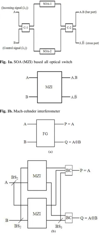
The Mach-Zehnder Interferometer (MZI) based optical switch is widely used to implement reversible logic gates (Maity et al., 2009). The design of all optical MZI switch is shown in Fig. 1a. The all optical MZI switch can be designed using 2 Semiconductor Optical Amplifier (SOA-1, SOA-2) and two couplers (C-1, C-2) (Kotiyal et al., 2012). The operating principle of MZI based all optical switch can be explained as follows.
In MZI switch, there are two inputs ports A and B and two output ports called as bar port and cross port, correspondingly as shown in Fig. 1b. The optical signal coming at port B is considered as the control signal (λ2) and the optical signal coming at port A is considered as incoming signal (λ1). The working of a MZI can be explained as: (i) when there is an incoming signal at port A and the control signal at port B then there is a light present at the output bar port and no light is present at the output cross port, (ii) in the absence of control signal at input port B and there is a incoming signal at input port A, then the outputs of MZI are switched and results in the presence of light at the output cross port and no light at the bar port. We consider no light or absence of light as the logic 0 . This behavior of MZI based all optical switch can be written as Boolean functions having inputs to outputs mapping as (A, B) to (P = AB, Q = AB¯ ), where A(incoming signal), B(control signal) are the inputs of MZI and P(Bar Port), Q(Cross Port) are the outputs of MZI, respectively. The block diagram of MZI based all optical switch is shown in Fig. 2. The optical cost and the delay ( ) of MZI based all optical switch is considered as unity (Donald and Niraj, 2008).
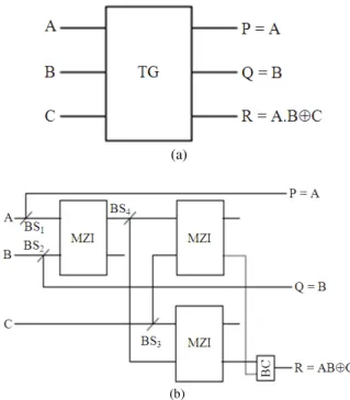
2.1. All Optical Feynman Gate
The Feynman Gate (FG) is a 2 inputs and 2 outputs reversible gate. It has the mapping (A, B) to (P = A, Q = A⊕ B) where A, B are the inputs and P, Q are outputs, correspondingly (Thapliyal and Srinivas, 2012). A Feynman gate can be implemented using 2 MZI based all optical switch, 2 Beam Combiner (BC) and 2 Beam Splitter (BS) in all optical reversible computing.
Fig. 1a. SOA (MZI) based all optical switch
Fig. 1b. Mach-zehnder interferometer
(a)
(b)
Fig. 2. (a) Feynman gate (b) All optical Implementation of FG
splitter simply splits the beams into two optical beams, hence researchers do not consider them in the optical cost and the delay calculations. Figure 2 shows the block diagram and the all optical implementation of the Feynman gate. As the Feynman gate can be implemented using 2 MZI based optical switches thus the optical cost of Feynman gate is considered as 2 and delay of the optical Feynman gate is considered as 1 .
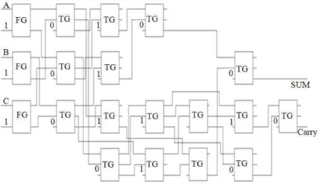
2.2. All Optical Toffoli Gate
The Toffoli gate(TG) is a 3 inputs and 3 outputs reversible gate. The inputs to outputs mapping of a Toffoli gate is (A, B, C) to (P = A, Q = B, R = AB⊕C), where A, B, C are the inputs and P, Q, R are the outputs, respectively (Haghparast and Navi, 2008). Figure 3 shows the block diagram and all optical implementation of Toffoli gate. The Toffoli gate work as a NAND gate when the value of input signal C is set to one. An all optical Toffoli gate can be implemented using 3 MZI based all optical switches, 1 Beam Combiner (BC) and 4 beam splitters.
The optical cost of Toffoli gate is considered as 3 as the Toffoli gate can be implemented using 3 MZI based all optical switches. The Toffoli gate has a delay of 2 as two MZI switches out of three MZI switches work in parallel.
(a)
(b)
Fig. 3. (a) Toffoli gate (b) Optical Implemention of TG gate
3. BASICS OF EXISTING ALL OPTICAL
REVERSIBLE NOR GATE
The all optical TNOR Gate (TNORG) can work as a replacement of existing NAND based all optical Toffoli gate. The TNORG can perform NOR based implementation of reversible Boolean functions in optical computing domain with reduced optical cost and delay. The all optical TNORG is a 3×3 reversible logic gate having inputs to outputs mapping as (A, B, C ) to (P = A, Q = B, R = (A+B)⊕c), where A, B, C are the inputs and P, Q, R are outputs, respectively. Figure 4 shows the block diagram and the optical implementation of all optical TNORG.
The all optical TNORG will work as a NOR gate when the value of input signal C is 1. The all optical TNORG can be implemented using 2 MZI based switches, 4 Beam Splitters (BS) and 2 Beam Combiners (BC). The optical cost of TNORG is considered as 2, since its optical implementation requires 2 MZI based switches. The all optical TNORG has delay of 1 as in its optical design two MZI switches works in parallel.
(a)
(b)
4. PROPOSED REVERSIBLE FULL
ADDER CIRCUITS
Three types of reversible full adders are proposed. The proposed reversible full adder using all optical TG is shown in Fig. 5. It uses 16 all optical TG and 3 FG. The calculation of optical cost for this circuit is as follows: Optical Cost (full adder) = Optical cost of Feynman gate * No. of all optical Feynman gate + Optical cost of TOFFOLI gate * No of all Optical TOFFOLI gate = 2*3+3*16 = 54. The delay of all optical implementation using Toffoli gate is 13 .
The proposed reversible full adder using all optical TNORG is shown in the Fig. 6. It uses 16 all optical TNORG and 3 FG. The calculation of optical cost for this
circuit is as follows: Optical Cost (full adder) = Optical cost of Feynman gate * No. of all optical Feynman gate + Optical cost of all optical TNOR gate * No of all Optical TNOR gate = 3*2+16*2 = 38. The delay of all optical implementation using TNOR gate is 8 .
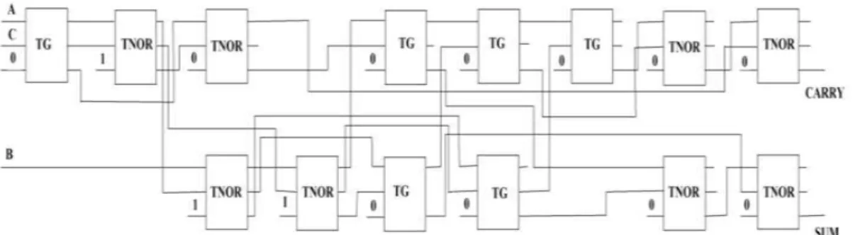
The proposed reversible full adder using combination of all optical TG and TNORG is shown in Fig. 7. It uses 6 all optical TG and 8 all optical TNORG. The calculation of optical cost for this circuit is as follows: Optical Cost (full adder) = Optical cost of Toffoli gate * No. of all optical Toffoli gate + Optical cost of TNOR gate * No of all Optical TNOR gate = 6*3+8*2 = 34. The delay of all optical implementation reversible full adder using Toffoli and TNOR gate is 13 .
Fig. 5. Proposed Reversible full adder using all optical Toffoli Gate
Fig. 7. Proposed Reversible full adder using all optical Toffoli and TNOR Gate
Table 1. Comparison table for optical cost and delay of all optical reversible NAND logic and all optical reversible Reversible gate Optical cost Delay
Toffoli gate 3 2∆
Proposed TNOR gate 2 1∆
Feynman gate 2 1∆
Table 2. Optical cost and delay comparison
Full adder Optical cost Delay All optical TG gate 54 13∆ All optical TNOR gate 38 8∆ TG and TNOR gate 34 13∆
Table 3. Power comparison
Full adder Average power All optical TG gate 6.3252E-06 All optical TNOR gate 3.6012E-06 TG and TNOR gare 3.2918E-06
5. CONCLUSION
The circuit is simulated with CMOS FET libraries which are readily available in Spice. Comparison of optical cost and delay for reversible gates is shown in Table 1. TNOR gate showed improved optical cost and delay compared to all optical Tofolli gate. Table 2 shows the optical cost, delay comparison of full adder using all optical Toffoli gate, TNOR gate and combination of all optical Toffoli and TNOR gate. The full adder implemented using the combination of all optical TG and TNORG proved to have reduced optical cost as compared to other two categories. Table 3 shows the average power comparison of Full adder using all optical Toffoli gate, TNOR gate and combination of all optical Toffoli and TNOR gate. The implementation of Full adder using the combination of all optical TG and TNORG proved to have reduced average power as compared to other two categories. In conclusion the combination of all optical TG and TNORG can be used to implement functions with reduced optical cost and average power consumed in a circuit.
6. REFERENCES
Donald, J. and K. Niraj, 2008. Reversible logic synthesis with fredkin and peres gates. ACM J. Emerg. Technol. Comput. Syst., 4: 1-19. DOI: 10.1145/1330521.1330523
Haghparast, M. and K. Navi, 2008. A novel reversible BCD adder for nanotechnology based systems. Am. J. Applied Sci., 5: 282-288. DOI:
10.3844/ajassp.2008.282.288
Kotiyal, S., H. Thapliyal and N. Ranganathan, 2012. Mach-Zehnder interferometer based all optical reversible nor gates. Proceedings of the IEEE Computer Society Annual Symposium, Aug. 19-21, IEEE Xplore Press, Amherst, MA., pp: 19-21. DOI: 10.1109/ISVLSI.2012.72
Maity, G.K., T. Chattopadhyay, J.N. Roy and S.P. Maity, 2009. All-optical reversible multiplexer. Proceedings of the 4th International Conference on Computers and Devices for Communication, Dec.14-16, IEEE Xplore Press, Kolkata, pp: 1-3. Murugesan, P. and T. Keppanagounder, 2014. Design of
optimal carry skip adder and carry skip BCD adder using reversible logic gates. J. Comput. Sci., 10: 723-728. DOI:10.3844/jcssp.2014.723.728
Thapliyal, H. and M.B Srinivas, 2012. A novel reversible tsg gate and its application for designing reversible carry look-ahead and other adder architectures. Proceedings of the 10th Asia-Pacific Computer Architecture Conference, Oct. 24-26, Springer Berlin Heidelberg, Singapore, pp: 805-817. DOI: 10.1007/11572961_66