RUI MANUEL LEITÃO SANTOS TAVARES
TIME-DOMAIN OPTIMIZATION OF
AMPLIFIERS BASED ON
DISTRIBUTED GENETIC ALGORITHMS
Thesis presented in partial fulfillment of the
requirements for the degree of Doctor of
Philosophy in the subject of Electrical and
Computer Engineering.
v
ACKNOWLEDGEMENTS
Several persons have contributed to the success of this work. To all of them I wish to express my deepest gratitude and thanks. In particular I would like to thank: Prof. Nuno Paulino, my supervisor, to whom I wish to express my sincere gratitude. His continuous guidance, encouragement, support, and valuable discussions have granting me the opportunity to pursue this work. Prof. João Goes, my co-supervisor for always supporting the project and for sharing his skills, passion and experience in analog circuit design.
Also, I am grateful to Professor A. Steiger-Garção, president of the Departamento de Engenharia Electrotecnica da Faculdade de Ciências de Technologia da Universidade Nova de Lisboa, for his friendship, understanding, and helped me to pursue my academia goals.
To the Electrical and Engineering Department (DEE) staff and colleagues, big thanks for the friendship, support and brief sessions of chat to clear a bit of the stress.
To my colleagues at the Microelectronics and Circuits (MESP) of the Centre for Technology and Systems (CTS), at UNINOVA, for support and friendship, notably, Michael Figueiredo, Edinei Santin and Bruno Esperança that used and tested the platform in their research works, e.g. Ph. D., and, after, allowed me to use the respective results in this document.
vii
ABSTRACT
The work presented in this thesis addresses the task of circuit optimization, helping the designer facing the high performance and high efficiency circuits demands of the market and technology evolution. A novel framework is introduced, based on time-domain analysis, genetic algorithm optimization, and distributed processing.
The time-domain optimization methodology is based on the step response of the amplifier. The main advantage of this new time-domain methodology is that, when a given settling-error is reached within the desired settling-time, it is automatically guaranteed that the amplifier has enough open-loop gain, AOL, output-swing (OS), slew-rate (SR), closed loop bandwidth and closed loop stability. Thus, this simplification of the circuit‟s evaluation helps the optimization process to converge faster. The method used to calculate the step response expression of the circuit is based on the inverse Laplace transform applied to the transfer function, symbolically, multiplied by 1/s (which represents the unity input step). Furthermore, may be applied to transfer functions of circuits with unlimited number of zeros/poles, without approximation in order to keep accuracy. Thus, complex circuit, with several design/optimization degrees of freedom can also be considered. The expression of the step response, from the proposed methodology, is based on the DC bias operating point of the devices of the circuit. For this, complex and accurate device models (e.g. BSIM3v3) are integrated. During the optimization process, the time-domain evaluation of the amplifier is used by the genetic algorithm, in the classification of the genetic individuals. The time-domain evaluator is integrated into the developed optimization platform, as independent library, coded using C programming language.
The genetic algorithms have demonstrated to be a good approach for optimization since they are flexible and independent from the optimization-objective. Different levels of abstraction can be optimized either system level or circuit level. Optimization of any new block is basically carried-out by simply providing additional configuration files, e.g. chromosome format, in text format; and the circuit library where the fitness value of each individual of the genetic algorithm is computed.
viii
(MPI). It is demonstrated that the distributed processing reduced the optimization run-time by more than one order of magnitude.
ix
SUMÁRIO
O trabalho apresentado nesta dissertação aborda a tarefa do dimensionamento de circuitos (em concreto, amplificadores), e pretende ajudar o engenheiro no projecto de circuitos, automatizando parte desta mesma tarefa. A nova metodologia de optimização é baseada na resposta temporal do amplificador ao escalão e utiliza algoritmos genéticos com processamento distribuído.
A principal vantagem da análise da resposta ao escalão, é o facto de um dado tempo de estabelecimento, da resposta, dentro de um dado erro de estabelecimento é suficiente para garantir que o circuito amplificador tem suficiente ganho em malha aberta, “output-swing” (OS), “slew-rate” (SR), e através da resposta ao escalão, concluir sobre a estabilidade quando realimentado em malha fechada. Esta simplificação na avaliação dos circuitos ajuda o processo de optimização a convergir mais rapidamente. O procedimento para determinação da expressão da resposta ao escalão utiliza a transformada inversa de Laplace, aplicada à função de transferência, do circuito, multiplicada, simbolicamente, por 1/s (que representa o escalão à entrada do circuito). Mais, este procedimento pode ser aplicado a funções de transferência com um número ilimitado de zeros e pólos, sem necessidade de utilizar qualquer tipo de aproximação, evitando perda de precisão. Desta forma, é possível optimizar circuitos complexos, com vários graus de liberdade. O cálculo da resposta ao escalão, utilizando a expressão, descrita anteriormente, é baseado nos valores do ponto de funcionamento em repouso (PFR) do circuito. Neste contexto são utilizados modelos de transístores complexos e precisos (e.g. BSIM3v3) para calcularo PFR. Este método de avaliação de circuitos, baseado no domínio do tempo é utilizado, durante o processo de optimização, pelo algoritmo genético, para classificar, ordenar e, posteriormente, gerar novas populações de indivíduos (circuitos). O bloco de software responsável pela avaliação dos circuitos, no domínio do tempo, é uma biblioteca independente, codificada utilizando linguagem de programação C. Esta biblioteca é integrada na plataforma de optimização desenvolvida.
x
O emprego do processamento distribuído/paralelo diminui o tempo de processamento, o estudo de circuitos mais complexos e a utilização de modelos de transístores mais precisos. A comunicação entre os nós de processamento remoto e o servidor baseia-se no conceito de Message Passing Interface (MPI). É demonstrado que a utilização de processamento distribuído reduz o tempo de optimização, em mais do que uma ordem de grandeza.
xi
KEYWORDS
Time-Domain Optimization
Amplifiers
Distributed Processing
Message Passing Interface
Genetic Algorithms
Computer-Aided Design
Integrated Circuits Design Automation
PALAVRAS-CHAVE
Optimização no Domínio do Tempo
Amplificadores Analógicos
Processamento Distribuído
« Message Passing Interface »
Algoritmos Genéticos
Desenho Assistido por Computador
xiii
ABBREVIATIONS
DAC Digital-to-Analog Converter
ADC Analog-to-Digital Converter
MADC Multiplying Analog-to-Digital Converter MOS Metal–Oxide–Semiconductor
MOSFET Metal–Oxide–Semiconductor Field-Effect-Transistor
PMOS P-channel MOSFET
NMOS N-channel MOSFET
CMOS Complementary Metal–Oxide–Semiconductor BiCMOS Bipolar Complementary Metal-Oxide Semiconductor OPAMP Operational Amplifier
OTA Operational Transconductance Amplifier SC Switched-Capacitor
DC Direct Current
IEEE Institute of Electrical & Electronics Engineers
SoC System-On-Chip
IC Integrated Circuit
AWE Asymptotic Wave Evaluation
SPICE Simulation Program with Integrated Circuit Emphasis BSIM Berkeley Short-Channel IGFET Model
EKV Mathematical model of MOSFET transistor BSP Behavioral Signal Path
AMD Advanced Micro Devices AMS Austrian Micro Systems
UMC United Microelectronics Corporation CAD Computer Aided Design
EDA Electronic Design Automation IP Intellectual Property
AI Artificial Intelligence
SA Simulated Annealing
GA Genetic Algorithms
GP Geometrical Programming
xiv
DSP Digital Signal Processing GBW Gain-Bandwidth Product CMRR Common-Mode Rejection Ratio PSRR Power Supply Rejection Ratio SNR Signal-to-Noise Ratio
THD Total Harmonic Distortion UGB Unity-Gain Bandwidth UGF Unity-Gain Frequency
RF Radio Frequency
GUI Graphical User Interface VLSI Very Large Scale Integration
VHSIC Very-High-Speed Integrated Circuit VHDL VHSIC Hardware Description Language DRC Design Rule Check
LVS Layout Versus Schematic
UNIX Uniplexed Information and Computing System LINUX Linus Torvald's UNIX (flavor of UNIX for PCs) GNU GNU‟s not UNIX!
GPL GNU Public License
EDIF Electronic Design Interchange Format CIF Caltech Intermediate Form
GDSII Graphic Database System II
xv
TABLE OF CONTENTS
ACKNOWLEDGEMENTS ________________________________________________ v
ABSTRACT __________________________________________________________ vii
SUMÁRIO __________________________________________________________ ix
KEYWORDS _________________________________________________________ xi
ABBREVIATIONS ____________________________________________________ xiii
TABLE OF CONTENTS _________________________________________________ xv
LIST OF FIGURES _____________________________________________________xix
LIST OF TABLES _____________________________________________________xxiii
1 Introduction ______________________________________________________ 1
1.1 Analog Design Flow _________________________________________________ 4
1.1.1 Circuit-level design ________________________________________________________ 5
1.2 Motivation ________________________________________________________ 6
1.3 Scope of this Thesis _________________________________________________ 8
1.4 Main Research Contributions _________________________________________ 8
1.5 Outline __________________________________________________________ 10
2 Computer Aided Design of Analog Circuits ____________________________ 13
2.1 Circuit Sizing/Optimization __________________________________________ 13
2.1.1 Knowledge-based approaches ______________________________________________ 14 2.1.2 Optimization-based approaches ____________________________________________ 16
2.2 Comparative Summary of the Approaches _____________________________ 27
2.2.1 Knowledge-based versus optimization-based __________________________________ 28 2.2.2 Summary of optimization-based approaches __________________________________ 28
2.3 Brief Considerations about Layout Automation _________________________ 31
2.4 Open-Source Tools in Automation ____________________________________ 32
2.5 Proposed Work ___________________________________________________ 34
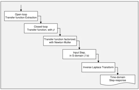
3 Time-Domain Optimization Methodology _____________________________ 37
3.1 The Main Steps of the Proposed Optimization Methodology _______________ 40
3.2 Time-Domain Step-Response ________________________________________ 41
3.3 Circuit Behavioral Signal Path Analysis_________________________________ 42
3.4 Equations (Level 2) of the MOS Transistors _____________________________ 45
xvi
3.4.4 Medium/high frequency small-signal equivalent model _________________________ 55 3.4.5 Linearization techniques for basic (single-device) MOS transistor circuits ___________ 59 3.4.6 Node isolation using Y-parameters __________________________________________ 65
3.5 Performance parameters of the amplifiers _____________________________ 69
3.5.1 Transfer function ________________________________________________________ 69 3.5.2 Gain-bandwith product ___________________________________________________ 70 3.5.3 Phase margin ___________________________________________________________ 70 3.5.4 Positive and negative power supply rejection ratio _____________________________ 71 3.5.5 Common mode rejection ratio _____________________________________________ 71 3.5.6 Slew rate _______________________________________________________________ 72 3.5.7 Noise (thermal and flicker) ________________________________________________ 72 3.5.8 Output swing ___________________________________________________________ 74 3.5.9 Settling time ____________________________________________________________ 74 3.5.10 Die area _____________________________________________________________ 75 3.5.11 Power dissipation______________________________________________________ 76
3.6 Transfer Function of the Amplifiers when Employed in Switched-Capacitor
Circuits ________________________________________________________________ 76
3.7 Time-Domain versus Frequency-Domain Optimization ____________________ 78
4 Platform Architecture and Genetic Algorithm Kernel ____________________ 81
4.1 Platform Architecture ______________________________________________ 82
4.1.1 Chromosome description file _______________________________________________ 84 4.1.2 Circuit performance parameters definition file ________________________________ 85 4.1.3 Genetic algorithm setup file _______________________________________________ 86
4.2 Genetic Algorithm Overview _________________________________________ 87
4.2.1 Structure of an individual __________________________________________________ 88 4.2.2 The classification process __________________________________________________ 89 4.2.3 The selection scheme _____________________________________________________ 92 4.2.4 The crossover operator ___________________________________________________ 94 4.2.5 The mutation operator____________________________________________________ 95
4.3 Circuit Library ____________________________________________________ 96
4.4 Highly Accurate Device Models ______________________________________ 98
4.5 Exported Statistics and Results _______________________________________ 98
4.6 Distributed Computing Version ______________________________________ 99
4.6.1 Classification, selection, crossover and mutation ______________________________ 100 4.6.2 The master computer process _____________________________________________ 101 4.6.3 The slave computer process ______________________________________________ 102 4.6.4 The message passing interface ____________________________________________ 104 4.6.5 Load distribution _______________________________________________________ 106 4.6.6 Distributed/Parallel environment performance _______________________________ 106
4.7 Conclusions _____________________________________________________ 108
5 Practical Design Examples and Silicon Results ________________________ 109
xvii 5.1.1 Circuit insight __________________________________________________________ 111 5.1.2 Adding a degree-of-freedom in a two-stage amplifier __________________________ 113 5.1.3 Design procedure and circuit optimization ___________________________________ 115 5.1.4 Post-optimization and simulation results ____________________________________ 118
5.2 Optimum Compensation and Sizing __________________________________ 121
5.2.1 Circuit insight __________________________________________________________ 122 5.2.2 Design procedure and circuit optimization ___________________________________ 124 5.2.3 Post-optimization and simulation results ____________________________________ 126
5.3 Two-Stage Amplifier Employing Gain-Boosting Techniques _______________ 128
5.3.1 Circuit insight __________________________________________________________ 128 5.3.2 Design procedure and circuit optimization ___________________________________ 132 5.3.3 Post-optimization and simulation results ____________________________________ 134
5.4 A Novel Two-Stage Self-Biased Inverter-Based Amplifier _________________ 135
5.4.1 Circuit insight __________________________________________________________ 139 5.4.2 Design procedure and circuit optimization ___________________________________ 141 5.4.3 Time-domain optimization ________________________________________________ 144 5.4.4 Simulation results _______________________________________________________ 146 5.4.5 Layout Design _________________________________________________________ 147
5.5 Experimental results ______________________________________________ 149
5.6 Conclusions _____________________________________________________ 153
6 Conclusions and Future Work ______________________________________ 155
6.1 Future Work _____________________________________________________ 157
Appendix A. Example of the Persisted Optimization Data ________________ 159
Appendix B. Example of the Optimized SPICE-like Netlist _________________ 161
xix
LIST OF FIGURES
Figure 1-1 Analog mixed signal system on chip[1] ... 1
Figure 1-2 Moore's law [8]: a) Number of transistors per processor versus year; b) Technology scaling verus year ... 3
Figure 1-3 Analog design flow ... 4
Figure 1-4 Analog circuit design ... 5
Figure 2-1 Knowledge-based circuit sizing ... 14
Figure 2-2 Optimization-based circuit sizing ... 17
Figure 2-3 Gradient-based search illustration ... 18
Figure 2-4 Equation-based circuit optimization ... 20
Figure 2-5 Simulation-based circuit optimization ... 22
Figure 2-6 Learning-based circuit optimization ... 24
Figure 2-7 Classification versus date of analog sizing implementations ... 29
Figure 3-1 Low-voltage two-stage cascode-compensated amplifier (biasing and CMFB circuitry not shown) ... 38
Figure 3-2 Steps of the proposed time-domain optimization methodology ... 40
Figure 3-3 Flow of the extraction of the time-domain step-response ... 41
Figure 3-4 Half of the circuit amplifier shown in Figure 3-1. ... 43
Figure 3-5 An example of the BSP of half of the circuit amplifier shown in Figure 3-1. ... 44
Figure 3-6 Symbols of MOS transistors: a) NMOS; b) PMOS ... 45
Figure 3-7 Symbols and conventions used in the large-signal model equations of MOS transistors: .... 46
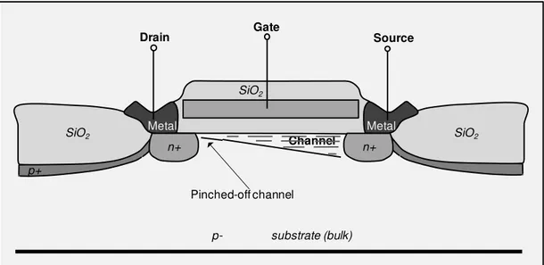
Figure 3-8 Cross-section of an NMOS transistor in the active region (saturation) ... 49
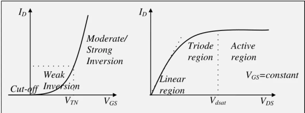
Figure 3-9 ID versus VDS characteristic of an NMOS transistor with channel-length modulation and with short-channel effects. ... 50
Figure 3-10 ID versusVGS and ID versusVDS characteristics of an NMOS transistor ... 51
Figure 3-11 Low-frequency small-signal equivalent model of an NMOS transistor ... 54
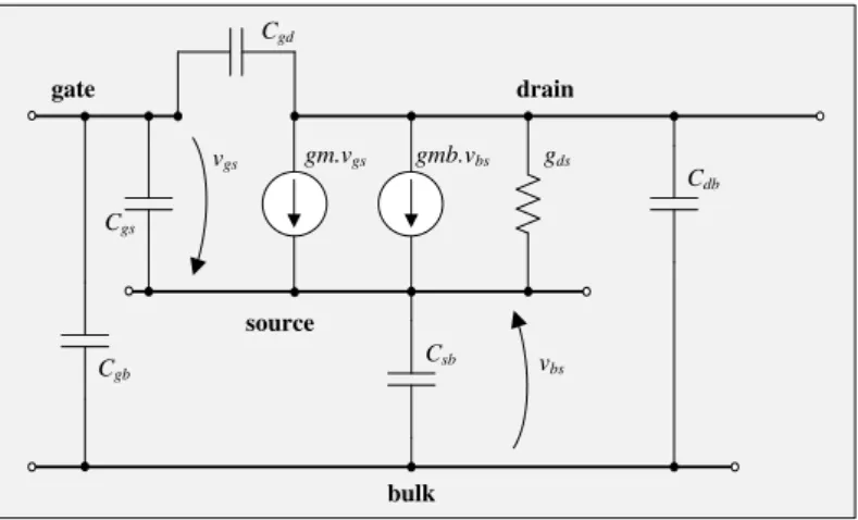
Figure 3-12 Medium/high frequency small-signal equivalent model of an NMOS transistor ... 55
Figure 3-13 Cross-section of an NMOS transistor with the most relevant associated capacitances [78] ... 56
Figure 3-14 Top-view of an NMOS transistor layout masks [78] ... 56
Figure 3-15 Parasitic capacitances versus gate-to-source voltage, vGS[78] ... 58
Figure 3-16 Common-source transistor: a) Symbol; b) Small signal equivalent model ... 60
Figure 3-17 Common-drain transistor: a) Symbol; b) Small signal equivalent model ... 60
Figure 3-18 Common-gate transistor: a) Symbol; b) Small signal equivalent model... 62
Figure 3-19 Signal-transistor: a) Symbol; b) Small signal equivalent model ... 62
Figure 3-20 Current-source transistor: a) Symbol; b) Small signal equivalent model ... 63
Figure 3-21 Small signal equivalent model example of half of the circuit amplifier shown in Figure 3-1. ... 64
Figure 3-22 Simplified small signal equivalent model of the half of the circuit amplifier shown in Figure 3-1... 65
Figure 3-23 Y-Equivalent two port showing independent variables V1 and V2 ... 66
Figure 3-24 Y-paramenters of a capacitor: a) Capacitor; b) Y-Equivalent ... 66
Figure 3-25 Y-paramenters of a conductance: a) Conductance; b) Y-Equivalent ... 67
Figure 3-26 Y-paramenters of a transconductance, which controller-voltage is V1: ... 68
Figure 3-27 Y-paramenters of a transconductance, which controller-voltage is given by (other) voltage, VX: ... 68
xx
Figure 3-29 Transistor model for small-signal with noise source ... 73
Figure 3-30 Settling time representation ... 75
Figure 3-31 Switched-Capacitor S/H: a) Full circuit; b) Equivalent circuit on phase ϕ2 ... 77
Figure 3-32 Circuit diagram during phase ϕ2 ... 77
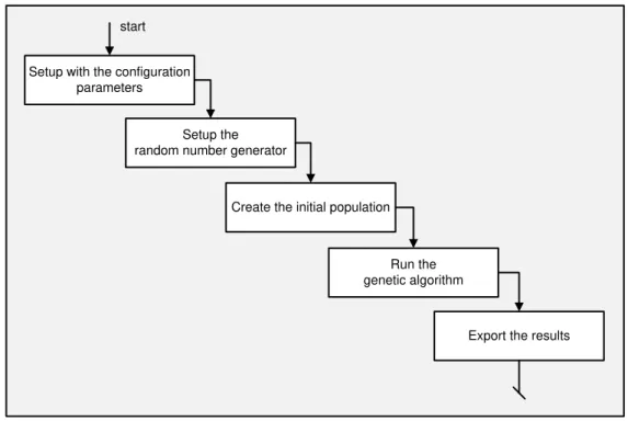
Figure 4-1 General architecture of the proposed optimization platform ... 82
Figure 4-2 Flow of the execution steps of the proposed platform ... 83
Figure 4-3 Chromosome description file snap shot ... 84
Figure 4-4 Circuit performance parameters definition file snap shot ... 85
Figure 4-5 Genetic algorithm setup file snap shot ... 86
Figure 4-6 Flow of the steps of the genetic algorithm ... 87
Figure 4-7 Format of a generic individual (chromosome) ... 88
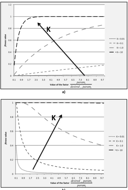
Figure 4-8 Behavior of the factor weighti in the maximize, a), and minimize, b), of fitness calculation 91 Figure 4-9 Behavior of the factor weighti in the target fitness calculation ... 91
Figure 4-10 Example of a Roulette system for the case of 5 individuals ... 93
Figure 4-11 Example of an unbalanced Roulette system for the case of 5 individuals ... 93
Figure 4-12 Rank system for 5 individuals ... 94
Figure 4-13 The crossover operator ... 94
Figure 4-14 The mutation operator ... 95
Figure 4-15 Flowchart of the calculation of the an individual fitness ... 96
Figure 4-16 Flowchart of a circuit evaluation ... 97
Figure 4-17 Example of an intermediate results printout ... 98
Figure 4-18 MPI Implementation of the distributed/parallel system ... 100
Figure 4-19 Master computer process of MPI implementation of the distributed/parallel system ... 101
Figure 4-20 Flowchart of the master process ... 102
Figure 4-21 Slave processes from MPI implementation of the distributed/parallel system ... 103
Figure 4-22 Flowchart of the slave process ... 104
Figure 4-23 MPI basic functions ... 105
Figure 4-24 MPI message format: master to slaves ... 105
Figure 4-25 MPI message format: slave to master ... 106
Figure 4-26 Speedup factor versus nr. of generations versus nr. of individuals ... 107
Figure 4-27 speedup factor versus nr. of computers (slaves) ... 107
Figure 5-1 Schematic of a conventional low-voltage two-stage amplifier ... 110
Figure 5-2 Behavioral Signal Path of half of the two-stage cascode amplifier shown in Figure 5-1 .... 112
Figure 5-3 Schematic of a two-stage cascode amplifier with regulated active-biasing ... 114
Figure 5-4 Schematic of an auxiliary folded-input OTA with CMFB transistor, M1Z ... 115
Figure 5-5 Behavioral Signal Path of half of the circuit cascode amplifier with active-biasing shown in Figure 5-3 ... 116
Figure 5-6 Format of the cascode amplifier with active-biasing chromossome ... 117
Figure 5-7 Zoom of the simulated settling-response of the conventional topology, Figure 5-1 (1st case), of the conventional topology with ICAS reduced by a factor of 4 (2 nd case) and of the proposed topology with ICAS reduced by 4 plus the auxiliary OTA, Figure 5-3 (3 rd case). ... 120
Figure 5-8 AC simulations (amplitude Bode diagrams) of the conventional topology (1st case), of the conventional topology with ICAS reduced by a factor of 4 (2nd case) and of the proposed topology with ICAS reduced by 4 plus auxiliary OTA (3rd case). ... 120
Figure 5-9 Schematic of a low-voltage two-stage cascode-compensated amplifier with a folded-cascode first-stage ... 121
Figure 5-10 Behavioral Signal Path of half of the amplifier with multiple compensation capacitors shown in Figure 5-9 ... 123
Figure 5-11 Format of the chromosome of the amplifier with multiple compensation capacitors ... 125
xxi
Figure 5-13 Evolution of the values of the compensation capacitances ... 127
Figure 5-14 Simulated settling-response of the topology with the selected compensation schema. ... 128
Figure 5-15 Schematic of the two-stage fully-differential gain-boosted OTA (biasing and CMFB circuitry not shown). ... 129
Figure 5-16 Behavioral Signal Path of half of the gain-boosted amplifier circuit shown in Figure 5-15130 Figure 5-17 Format of the two-stage gain-boosted amplifier chromossome ... 133
Figure 5-18 Simulated differential output response of the OTA, employing gain-boosting techniques. ... 134
Figure 5-19 Schematic of the new two-stage self-biased inverter-based amplifier ... 136
Figure 5-20 Schematics of the common-mode feedback circuits: a) SC network for 2nd stage (CMFB2); b) Continuous time CMFB circuit for input stage (CMFB1). ... 137
Figure 5-21 Behavioral signal path model of the two-stage self-biased inverter-based amplifier (for simplicity only half the circuit is shown) ... 138
Figure 5-22 Format of the chromossome of the two-stage self-biased inverter-based amplifier. ... 142
Figure 5-23 Simulated Bode diagrams of the two-stage self-biased inverter-based amplifier ... 146
Figure 5-24 Simulated step response of the two-stage self-biased inverter-based amplifier ... 146
Figure 5-25 Complete circuit floorplan layout ... 148
Figure 5-26 Layout of the proposed new two-stage self-biased inverter-based amplifier ... 148
Figure 5-27 Chip photograph with amplifier core area, CC, CCM, and CMFB2 ... 150
Figure 5-28 Measurement setup used for the amplifier characterization ... 150
Figure 5-29 Amplifier open-loop gain and phase Bode diagrams ... 152
xxiii
LIST OF TABLES
Table 2-1 Summary of analog sizing implementations ... 26 Table 3-1 Drain-current for MOSFET in large-signal and for low-frequency operation. ... 52 Table 3-2 Parasitic capacitances for MOS devices in the three main regions of operation. ... 61 Table 5-1 Optimized and post-simulated results for the conventional topology shown in Figure 5-1 . 119 Table 5-2 Optimized and post-simulated results for the proposed topology shown in Figure 5-3. ... 119 Table 5-3 Optimized and post-simulated results for the proposed topology shown in Figure 5-9 ... 127 Table 5-4 Optimized and post-simulated results for the amplifier topology shown in Figure 5-15. ... 134 Table 5-5 Optimized and post-simulated results of the circuit performance parameters, in the
1
Introduction
The electronic industry is increasingly focused on electronic devices that contain more and more features. Furthermore, these features are supposed to occupy the smallest possible volume, have the highest performance and as much autonomy (battery) as possible. A direct consequence of these factors is the design of circuits with higher complexity and integration of complete systems on a single chip (SoC), as exemplified in Figure 1-1. Furthermore, the market demands more circuits with better performance in a shorter development cycle, which makes the design cycle even more difficult and complex.
Figure 1-1 Analog mixed signal system on chip[1]
Although most of these features are intensively performed by digital circuits, the interaction with the real world is achieved by analog circuits. Since the signals in the real world are (still) analog signals. The interaction with these analog signals will, ultimately, be through analog-to-digital (A/D) and digital-to-analog (D/A) converters. Thus, it is necessary the coexistence of digital and analog circuitry in the same silicon die, if a SoC is to be implemented.
In the design of digital circuits, there are several tools that facilitate the development work [1]. For instance, digital circuits tolerate a fair amount of high order
m
P
DSP
RAM
DIGITAL
1 Introduction
2
effects and modeling errors that could ruin analog circuitry performance. Analog design requires tools that can deal with the superior complexity of the circuit behavior and device modeling. Although currently, analog circuits occupy less area in SoCs, they require the longest developing time and effort, and it is a task that must be performed by engineers with a high degree of knowledge [2]. As someone mentioned – “Analog design is somehow considered an art” [3].
Most of the time, in analog design, is spent in the optimization of the circuits. The non-linear relation between the dimensions of the components and the specifications of circuits is a complex problem. Since there are complex relations between input and output variables and since every design variable affects multiple performances. Each design can have multiple good solutions depending on the initial specifications. Thus, due to the huge design space, it becomes extremely difficult for human designers to manage a good compromise between all the specifications, and the design variables. Furthermore, it is necessary to study the sensitivity of the circuit to the manufacturing process, supply voltage, and temperature (PVT) variations. There is no systematical way of producing new analog designs. Even intellectual property (IP) reuse requires an expert designer or an expert system to map designs in new technologies. All the factors, previously mentioned, make analog design the bottleneck of SoC design. This is a problem because the percentage of analog design in SoC rises every year, based on predictions from the IBS Corporation[4].
Good design methodologies are needed to manage the complexity of analog design, in order to better explore the space of values of design variables and thus, reduce the effort, time and cost of production of new analog circuits.
1.1 Analog Design Flow
3 amplifier transfer function has several poles (some of them complex conjugated pairs) and zeros, making the amplifier design a complex task. Therefore the final design accuracy depends on the availability and quality of a powerful optimization algorithm. Another issue, when using deep sub-micrometer manufacturing technologies is the high order effects in the electrical characteristics of the transistors, e.g. short-channel effects. These are quite relevant and, only advanced models such as BSIM3v3 [5], BSIM4 [6] and PSP [7], can provide the required accuracy for calculating the I-V characteristics of the transistors.
Moore‟s law has stipulated that the number of transistors inside integrated circuits (IC) doubles every two years [8], as shown in the Figure 1-2. The problem is that the device size is reaching atom size, which imposes a limit to further scaling down of the transistors. Another issue is economical, it is expensive to build new IC, and the small size promotes high order effects and demands precise fabrication tools [9]. So, probably, the solution for circuit design innovation is on the Electronic Design Automation (EDA) side. It needs to came up with novel methodologies and tools to help better designing circuits and systems.
a)
b)
Figure 1-2 Moore's law [8]: a) Number of transistors per processor versus year; b) Technology scaling verus year
The work presented in this thesis addresses all this challenges, in particular, the problem of amplifier‟s optimization, describing a methodology based on the analysis, in
4004 8008 8080 8086 8088 286 386 486 Pentium Pentium Pro Pentium II Pentium III Pentium IV Pentium M Pentium D
Core 2 Duo Core 2 QuadQuad-Core Xenon
2300 9200 36800 147200 588800 2355200 9420800 37683200 150732800 602931200
1971 1974 1977 1980 1983 1986 1989 1992 1995 1998 2001 2004 2007 2010
L o g2 N u m b e r o f T ra n si st o rs Year 0,03125 0,0625 0,125 0,25 0,5 1 2 4 8 16
1971 1974 1977 1980 1983 1986 1989 1992 1995 1998 2001 2004 2007 2010
1 Introduction
4
the time domain, of the step response of the amplifier. This design methodology allows the analysis and optimization of complex topologies of amplifiers with transfer functions that can have an unlimited number of poles and zeros.
The optimization process uses a genetic algorithm with parallel/distributed processing, integrated with the code of the models of transistors, BSIM3v31. The
scientific community has been making an effort in this direction. A good study of techniques and tools to help the design of analog circuits is available in [2].
1.1
Analog Design Flow
The simplified view of the steps required to design an analog system is depicted in Figure 1-3.
Figure 1-3 Analog design flow
The global design inputs are: the analog function to be implemented and the specifications of the function. The first step is to determine a suitable architecture, which should meet the given specifications.
The process then continues by decomposing the architectures into high-level blocks. Each block is further decomposed into low-level block until the corresponding circuit level is reached. The verifications are carried out at each stage, providing the lower-level block specifications. A back-annotation is also executed backwards to the higher-level block, if necessary. At this point, optimization helps to choose the best blocks for the given set of specifications.
1
This model was adopted, rather the improved version BSIM4, simply because most of the
demonstrations were designed on a 130 nm CMOS technology. However, the extension for BSIM4 is relatively straightforward
Analog Function
Architecture Design
Circuit performance
parameters
Valid Redesign
Backannotation
Valid Redesign
Valid Redesign
Block Design
Device Sizing
Backannotation
Layout Valid Redesign
Backannotation
1.1 Analog Design Flow
5 After the building blocks are well established, they are mapped into circuit-level devices. Each device is sized properly to ensure that the circuit performs according to the respective block specifications. This task is a multi-variable optimization procedure that must meet multiple specifications.
Finally, the layout produces the different layers mask based on the device sizes. These plans are then sent to fabrication after exhaustive simulations of the extracted layout (XRC - Extracted Resistance and Capacitances).
During the design phases, successive verifications are carried out. In the case of failure, the respective design stage must be revised. These results can be used to improve the previous design stage (back-annotation). Also, depending on the severity of the failure, the design process can reverse several phases.
The focus of this work is mainly on circuit optimization. Therefore, the next section discusses in more detail the circuit-level sizing.
1.1.1
Circuit-level design
The circuit design is characterized by the sequence shown in Figure 1-4.
Figure 1-4 Analog circuit design
Based on the circuit performance parameters obtained from the block level design, the selection of the circuit topology takes place. The next step is the circuit instantiation, with circuit devices being sized. The circuit instance is evaluated and validated against the defined indicators. The design process continues to layout, if validation is succeeded, or, in case of failure, redesign is needed.
1.1.1.1 Topology Selection
The selection of the best topology should choose the best candidate that meet all the circuit performance parameters. This process can be based on previous design instances, or designer knowledge (in addiction to some key calculations), and/or rules of
Topology Selection
Circuit performance
parameters
resize
Circuit Sizing Circuit Validation Evaluation
1 Introduction
6
thumb. If the circuit validation fails, the amount of failure determines if only a circuit resize is needed or if the selection process should go back and select a more suitable topology. After the topology selection, the design continues with the component sizing.
1.1.1.2 Device Sizing
This task modifies the design variables in order to meet the circuit performance parameters. The design variables are the values and sizes of each transistor, capacitor and resistor. Some of these components might get their values directly from the specifications but the majority of the sizes must be computed, based on the topology and specifications.
The relation between design variables and circuit specifications is nonlinear. It is a multi-variable with a multiple objective function. These facts make it a complex task. On simple circuits, the process relies on designer knowledge and simple calculations, based on simplified (level 1 or 2) device equations. When considering more complex circuits, sub-micrometer technologies and state-of-the-art design demand, the design task cannot rely on simplified device models. Accurate methods and models involve more time and increased computation effort.
Next, validation is carried with a circuit simulator and the results are compared to the specifications. Most certainly, the first results do not meet the specifications, and thus, the devices must be resized. Even on simple circuits, the decision on what parameters to change is not trivial. Rules of thumb and the designer expertise could lead to a good hit. Nevertheless, with complex circuits, this task cannot be achieved by humans only. Some commercial simulators provide a functionality that sweeps circuit parameters and provide some insight about the parameter influence on circuit performance. Parameter sweep is done at the cost of several simulations, which is time and computational costly.
The sizing and validation cycle must succeed after some iteration, otherwise the redesign process back iterates to select a different topology. Topology selection is a key task to avoid redesign. In a worst case scenario, the topology selections do not provide an acceptable performance match; the specifications for the circuit are too tight and should be revised or, as an alternative, a different technology node should be selected.
1.2
Motivation
1.2 Motivation
7 performance parameters. Changing a design variable interferes with several performance parameters. Even if the relation between specifications, design performance parameters and design variables are well known, it is a complex operation for a human mind to take in account. For instance, in a given amplifier, changing a transistor width can improve the low frequency gain but, it may cause a decrease of the GBW value.
Even if it is possible to manage the circuit sizing complexity, handling the nonlinear relations and complex calculations, there is the problem of the design-to-fabrication time. The time-costly operations in circuit sizing do not leave much freedom to evaluate all the design space.
The complexity and the amount of variables involved in the sizing process, handled manually, without process and data integration, are error-prone.
To improve systems yield there are two well-disseminated methods that may be used combined: process corners and Monte Carlo simulations. The foundries provide set of the fabrication technology parameters, which include the nominal and the worst-case values. The values of the last set are derived from process corners. In each Monte Carlo simulation, the design and process parameter values are altered based on statistical distribution. Often, during sizing step, design variables calculations are simply based on nominal values of the fabrication process. The corner values and Monte Carlo simulations are only considered after the last sizing step that succeeded. As a consequence, the circuit design ends with a considerable number of time-costly simulations.
In summary, design tools need to be developed, to efficiently cope with the analog design bottlenecks. These include the following:
Decrease design time: the processing capacity of a computer is largely higher than a human, manually, designing a circuit;
Reduce cost: reducing the time on design will decrease the time designers spent on circuit sizing (design effort);
Decrease errors: integrating and automating the design process frees designers from routine tasks and decrease errors resulting from human intervention, which normally follows a trial-and-error approach;
1 Introduction
8
including process corners and Monte Carlo simulations. Thus both, the design performance and Yield are improved.
1.3
Scope of this Thesis
The main subject of this thesis is the study and application of new techniques and methods to enhance the circuit (amplifier) sizing and optimization stage of analog design flow. This contributes to the improvement of the design automation task of analog circuits.
The tool developed and described in this work is able to compute the size of devices to meet the performance specifications given for an amplifier, thus contributing to decrease the time-to-tape-out, and to first-pass success.
1.4
Main Research Contributions
Two major contributions can be highlighted in this work:
1. An optimization EDA platform for amplifiers based on genetic algorithms [10] and distributed processing [11], following an efficient time-domain equation-based/simulation-based approach. Furthermore, the developed optimization tool is fully based in open-source code [12].
2. This platform was successfully applied in particular, in the design of two-stage amplifiers in the following way:
I. how an extra degree-of-freedom can be added to the design space allowing enhanced performance [13];
II. how to achieve optimum compensation of two-stage amplifiers [14];
III. how to achieve a DC gain above 100 dB, with gain-boosting techniques and optimization [15];
IV. how to achieve a power efficiency figure-of-merit (FOM) in a new class A amplifier, comparable to similar amplifiers employing class AB output stage through the optimization of and inverter-based self-bias two-stage amplifier [16], [17]. This work was
1.4 Main Research Contributions
9 Moreover, the demonstration of the practical effectiveness of the developed EDA platform has been shown throughout the design of several energy-efficient pipeline [18] and two-stage algorithmic analog-to-digital converter (ADC)[15]. Some of these circuits have been, later on, laid out, prototyped and evaluated. Hence, the targeted design performance parameters of the designed amplifiers were indirectly confirmed in silicon though experimental evaluation of the ADC [19].
The main contributions of this work are focused on the suitability of novel methods and techniques for optimization of complex analog circuits, in particular, two-stage amplifiers: the genetic algorithms [20] as the base for optimization, time-domain for circuit analysis [14] and distributed processing [11] for platform performance enhancement. As research contribution and work assessment, four application examples were also published:
1. Optimization of amplifiers for a power-and-area efficient multiplying digital-to-analog converter (MDAC) [15];
2. Transistor sizing and compensation capacitance schema of multi-stage amplifiers [14];
3. Optimization of amplifiers for MDAC stages, low-voltage and low-power efficient high-speed moderate resolution pipelined ADC [18].
This research work has been translated into the following authored / co-authored publications:
• M. Figueiredo, R. Santos-Tavares, E. Santin, J. Goes, "A Two-Stage Fully-Differential Inverter-based Self-Biased CMOS Amplifier with High Efficiency", submitted by
invitation to IEEE Transactions on Circuits and Systems I (TCAS I), October 2010.
• E. Santin, M. Figueiredo, R. Tavares, J. Goes and L. B. Oliveira, “Fast-Settling Low-Power Two-Stage Self-Biased CMOS Amplifier Using Feedforward-Regulated Cascode
Devices”, to appear in the IEEE International Conference on Electronics Circuits and Systems
(ICECS), Athens, Greece, December 2010.
• M. Figueiredo, E. Santin, J. Goes, R. Santos-Tavares, G. Evans, "Two-Stage Fully-Differential Inverter-based Self-Biased CMOS Amplifier with High Efficiency", IEEE
International Symposium on Circuits and Systems, Paris, France, May 2010.
• R. Santos-Tavares, N. Paulino, J. Higino, J. Goes, J. P. Oliveira, " Optimization of
Multi-Stage Amplifiers in Deep-Submicron CMOS Using a Distributed/Parallel Genetic
Algorithm”, IEEE International Symposium on Circuits and Systems, Seattle, USA, May 2008.
1 Introduction
10
Mismatch-Insensitive MDAC”, IEEE International Symposium on Circuits and Systems,
Seattle, USA, May 2008.
• R. Santos-Tavares, N. Paulino, J. Goes, J. P. Oliveira, “Optimum Sizing and
Compensation of Two-Stage CMOS Amplifiers Based On a Time-Domain Approach",
IEEE International Conference on Electronics, Circuits and Systems, Nice, France, December
2006.
• R. Tavares, B. Vaz, J. Goes, N. Paulino and A. Steiger-Garção, "Design and
Optimization of Low-Voltage Two-Stage CMOS Amplifiers with Enhanced
Performance", IEEE International Symposium on Circuits and Systems, Bangkok, Thailand,
May 2003.
• B. Vaz, N. Paulino, J. Goes, R. Costa, R. Tavares and A. Steiger-Garção, “Design of Low-Voltage CMOS Pipelined ADC‟s using 1 pico-Joule of Energy per Conversion”,
IEEE International Symposium on Circuits and Systems, Arizona, USA, May 2002.
• B. Vaz, R. Costa, N. Paulino, J. Goes, R. Tavares and A. Steiger-Garção, “A General -purpose Kernel based on Genetic Algorithms for Optimization of Complex Analog
Circuits”, IEEE Midwest Symposium on Circuits and Systems, Dayton, Ohio, USA, August 2001.
1.5
Outline
Already on this chapter, an overview of the document context has been provided, highlighting the scope, motivation and research contributions of the work. The rest of this thesis is organized as follows:
Chapter 2 starts with an overview of the circuit sizing/optimization approaches, previously implemented. It presents a comparative summary of the described approaches. Then, some brief considerations about layout automation are given. Although, layout automation is out of scope of this work, it is included in the future developments discussion. Next, some of the freely available tools and respective source-code/open-source, are presented. The chapter ends with the description of the proposed work and how it may contribute to innovate the circuit optimization task.
step-1.5 Outline
11 response of an amplifier. After, the method to extract the transfer function of an amplifier is presented, based on the behavioral signal path (BSP). Moreover, the most common performance parameters of amplifiers often used in optimization are presented. Also, it is described the method to compute the closed-loop transfer function of amplifiers, when using switch-capacitor circuits techniques. Finally, a summarized comparison of the time-domain versus frequency-domain optimization methodologies is done.
Chapter 4 explains the implementation of the proposed optimization methodology in a software platform. First, a general overview of the platform and the main blocks is given. Then, a brief overview of the optimization algorithm, based on genetic algorithms, is presented. This chapter continues with the description of how the circuit code is integrated on the platform. Then, the exported statistics and results are explained. Finally, the version of the platform that employs the distributed computation concept is illustrated.
Chapter 5 presents some case-study examples that validate the efficiency of the proposed optimization methodology and platform implementation. The first example is a two-stage cascode amplifier with active biasing. It demonstrates that the methodology is capable of handle the extra complexity introduced by adding an extra degree-of-freedom to enhance the performance. The second example shows how to use the proposed methodology in order to achieve optimum compensation schema and size for two-stage amplifiers with a cascode first stage. The third example demonstrates that the methodology is suitable to handle the high complexity of a two-stage gain-boosted amplifier, with two additional satellite amplifiers. The optimized amplifier instance achieves a DC gain above 100 dB. In the last example, the methodology is used to optimize a novel topology of two-stage self-biased amplifiers. A comparison of the optimization results on frequency-domain versus time-domain optimization is presented. In this example, silicon results are provided to demonstrate the effectiveness of the developed methodology.
2
Computer Aided Design
of Analog Circuits
This chapter presents a survey of known methods for analog design automation and a detailed analysis of the implementations of these methods.
As previously observed, the objective of design automation is to decrease the design time and free the designer from repetitive tasks to more qualified and useful ones. As more and more of these repetitive tasks are carried out by computers, fewer errors should occur during design process.
Considering the analog design flow presented in section 1.1, the goal is to have each design task executed by a computer tool, or by a platform - set of tools -. Currently, only a small set of design tasks are performed by software tools. Data integration and tool interaction, among the different design phases, are not truly available in practice, yet.
2.1
Circuit Sizing/Optimization
To handle the circuit sizing task, the automated design methods described on literature, followed mainly two approaches:
Knowledge-based;
Optimization-based.
Knowledge-based approaches use a set of predefined equations and procedures -design plans- to compute the size of each device. Optimization approaches exploit the strength of algorithms on making decisions during the sizing. Moreover, this last category maybe divided into:
Equation-based;
2 Computer Aided Design of Analog Circuits
14
Asymptotic Wave Evaluation-based;
Learning-based.
2.1.1
Knowledge-based approaches
The first attempts to automate the design process implemented a knowledge based approach: IDAC [21], BLADES [22] and OASYS [23].
Figure 2-1 Knowledge-based circuit sizing
Figure 2-1 gives a general idea of this approach. The input and output data are circuit performance parameters and devices sizes, respectively. There is a library of design plans created by expert designers that specify how the devices sizes are computed, without any further optimization. Since the number of devices sizes exceeds the number of circuit performance parameters, design plans also include knowledge-based procedures to select part of the sizes and reduce the number of degrees of freedom left for functions calculations.
Although the execution time of a design plan is short, constructing the design plans is considerably time consuming and requires an expert designer to execute this task. Typically, these approaches are based on simple device models, which result in a poor estimation of the circuit performance. Mainly, these implementations evaluate the performance of circuit candidates using frequency domain parameters.
A library of specific design plans for different circuit topologies is used by IDAC
[21]. A small variation in the topologies results in a complete new design plan to be saved in the library. To cover a wide range of scenarios, a large number of design plans must be realized. Each design plan is a set of circuit equations that compute the circuit specifications and are created by an experienced designer. After applying the design plan,
Library
Design Plan Execution
Circuit performance
parameters
Devices Sizes
Design PlanDesign Plan Design Plan Knowledge
2.1 Circuit Sizing/Optimization
15 the results are verified with an electrical simulator. If it fails, the designer readjusts the specifications and, executes the design plan, again. If there is a design plan, in the library, the circuit sizing is a fast task; otherwise, it takes a lot of time to setup the new design plan. Moreover, the equations are based on simplified models, which originate approximated circuit performance results. This tool was made available, commercially, by Mentor Graphics Corporation, in 1987 [24].
The divide-and-conquer strategy was used in BLADES [22]. In this implementation the circuit is decomposed in basic blocks, e.g. current mirrors; input stage; output stage. In each block, at transistor level, the device sizes are defined with values stored in lookup tables, previously filled with simulation results. This means that a high number of tables exist, for the variety of specifications, device models, and fabrication technologies. To select the blocks that constitute the complete circuit, it uses artificial intelligence (AI) rules in combination with lookup tables. Here, the setup time is also the main drawback, since one needs to build the design rules and lookup tables, or adjust the existing ones prior to the design start. Targeting accuracy, although the lookup tables are built using precise simulation results, these values are computed for sub-blocks and not as for a complete circuit, at once.
Another implementation, OASYS [23], makes use of hierarchy decomposition. Several hierarchy levels can be produced and each hierarchy level generates different sub-blocks. Then, each sub-block is a different design task with specifications derived from circuit performance parameters defined initially. For each sub-block, all the candidates are computed and the one with the best result is selected. During hierarchy decomposition, the selection of each sub-block topology is based on the performance estimated for each one. If significant discrepancy between estimated and computed circuit performance exists, there is a backtracking scheme to select a new sub-block. At transistor level, knowledge based circuit sizing is applied. Although this tool is based on simple device models, it requires a considerable time to build a new design plan. Even considering the reuse of the knowledge of sub-blocks already gathered.
2 Computer Aided Design of Analog Circuits
16
frequency-domain and the sign of the gradients of the different performance parameters is used to determine the effect of changing a particular design variable.
2.1.2
Optimization-based approaches
These approaches incorporate an optimization algorithm to guide the circuit sizing process to obtain an optimum circuit. The diagram on Figure 2-2 represents the basic idea of these techniques.
The algorithm iterates through a cycle where design variables are adjusted until the circuit performance parameters meet the initial specifications. Each iteration starts with the setup of a new circuit instance, with size values chosen from the design space. Next, the circuit is evaluated to determine the circuit performance. The circuit performance parameters are then matched with the initial specifications to compute how close to specifications the instance is. The iterations end when a circuit instance fulfils the specifications or, after some iterations, if it fails to meet the specifications. This class of approaches comprises different combinations: of search method; of circuit instance analysis; and of computer processing techniques.
Search algorithm:
o Gradient-based
Steepest Descendent
o Geometric Programming o Stochastic Search
Simulated Annealing
Genetic Algorithms
Circuit evaluation:
o Equations-based; o Simulation-based
o Asymptotic Wave Evaluation-based; o Learning-based.
Computer processing:
o Centralized; o Distributed; o Parallel.
2.1 Circuit Sizing/Optimization
17 Figure 2-2 Optimization-based circuit sizing
2.1.2.1 About search algorithms
The search algorithm portions of the optimization approaches mentioned throughout this document are described in the following subsections.
2.1.2.1.1 Gradient-based
Gradient-based search algorithms assume that the problem can be translated into a real-valued function, F(x), differentiable in a neighborhood of a given point, a. Also, F(x) decreases as one moves from the point a in the direction of the negative gradient of F, at a. Consequently, it starts to guess an initial value, X0, as being the minimum of F, and continues to progress towards the minimum, with the sequence: X0, X1, X2, X3 … in such way that
F(X0) > F(X1) > F(X2) > F(X3) >…
as depicted in the Figure 2-3.
The disadvantage of this method is the guessing of the starting point. Depending on the starting point, it can lead the search to a local minimum instead of a global minimum.
Although this is not an efficient algorithm, it was used in combination with other forms of search, and/or search refinement. OPASYN[26] implemented a multiple search instances with different starting points. On FRIDGE [27] after an initial search with a global-oriented search algorithm, it refines the search based on a gradient algorithm.
Circuit Performance
Calculator
Circuit Sizing
Circuit performance
parameters
Optimum Circuit
no
Design parameters
Optimization
Algorithm Circuit performance
Match Specifications
2 Computer Aided Design of Analog Circuits
18
Figure 2-3 Gradient-based search illustration
2.1.2.1.2 Geometric programming
Geometric Programming (GP) is an optimization method based on posynomial functions. For example:
minimize f0(x)
subject to fi(x) ≤ 1, i = 1,…, m
gi(x) = 1, i = 1,…, p
(2.1)
where fi are posynomial functions, gi are monomials, and xi are the optimization variables.
(There is an implicit constraint that the variables are positive, i.e., xi > 0.) In the standard
form of a geometric program, the objective must be posynomial (and it must be minimized); the equality constraints can only have the form of a monomial equal to one, and the inequality constraints can only have the form of a posynomial less than or equal to one. The weakness of this approach is that not all problems are possible to be modeled with posynomials. In some cases it is possible by approximation the objective function, which could lead to a less accurate final result. The most positive aspect of this algorithm is the execution time. Once, and if the problem can be described into a geometric format, the processing time is relatively short [28].
2.1.2.1.3 Stochastic search
Another class of search algorithm is based on probabilistic elements and/or moves. This survey identified two subclasses: Simulated Annealing (SA) [29] and Genetic Algorithms (GA)[30].
2.1 Circuit Sizing/Optimization
19 with the best probability of being an optimum one. Since it is based on discrete values, it provides only an acceptable approximation, rather than the best possible solution. The main drawback is that it can easily find a local minimum, rather than a global minimum, depending on the chosen starting point. ASTX/OLX is an example that implements this algorithm. As a search complement, the simulated annealing, implemented in FASY [42], is completed with a fine tuning based on the gradient algorithm. On other hand, simulated annealing is used for fine tuning, after the global search carried by a fuzzy-logic based algorithm in the APLAYDIN [45] implementation.
Similarly to the SA, GA also starts the search with an initial and randomly generated set of variable values – population of individuals. Then, on each move – generation -, the optimization progress consists of selecting the best classified individual(s), apply crossover and mutation operations until the optimum individual is found. The classification of each individual is the objective function.
Compared to the simulated annealing, two improvements arise here. The evolution is not based on fixed values and, on the other hand, since crossover and mutation operators are used, theoretically, the entire space design is covered. Consecutively, the points/individuals evaluation time is proportional to the problem complexity. Apparently, only the recent implementations adopted this type of search algorithm (stochastic search). Some used it as the primary global search, MAELSTROM
[43] and ANACONDA [28], and GENOM [46] as the main, and only, search algorithm. The work presented here also adopted the GA for the search algorithm.
2.1.2.2 About circuit evaluation
The main idea throughout all optimization design tools is, basically the same, four classes can be further stated, based on the circuit evaluation: equations-based; simulation-based; asymptotic wave evaluation-simulation-based; and learning-based.
2.1.2.2.1 Circuit evaluation based on equations
2 Computer Aided Design of Analog Circuits
20
Mainly, these implementations evaluate the performance of circuit candidates using frequency domain metric‟s equations.
Although some implementations provide some degree of hierarchy in the equation-models [31] usually, setting up a new circuit evaluator/calculator, is a time consuming task.
Figure 2-4 Equation-based circuit optimization
In OPASYN [26] the analytic circuit models are specifically derived for each amplifier and collected in a database. These are simplified models where independent parameters are eliminated to reduce the number of design variables to be computed, or computed directly from circuit sizing. They also include fitting parameters equations and upper and lower bounds for the design variables. Fitting parameters are used to refine the equation-based model, with values obtained from SPICE[37] simulations, carried out during the optimization. To simplify the task, the independent design variables are computed from the circuit sizing. A steepest descent algorithm is initiated at several starting points, with different sets of design variables values. At the end of the algorithm search, the best result is selected. This helps finding a global minimum, preventing the algorithm from being caught at a local minimum.
STAIC [31] methodology considers a two step optimization. A first design space scan is performed on grid based points, with simple circuit equations. The purpose of this first step is to provide the designer with a better insight on possible trade-offs. Next, the results from the grid based scan are used as the starting point for the designer to
Circuit Performance
Calculator
Circuit Sizing
Circuit performance
parameters
Optimum Circuit
no
Design PlanDesign PlanCircuit Equations Engineer
Expertise
Design parameters
Symbolic Extractor
Optimization
Algorithm Circuit performance
Match Specifications
2.1 Circuit Sizing/Optimization
21 perform an additional refined search task, manually. The last optimization step employs a simulation based evaluation with more accurate models. The simplified device models employed in the tool are frequency domain equations, which provide a rough approximation of the circuit performance parameters. At the end, in the second optimization step, the designer uses more precise models, which give accurate results and, hypothetically, by a circuit simulator, that provides frequency and time domain parameters calculation.
In the MAULIK [32] a branch-and-bound optimization technique is applied to find the suitable topology and determine the device sizes. The circuit performance parameters calculations are based on a relaxed DC formulation. Since the DC equations are not analytically solved, it provides run time and computation effort to allow using high accuracy models, e.g. BISM, and accurately compute the device parameters. Nevertheless, with relaxed DC formulation it is not guaranteed that the circuits are feasibly. The small-signal circuit equations are simplified ones, derived manually.
Despite the fact that AMGIE [34] only uses equation-based circuit performance analysis, it combines global and local optimization methods. To increase convergence, on a first pass, it employs global search algorithm – simulated annealing –. After, for fine tune, a gradient-based algorithm is applied. It includes a symbolic analyzer to automatically generate frequency domain circuit equations, which are simplified to reduce the computation effort inside optimization loop. Time domain equations should be obtained and provided by the designer. Although, the partly automated process of extracting the circuit equations, it always requires an expert designer and some preparation time.
An attempt to formulate the circuit equations as posynomial was made with GPCAD [35]. This turns the sizing task into a convex optimization problem, which can
find a global minimum in a short time. Accuracy is the main drawback, since equations must be defined as posynomials and accurate device models do not comply with the posynomial form. So, this approach offers short execution time at cost of accuracy [28].