UNIVERSIDADE DO ALGARVE
ELECTRICAL CHARACTERIZATION OF
ELECTRONIC CIRCUITS PRODUCED BY INKJET
PRINTING
Vitaliy Parkula
Dissertação
Mestrado Integrado em Engenharia Electrónica e Telecomunicações
Trabalho efetuado sob a orientação de:
Prof. Doutor Henrique Leonel Gomes
UNIVERSIDADE DO ALGARVE
ELECTRICAL CHARACTERIZATION OF
ELECTRONIC CIRCUITS PRODUCED BY INKJET
PRINTING
Vitaliy Parkula
Dissertação
Mestrado Integrado em Engenharia Electrónica e Telecomunicações
Electrical Characterization of Electronic Circuits
Produced by Inkjet Printing
“Declaração de autoria de trabalho”
Declaro ser o autor deste trabalho, que é original e inédito. Autores e trabalhos consultados estão devidamente citados no texto e constam da listagem de referências incluída.
Vitaliy Parkula
______________________________________________________________
Copyright © Vitaliy Parkula, 2014
“A Universidade do Algarve tem o direito, perpétuo e sem limites geográficos, de arquivar e publicitar este trabalho através de exemplares impressos reproduzidos em papel ou de forma digital, ou por qualquer outro meio conhecido ou que venha a ser inventado, de o divulgar através de repositórios científicos e de admitir a sua cópia e distribuição com objetivos educacionais ou de investigação, não comerciais, desde que seja dado crédito ao autor e editor”.
Agradecimentos
Para a realização desta Dissertação de Mestrado contei com o apoio, estímulo e a colaboração de várias pessoas que me acompanharam, de forma direta e indireta, no meu percurso académico ao longo destes anos no Mestrado Integrado de Engenharia Electrónica e Telecomunicações. A todos eles, deixo algumas palavras com um profundo sentimento de agradecimento reconhecido.
Para começar, gostaria de agradecer ao meu orientador, Professor Doutor Henrique Leonel Gomes, que me acompanhou ao longo de todo o meu percurso académico, por todo o apoio, sabedoria, pela oportunidade, críticas fundamentais e pela disponibilidade manifestada para orientar este projeto de investigação, inserido no âmbito de um consórcio europeu que é o TDK4PE.
Gostaria de estender os meus agradecimentos também aos meu amigos e colegas, pela amizade, pelo apoio, afecto e companhia na partilha dos bons (e menos bons) momentos, a todos eles, o meu sincero muito obrigado.
À Minha Família, em especial à Minha Mãe e aos Meus Avós, por estarem sempre presentes nos momentos importantes da minha vida, pelos ensinamentos, pela generosidade, assim como pelo enorme apoio e pela criação de fortunas oportunidades na minha vida. Um enorme obrigado por acreditarem sempre em mim e naquilo que eu faço. A eles, dedico todo este trabalho.
Acknowledgements
For accomplishment of this Master thesis, I counted on the support, incentive and collaboration of several people who accompanied me, directly or indirectly, in my academic career over the years. To all of them, I leave a few words with a deep sense of gratitude.
To start, I would like to express my gratitude to my advisor, Professor Henrique Leonel Gomes, who accompanied me along my academic career, for all the support, wisdom, opportunity, fundamental criticism and for the invitation and the willingness to guide me in this research project, inserted within a European consortium, the TDK4PE.
I would also like to express my acknowledgements to my friends and colleagues, for their friendship, support, affection and companionship in good (and less good) moments in life. To all of them, my sincere thanks.
To My Family, in especial to My Mother and to My Grandparents, for always being present in important moments in my life, for the teachings, generosity, as well as for the huge support and for the creation of fortunes opportunities in my life. A huge thank you for always believing in me and in what I do. To them, I dedicate all this work.
Resumo
Impressão a jato de tinta tem atraído a atenção como uma nova tecnologia para a produção de dispositivos semicondutores, de grande área, a baixo custo. A eletrónica impressa irá ser fina, leve, flexível e inofensiva para o meio ambiente. Além disso, esta tecnologia possibilita a criação de uma ampla gama de componentes e circuitos eletrónicos que podem ser produzidos em massa e integrados em novas aplicações, como por exemplo nos dispositivos portáteis.
Esta dissertação reflete o trabalho efetuado na caraterização elétrica de dispositivos eletrónicos impressos a jato de tinta. Resumidamente, dois tipos de dispositivos foram estudados: (a) transístores de efeito de campo em estrutura MIS (Metal-Isolador-Semicondutor) e (b) díodos retificadores. Foram abordados vários aspetos relacionados com os parâmetros individuais do dispositivo, nomeadamente, foi estudada a estabilidade operacional quando o dispositivo é sujeito a uso contínuo, efeitos de envelhecimento, variabilidade e escalabilidade.
Foram fabricados e caracterizados circuitos lógicos de inversor e de porta NAND. Vários tipos de díodos retificadores foram avaliados em termos de resposta em frequência. Díodos Schottky, díodos compostos em estrutura MIS e transístores conetados como díodos. A propriedade incomum de retificação dos díodos em estrutura MIS é explicada. O díodo de tipo Schottky foi utilizado juntamente com um condensador impresso para montar um circuito retificador de meia-onda. Demonstra-se ainda, que este circuito é capaz de produzir um sinal DC retificado quando recebe na entrada uma onda sinusoidal com a frequência de 13.56 MHz. O uso deste circuito retificador como um bloco na construção de uma etiqueta de identificação por radiofrequência (RFID tag) é analisado.
Palavras-chave: Eletrónica orgânica impressa a jato de tinta; Transístor orgânico de película fina; Circuito inversor orgânico; Díodo retificador orgânico; Etiqueta orgânica
Abstract
Ink-jet printing has been attracting attention as a new technology for low-cost, large-area production of semiconductor devices. Printed electronics will be thin, lightweight, flexible and environmentally friendly. Furthermore the technology enables a wide range of electrical components and circuits that can be massively produced and integrated in new applications such as wearable devices.
This thesis reflects the work done in the electric characterization of electronic inkjet printed devices. Basically, two types of devices were studied: (a) metal-insulator semiconductor (MIS) field effect transistors and (b) rectifying diodes. We address several aspects related with individual device parameters, namely we studied the operational stability under continuous operation, ageing effects, variability and scalability.
Inverter and NAND logic gate circuits were also fabricated and characterized. Several types of rectifying diodes were assessed in terms of their frequency response. Schottky type diodes, MIS capacitor diodes and diode connected transistors. The unusual rectifying property of MIS diodes is explained. The selected Schottky type diode, was used together with a printed capacitor to assemble a half-wave rectifying circuit. It is shown that this circuit provides a DC rectified signal when excited by a sinusoidal input at the frequency of 13.56 MHz. The use of this rectifying circuit as a building block for a radio frequency identification (RFID) tag is discussed.
Keywords: Organic inkjet printed electronics; Organic thin film transistor; Organic inverter; Organic rectifying diode; Organic radio frequency identification tag.
Index
Agradecimentos --- iv Acknowledgements --- v Resumo --- vi Abstract --- vii Index --- viii Index of Figures --- xiIndex of Tables --- xiv
Abbreviations --- xv
CHAPTER 1 --- 1
INTRODUCTION --- 1
1.1CONTRIBUITIONS --- 2
1.2STRUCTURE OF THE THESIS --- 2
CHAPTER 2 --- 3
INKJET PRINTING TECHNOLOGY FOR ORGANIC BASED ELECTRONICS --- 3
2.1INKJET PRINTING TECHNIQUES --- 3
2.1.1CONTINUOUS INKJET --- 3
2.1.2DROP ON DEMAND --- 4
2.2PRINTING TECHNOLOGY --- 5
2.3INK-SUBSTRATE INTERACTIONS --- 6
2.3.1WETTING OF THE SUBSTRATE --- 7
3.3DEVICE ARCHITECTURE --- 12
3.4DEVICE OPERATION --- 13
CHAPTER 4 --- 16
ELECTRICAL CHARACTERIZATION OF INVERTER AND NAND LOGIC GATES --- 16
4.1INTRODUCTION --- 16
4.2EXPERIMENTAL --- 17
4.3RESULTS AND DISCUSSION --- 18
4.3.1FS0027INVERTER --- 18
4.3.2FS0096INVERTER --- 22
4.3.3NANDLOGIC GATE --- 25
4.4CONCLUSIONS --- 26
CHAPTER 5 --- 27
PARAMETER VARIABILITY ON ALL-INKJET PRINTED ORGANIC TFTS --- 27
5.1INTRODUCTION --- 27
5.2RESULTS --- 28
5.2.1THE EFFECT OF THE PRINTED AREA ON THE TFTPERFORMANCE --- 29
5.2.2PARASITIC EFFECTS CAUSED BY FRINGING AND LATERAL CONDUCTION --- 31
5.3DISCUSSION --- 33
5.4CONCLUSIONS --- 35
CHAPTER 6 --- 36
OPERATIONAL STABILITY AND AGEING EFFECTS ON ALL-INKJET PRINTED ORGANIC TFTS --- 36 6.1INTRODUCTION --- 36 6.2EXPERIMENTAL --- 37 6.3RESULTS --- 38 6.4DISCUSSION --- 41 6.5CONCLUSIONS --- 42 CHAPTER 7 --- 43
7.1INTRODUCTION --- 43
7.2EXPERIMENTAL --- 44
7.3RESULTS AND DISCUSSION --- 45
7.3.2METAL-INSULATOR-SEMICONDUCTOR (MIS)DIODES --- 48
7.3.2.1STUDY OF THE VARIABILITY ON THE RECTIFICATION PROPERTIES ---- 50
7.3.2.2RECTIFYING PROPERTIES AT HIGH FREQUENCIES --- 53
7.3.2.3DEGRADATION CAUSED BY BIAS-STRESS --- 54
7.3.2.4THE OPERATING MECHANISM --- 54
7.3.3THE DIODE CONNECTED TRANSISTOR --- 55
7.4CONCLUSIONS --- 56
CHAPTER 8 --- 57
ELECTRICAL CHARACTERIZATION OF CAPACITORS --- 57
8.1INTRODUCTION --- 57
8.2EXPERIMENTAL --- 57
8.3RESULTS AND DISCUSSION --- 59
8.4CONCLUSIONS --- 63 CHAPTER 9 --- 65 ORGANIC RFID --- 65 9.1INTRODUCTION --- 65 9.2EXPERIMENTAL --- 66 9.2.1RECTIFYING DIODE --- 67 9.2.2LOAD CAPACITOR --- 67
9.2.3ORGANIC LIGHT EMITTING DIODE --- 68
9.2.4THE INDUCTION COIL --- 69
9.3RESULTS AND DISCUSSION --- 69
9.4CONCLUSIONS --- 71
Index of Figures
FIG. 2.1 -‐ SCHEMATIC ILLUSTRATION OF A MULTIPLE-‐DEFLECTION CONTINUOUS INKJET [8]. ... 4
FIG. 2.2 -‐ SCHEMATIC ILLUSTRATION OF A THERMAL INKJET [9]. ... 5
FIG. 2.3 -‐ SCHEMATIC ILLUSTRATION OF A PIEZOELECTRIC INKJET [9]. ... 5
FIG. 2.4 -‐ FUJIFILM DIMATIX DMP2831 PRINTER MACHINE [10]. ... 6
FIG. 2.5 -‐ ILLUSTRATION OF THE “COFFEE-‐RING” EFFECT. EVAPORATION RATE (REPRESENTED BY UPWARD ARROWS) IS HIGHEST AT THE EDGES OF A PRINTED DROPLET RESULTING IN AN ACCUMULATION OF THE SOLUTE AT THE PERIPHERY AT THE END OF THE DRYING PROCESS [8]. ... 8
FIG. 3.1 -‐ DIFFERENT TYPES OF CONJUGATED POLYMERS, TYPICALLY PROCESSED FROM SOLUTIONS [24]. ... 11
FIG. 3.2 -‐ DIFFERENT TYPES OF SMALL MOLECULES, TYPICALLY PROCESSED BY SUBLIMATION [25]. ... 11
FIG. 3.3 -‐ ENERGETIC STATES FOR ORGANIC AND INORGANIC MATERIAL. ... 12
FIG. 3.4 -‐ TOP GATED STRUCTURE OF ORGANIC THIN FILM TRANSISTOR: BOTTOM CONTACT (LEFT) AND TOP CONTACT (RIGHT). ... 12
FIG. 3.5 -‐ (A) OUTPUT CURVE IN AN FET AND (B) TRANSFER CURVE. ... 14
FIG. 3.6 -‐ A TRADITIONAL OFET DESIGN. (A) SHEET OF CHARGE, CURRENT CAN FLOW THROUGH THE CHANNEL; (B) OPERATING REGION (NO SHEET CHARGE), THE DEVICE IS INSULATING AND LITTLE CURRENT FLOWS. ... 14
FIG. 4.1 -‐ (A) INVERTER CIRCUIT CONFIGURATION; (B) TRUTH TABLE ... 17
FIG. 4.2 -‐ ARRAYS OF TRANSISTORS WITH TWO DISTINCT SIZES. THEY WERE PRE-‐WIRED TO MAKE INVERTERS AND OSCILLATORS. ... 18
FIG. 4.3 – OPTICAL MICROSCOPE IMAGE. (A) DRIVER OTFT; (B) LOAD OTFT ... 19
FIG. 4.4 – OUTPUT CHARACTERISTICS OF THE OTFT, (A) LARGE AREA; (B) SMALL AREA. THE RATIO BETWEEN OTFTS AREAS IS 8. ... 19
FIG. 4.5 – COMPARISON BETWEEN THE TRANSFER CURVES MEASURED IN THE LINEAR REGION (𝑉𝐷𝑆 = −1𝑉). THE DASHED RED LINE IS A GUIDE TO THE YEA TO ESTIMATE THE THRESHOLD VOLTAGE. ... 19
FIG. 4.6 – OUTPUT TRANSFER CURVE OF AN INVERTER CIRCUIT AND VOLTAGE GAIN. ... 20
FIG. 4.7 – TIME DEPENDENCE OF 𝑉𝑂𝑈𝑇. ... 21
FIG. 4.8 – 𝑉𝑂𝑈𝑇 VS 𝑉𝐼𝑁 AND GAIN AV, (A) FORWARD PATH VOLTAGE SCANS AND (B) RETURN PATH VOLTAGE SCANS. ... 21
FIG. 4.9 -‐ DESIGN WITH ARRAYS OF INDIVIDUAL OTFTS WITH DIFFERENT W/L RATIOS. ... 22
FIG. 4.10 -‐ OUTPUT CHARACTERISTICS OF THE OTFT, (A) LARGE AREA AND (B) SMALL AREA OTFT. THE RATIO BETWEEN OTFTS AREAS IS 12. ... 22
FIG. 4.11 -‐ COMPARISON BETWEEN THE TRANSFER CURVES MEASURED IN THE LINEAR REGION (𝑉𝐷𝑆 = −1𝑉). THE DASHED RED LINE IS A GUIDE TO THE YEA TO ESTIMATE THE THRESHOLD VOLTAGE. ... 23
FIG. 4.12 -‐ INVERTER TRANSFER CHARACTERISTICS (BLACK SOLID LINE) AND GAIN (RED LINE), 𝑉𝐷𝐷 = −20 𝑉 AND 𝑉𝐼𝑁 = [0; −10]V WITH A TAMP SPEED OF 0.1V/S. THE DRIVE/LOAD RATIO IS 12. ... 23
FIG. 4.13 -‐ INVERTER RESPONSE TO AN INPUT SQUARE WAVE (𝑉𝐷𝐷 = −10 𝑉). ... 24
FIG. 4.14 -‐ TRANSIENT RESPONSE OF THE INVERTER (𝑉𝐷𝐷 = −20 𝑉). ... 24
FIG. 4.15 -‐ (A) NAND GATE TRUTH TABLE, (B) NAND GATE CIRCUIT. ... 25
FIG. 4.16 -‐ RESPONSE OF NAND LOGIC CIRCUIT, INPUT SQUARE WAVE FREQUENCIES ARE 0.1HZ ( 𝑉𝐼𝑁1) AND 0.2 HZ (𝑉𝐼𝑁2). ... 26
FIG. 5.1 -‐ TRANSISTOR LAYOUT USED FOR THIS STUDY. LARGE TFT HAS HAVE L= 40 µM AND W=4 CM. THE SMALL AREA TFTS HAVE L= 40 µM AND W=0.5 CM. ... 29
FIG. 5.2 -‐ THE EFFECT OF THE ACTIVE AREA ON THE CHARGE CARRIER MOBILITY AS EXTRACTED FROM TRANSFER CURVES MEASURED IN SATURATION. THE SEMICONDUCTOR IS THE FS 0027 FOR THE FOIL R02. LARGE TFTS HAVE L= 40 µM AND W=4 CM. THE SMALL AREA TFTS HAVE L= 40 µM AND W=0.5 CM. ... 30
FIG. 5.3 -‐ THE EFFECT OF THE ACTIVE AREA ON THE THRESHOLD VOLTAGE. THE SEMICONDUCTOR USED IS THE FS0027. ... 30
FIG. 5.4 -‐ THE EFFECT OF THE ACTIVE AREA ON THE ON/OFF RATIO AS EXTRACTED FROM TRANSFER CURVES MEASURED IN SATURATION. THE SEMICONDUCTOR IS THE FS 0096. ... 31
FIG. 5.5 -‐ CAPACITANCE-‐VOLTAGE PLOTS FOR LARGE AND SMALL TFTS. THE SEMICONDUCTOR IS THE FS 0027. THE TRANSISTOR IS CONNECTED AS A CAPACITOR. THE PROCEDURE IS DESCRIBED IN THE TEXT. ... 31
FIG. 5.6 -‐ SET OF TRANSFER CURVES USED TO INSPECT FOR VARIABILITY IN AN IDENTICAL SET OF OTFTS. THE OTFTS HAVE A SMALL ACTIVE AREA, W=5000 µM L=40 µM. ... 32
FIG. 5.7 -‐ SET OF TRANSFER CURVES AFTER REMOVING THE OFF-‐CURRENT. THE VARIABILITY ON THRESHOLD VOLTAGE BECOMES RESIDUAL. ... 32
FIG. 5.8 -‐ TRANSFER CURVES MEASURED IN AN IDENTICAL SET OF OTFTS WITH A LARGE AREA (W=40.000 µM
L=40 µM). ... 33
FIG. 5.9 -‐ (A) LAYOUT DESIGN SUSCEPTIBLE TO PARASITIC FRINGING EFFECTS. (B) THE NEW LAYOUT DESIGN TO REDUCE FRINGING EFFECTS. THE BLUE SQUARE IS THE DIELECTRIC AREA AND THE GREEN SQUARE IS THE SEMICONDUCTOR AREA. ... 34
FIG. 5.10 -‐ SET OF TRANSFER CURVES MEASURED IN AN IDENTICAL SET OF RELATIVELY SMALL AREA OTFTS. THE OFF-‐CURRENTS WERE REMOVED. A CORRECTION γ FACTOR WAS USED TO LINEARIZE THE CURVES. A γ FACTOR OF 2.3 WAS USED. ... 35 FIG. 6.1 - (A) SCHEMATIC DIAGRAM SHOWING THE OTFT STRUCTURE, (B) MICROSCOPIC IMAGE OF A INKJET PRINTED OTFT ON THE FLEXIBLE PEN SUBSTRATE.THE ORGANIC SEMICONDUCTOR (OSC) IS THE FS0096 INK FORMULATION. ... 38
FIG. 6.2 - OUTPUT CURRENT-VOLTAGE CHARACTERISTICS FOR AN INKJET PRINTED OTFT. THE SEMICONDUCTOR USED IS FS0027. ... 39
FIG. 6.3 -‐ TRANSFER CURVE MEASURED IN THE LINEAR REGION (VDS =-‐1 V). THE CURVE SHOWS A SMALL POSITIVE THRESHOLD VOLTAGE (VTH= 2.6 V). THE SEMICONDUCTOR USED IS FS0027. ... 39
FIG. 6.4 -‐ THE EFFECT OF AGEING ON FS0027-‐BASED OTFTS. THE RANSFER CURVES WERE MEASURED IN THE SATURATION REGION FOR A FRESH OTFT AND FOR A 4 MONTHS OLD DEVICE. ... 40
FIG. 6.5 -‐ THE EFFECT OF AGEING ON THE FS0096-‐BASED OTFTS. THE TRANSFER CURVES WERE MEASURED IN THE SATURATION REGION FOR A FRESH OTFT AND FOR A 4 MONTHS OLD DEVICE. ... 40
FIG. 7.1 -‐ BASIC DIODE STRUCTURE. A SCHOTTKY BARRIER IS ESTABLISHED AT THE INTERFACE COOPER/PTAA. ... 46
FIG. 7.2 -‐ CURRENT-‐VOLTAGE CHARACTERISTICS OF THE PTTA/CU SCHOTTKY DIODE. ... 46
FIG. 7.3 -‐ FREQUENCY DEPDENDENCE OF THE CAPACITANCE AND LOSS FOR PTAA/COPPER SCHOTTKY DIODE. ... 47
FIG. 7.4 – HALF-‐WAVE RECTIFYING CIRCUIT. ... 47 FIG. 7.5 -‐ RECTIFIED SIGNALS PRODUCED FOR DIFFERENT INPUT SIGNAL FRQUENCIES. THE RECTIFYING CIRCUIT IS SHOWN IN FIG. 7.4. THE LOAD CAPACITOR IS 100 NF AND THE LOAD RESISTANCE OF 1 MΩ. THE DIODE USED IS THE PTAA/CU SCHOKTTY DIODE. ... 48
FIG. 7.6 -‐ SCHEMATIC DIAGRAM OF THE STRUCTURE OF A MIS-‐DIODE ... 49
FIG. 7.7 -‐ CURRENT-‐VOLTAGE CHARACTERISTIC OF A MIS-‐DIODE. POSITIVE BIAS REFERS TO THE TOP SILVER ELECTRODE BEING POSITIVE. ... 49
FIG. 7.8 -‐ LOG-‐LOG PLOT OF THE FORWARD BIAS CURRENT-‐VOLTAGE CHARACTERISTIC SHOWING THAT THE SLOPE IS SLIGHTLY HIGHER THAN 2 SHOWING THAT CARRIER TRANSPORT IS SPACE CHARGE LIMITED. ... 50
FIG. 7.9 -‐ (A) CAPACITANCE AND LOSS AS FUNCTION OF THE FREQUENCY (B) CAPACITANCE VOLTAGE PLOT RECORDED AT A TEST FREQUENCY OF 1 KHZ. THE DIODE AREA IS 2 MM2. ... 50
FIG. 7.10 -‐ DIODE ON/OFF CURRENT RATIOS WITH DIFFERENT SEMICONDUCTOR LAYER THICKNESS: (A) 25ΜM; (B)
20ΜM; (C) 15ΜM AND (D) 10ΜM. THE ON/OFF RATIO WAS MEASURED AT |10 V|. ... 51
FIG. 7.11 – DIODE ON/OFF CURRENT RATIOS WITH DIFFERENT NUMBER OF INSULATOR (MMACOMAA) LAYERS:
(A) 1 LAYER; (B) 2 LAYERS; (C) 3 LAYERS AND (D) 5 LAYERS. THE RECTIFICATION WAS MEASURED AT |10V|.
... 52 FIG. 7.12 -‐ DC RECTIFIED SIGNAL FOR DIFFERENT SINE-‐WAVE INPUT FREQUENCIES. THE CIRCUIT IS SHOW IN FIG.
7.4. THE LOAD CAPACITOR IS 1ΜF AND THE LOAD RESISTANCE OF 1 MΩ. ... 53 FIG. 7.13 -‐ DEGRADATION OF THE I-‐V CUVRES AFTER BIAS STRESS (A) THE EFFECT OF CONSECUTIVE VOLATGE RAMPS. (B) THE EFFECT OF CONTINOUS VOLATGE (10V) APPLIED FOR 2 HOURS. ... 54 FIG. 7.14 -‐ SCHEMATIC DIAGRAM SHOWING THE PROPOSED MECHANISM TO EXPLAIN NON-‐SYMMETRIC I-‐V CURVES IN
MIS STRUCTURES. ... 55
FIG. 7.15 -‐ I-‐V CHARACTERISTIC OF A DIODE CONNECTED TFT. THE INSET SHOWS THE CIRCUIT CONFIGURATION.
THE AREA OF THE TFT IS 2.5X1.8 MM2. ... 56
FIG. 8.1 -‐ (A) SCHEMATIC CROSS SECTION VIEW OF A PRINTED CAPACITOR, (B) SCHEMATICS OF A TOP VIEW SHOWING THE ACTIVE AREA AND PRINTED TRACKS, (C) FINAL PRINTED SAMPLE. ... 58
FIG. 8.2 -‐ EQUIVALENT CIRCUIT FOR A PRINTED MIM STRUCTURE INCLUDING THE SERIES RESISTANCE CAUSED BY
FIG. 8.7 -‐ MIM CAPACITORS FREQUENCY DEPENDENCE OF LOSS OF SEVERAL PRINTED MIM STRUCTURES. THE AREA OF THE TOP ELECTRODE WAS VARIED IN RESPECT TO THE TOTAL DIELECTRIC AREA. ... 63 FIG. 9.1 -‐ BASIC COMPONENTS OF RFID TAG. THE INDUCTION COILS (EMITTER AND RECEIVER ANTENNA) AND THE RECTIFYING CIRCUIT. ... 66
FIG. 9.2 -‐ (A) CURRENT-‐VOLTAGE CHARACTERISTIC OF THE SCHOTTKY DIODE, (B) FREQUENCY DEPENDENCE OF CAPACITANCE AND LOSS. ... 67
FIG. 9.3 -‐ CAPACITANCE (F) AND LOSS (G/Ω) AS FUNCTION OF FREQUENCY FOR THE CAPACITORS USED IN THE RECTIFYING CIRCUIT. ... 68
FIG. 9.4 – ORGANIC LIGHT EMITTING DIODE (OLED) ... 68
FIG. 9.5 – PHOTOGRAPH OF AN INKJET PRINTED INDUCTION COIL. ... 69
FIG. 9.6 -‐ PHOTOGRAPH OF THE RECTIFYING CIRCUIT IMPLEMENTED AND WIRED TO RECEIVER ANTENNA (INDUCTION COIL). ... 69
FIG. 9.7 -‐ COMPARISON BETWEEN THE INPUT SINE WAVE AND THE OUTPUT-‐RECTIFIED SIGNAL. ... 70
FIG. 9.8 -‐ EXPERIMENTAL WORKING SETUP. ... 70
Index of Tables
TABLE 6.1 -‐ BASIC OTFT PARAMETERS FABRICATED USING THE TWO INK FORMULATIONS. THE NUMBERS REFLECT AN AVERAGE OF A TOTAL OF 10 OTFTS MEASURED. ... 40
TABLE 7.1 -‐ BASIC CHARACTERISTICS OF THE TWO APPROACHES TO FABRICATE RECTIFYING DIODES. ... 44
TABLE 7.2 – DESCRIPTION OF THE MIS CAPACITOR DIODES ... 45
TABLE 7.3 -‐ SCHOTTKY DIODE HIGH FREQUENCY RECTIFICATION PERFORMANCE. THE INPUT IS A SINUSOIDAL WAVE, WITH AN AMPLITUDE OF |4V|. ... 48
TABLE 7.4 – MIS-‐DIODE HIGH FREQUENCY RECTIFICATION PERFORMANCE. ... 53
Abbreviations
AC Alternate Current Ag Silver BC Bottom Contact cPVP Cross-linked Poly-4-Vinylphenol Cu Copper DC Direct Current DS Drop SpaceENEA Energy and Sustainable Economic Development, Italy
FET Field-Effect Transistor
HW Half-wave
MAA Methacrylate Acid
MIM Metal-Insulator-Metal
MIS Metal-Insulator-Semiconductor
MISFET Metal-Insulator-Semiconductor Field-Effect Transistor
MMA Methacrylic Acid
MOSFET Metal-Oxide-Semiconductor Field-Effect Transistor OLED Organic Light Emitting Diode
OTFT Organic Thin-Film Transistor
PEN Polyethylene Naphthalate
PET Polyethelene Erephthalate
PFTP Pentafluorothiophenol
PGMEA Propylene Glycol Monomethyl Ether Acetate
PTAA Polytriarylamine
PVP Poly-4-Vinylphenol
RFID Radio-Frequency Identification
TC Top Contact
TDK4PE Technology & Design Kit for Printed Electronics
TFT Thin-Film Transistor
Chapter 1
INTRODUCTION
Organic Thin Film Field-Effect Transistors (OTFTs) involve particularly interesting fabrication processes, which are much less complex compared with conventional Si technology (involving high-temperature and high vacuum deposition processes and sophisticated photolithographic patterning methods). As a result, there is now a serious level of industrial interest in using OTFTs for applications currently incompatible with the use of a-Si or other inorganic transistor technologies. One of their main technological attractions is that all the layers of an OTFT can be deposited and patterned at low room temperature by a combination of low-cost, solution-processing, and direct-write printing using ink-jet printing techniques, which makes them ideally suited for realization of low-cost, large-area electronic functions on flexible substrates [1,2].
Inkjet printing represents a solution based technique that is characterized by its non-contact, material-efficient and reproducible processing. Major developments were lately made to improve inkjet printing techniques, where studied imply that nowadays, inkjet printing can bridge the gap between polymer synthesis and solid-state or surface property evaluation, since the technique opens the way to the automatic preparation of thin-film libraries of polymers, polymer blends and composites, with a systematic variation of parameters such as chemical composition or thickness [3].
The mechanical flexibility of organic materials provides a natural compatibility with plastic substrates for lightweight and foldable products. This way, the OTFTs gain a large area of applications, where they already have been demonstrated in applications such as electronic paper displays [4,5] and memory devices including radio frequency identification (RFID) tags [6,7]. While compared to conventional inorganic TFTs, the OTFTs are not meant to replace them (because of the upper limit of their switching speed), but they create a great potential for a wide variety of applications, new products
1.1 CONTRIBUITIONS
Devices and knowledge imparted by various partners of the European project “Technology & Design Kit for Printed Electronics” (TDK4PE).
1.2 STRUCTURE OF THE THESIS
This work is divided into 10 parts:- The first consists of brief introduction, where Chapter 2 and 3 focus on theoretical aspects of inkjet printing and organic transistor operation;
- Chapter 4 discusses electrical characterization of inverter and NAND logic gate;
- Chapter 5 focus on parameter variability of OTFTs, while in Chapter 6 their stability is studied;
- Chapter 7 and 8 present electrical characterization of organic diodes and capacitors, respectively;
- Radio Frequency Identification Tag is built and studied in Chapter 9; - Finally, Chapter 10 identifies conclusions of this work.
Chapter 2
INKJET PRINTING TECHNOLOGY FOR ORGANIC BASED
ELECTRONICS
Inkjet printing has grown to be a very promising technology as a method of deposition of functional materials. Some of examples of functional materials that can be ink-jet printed include metal inks, conductive and semiconductive polymers, proteins and nanoparticles.
High reproducibility, non-contact pattering, high speed and high quality deposition onto well-defined locations on a substrate, made the inkjet printing to be a cost-effective and flexible method to be used in several research areas such as chemical, mechanical, optical and in a wide range of applications like electronics, optoelectronics and displays. This chapter is focused on the main features of inkjet printing and provides an overview of the piezoelectric inkjet printing method, which is used to fabricate the devices studied in this thesis.
2.1 INKJET PRINTING TECHNIQUES
Inkjet printing technique is based on printing graphical images by ejection of tiny droplets on a substrate, and can be divided in two main classes: continuous inkjet (CIJ) and drop on demand inkjet (DOD). Each of these printing techniques provide different ways to create droplets and to control their placement on the substrate.
2.1.1 CONTINUOUS INKJET
Continuous Inkjet requires a continuous generation of ink stream from a pressurized fluid reservoir and it is mainly used in high volume applications, such as industrial coding of products and packages.
ink reuse process is created. Fig. 2.1 illustrates a schematic of continuous inkjet printing system.
Fig. 2.1 - Schematic illustration of a multiple-deflection continuous inkjet [8].
Due to the continuous flow of ink through the nozzles, the risk of clogging them is severely minimized. The continuous inkjet printing can be divided into three main categories, which are related to the different levels of charge and of droplet deflection: Binary Deflection, Multiple Deflection and Hertz.
2.1.2 DROP ON DEMAND
Drop on Demand is a technology that only ejects drops required for printing and it is used in the majority of printers, dominating the market for home users. The smaller drop size and the higher positioning accuracy of DOD inkjet printers are their key advantages for the direct printing of the inks. This approach eliminates the complexity of drop charging and deflection hardware (since it is detrimental for functional materials) and the inherent unreliability of ink recirculation systems required for continuous inkjet technology. The available Drop on Demand techniques can be classified in five main types: Thermal, Piezoelectric, Electrostatic, Focused Acoustic and Piezo-Acoustic DOD inkjet printers, where the first two are mainly used.
Thermal Inkjet is considered as the most common inkjet technique and it dominates the market for home users. In this technique, the ink drops are ejected from a nozzle by the growth and collapse of a vapor bubble on the top surface of a small heater located near the nozzle. With a current pulse of less than a few microseconds through the heater, the ink’s temperature rises to the critical value for bubble nucleation. When the nucleation occurs, a vapor bubble expands rapidly to force the ink to form a drop outside the nozzle. The whole process of bubble formation and collapse takes place in less than 10 µs. The ink then refills back into the chamber and the process is ready to restart. This process is schematically illustrated in Fig. 2.2.
Fig. 2.2 - Schematic illustration of a thermal inkjet [9].
Due to the heating process included in thermal inkjet, which can cause a degradation of the material properties for functional inks, the focus goes to piezoelectric printer.
In a piezoelectric inkjet device, a piezoelectric material is used instead of a heating element to produce the force necessary to eject a droplet. Piezoelectric materials deform when a voltage is applied onto them. In an inkjet head, this deformation can be used to displace volume in a fluid chamber for droplet ejection (Fig. 2.3). Unlike thermal inkjet, the process is purely mechanical and therefore does not present degradation problem of the inks, e.g. no evaporation of solvents.
Fig. 2.3 - Schematic illustration of a piezoelectric inkjet [9].
Fig. 2.4 - Fujifilm Dimatix DMP2831 printer machine [10].
The Fujifilm Dimatix DMP2831 printer machine fits a wide range of applications, which according to its manufacturer, reside within material and fluid development and evaluation, prototype and sample generation. This system also allows deposition of biological fluids, including cell patterning and, DNA arrays.
The printer enables deposition of fluid materials maximum on an A4 substrate. It uses a disposable piezo inkjet cartridge, which allows to eject smaller droplets in comparison with the other inkjet technologies like the heating bubble. For every ink, the waveform that excites the piezoelectric jet must be adjusted.
The inkjet printer is able to eject 1 pL and 10pL drops (drop diameter size deposited depends on the material) with a resolution of 5µm. In the experimental printing setup, the printer was configured to 10 pL nominal drop volume and the used cartridge had 16 nozzles, where each of nozzles had a diameter of about 21.5 µm.
2.3 INK-SUBSTRATE INTERACTIONS
Printed electronics have been initially oriented towards the use of glass and a limited range of plastic substrates. PET substrates, which are low-cost, and PEN substrates offering a great dimension and low surface roughness, probably will continue to dominate the plastic substrates used in printed electronics.
The non-contact nature of inkjet deposition makes it a very versatile process being applicable to a wide range of substrates. One of the crucial factors in optimization of the deposition process resides within the interaction process between the deposited fluid and the substrate surface. Another critical aspect of the inkjet printing technique for the quality of the printed material is related to the drop drying process that is basically controlled by the “coffee-ring” effect, which will be discussed below.
2.3.1 WETTING OF THE SUBSTRATE
In the printing processes, the main ruling factor in the spreading of the fluid droplet on the substrate is the surface tension of components. This property is revealed, for example, in floating of some objects on the surface of water, although they are denser than water. Surface tension is caused by cohesion of molecules and is responsible of many behaviors of liquids. Because of surface tension, the surface of a liquid can support light objects. The surface tension is defined as the energy to increase the surface area of a unit. Therefore, its unit of measurement is energy for unit of area.
The wetting, which is the ability of a liquid to maintain contact with a solid surface, is determined not only by the liquid surface tension, but even by the surface energy of the solid surface and by the balance between adhesive (between molecules in the liquid and solid) and cohesive forces (between the molecules in the liquid) at the interface (interfacial tension). From the wetting perspective, is undesirable to have very low surface tension because of the wider spreading on the target substrate that makes difficult the realization of a well-defined structure. In order to modify the wetting, different surface treatments are applied. Typically, oxygen plasma, corona and silane treatments are the commonly used processes to modify the surface energy of the substrate.
2.3.2 “COFFEE-RING EFFECT”
One of the crucial features of the printing process is correlated to the droplet drying process that basically induces a final printed droplet, which is characterized by the presence of high ridges at drop edge. This effect, called “coffee-ring effect”, was first explained by Deegan et al. in 1997 [11]. This phenomenon describes the tendency of the solute to flow out towards the droplet edge through a capillary flow during drying. This occurs owing to the maximum of the evaporation rate and to the drop pinning at the three-phase contact line [11,12,13].
region [14,15]. This effect is represented in Fig. 2.5, which causes a poor uniform distribution of the printed material that, in general, degrades the final device performance.
Fig. 2.5 - Illustration of the “coffee-ring” effect. Evaporation rate (represented by upward arrows) is highest at the edges of a printed droplet resulting in an accumulation of the solute at the periphery at the
end of the drying process [8].
Possible approaches to reduce the ‘coffee-ring’ effect are based on the use of surface treatments (plasma, silane, etc.) and mixtures of solvents with different boiling points and surface tensions [16] (also known as “Marangoni effect”) in order to modify the surface energy of the substrate and the surface tension of the liquid, respectively.
2.3.3 ELECTRONIC DEVICES FABRICATED BY INKJET
From the discussions above, we can appreciate that the printing parameters such as the drop space, the hydrodynamic properties of the ink formulations used and the hydrophobicity of the substrates, play a crucial role in the quality of the layers deposited. If we remember that electronics devices relay on interfaces to work properly we can see that the making electronic devices from printed solutions is a challenge because it requires a careful optimization of a very high number of parameters. The drop spacing the coffee-ring and the Marangoni effect will have a major influence on the layer thickness and also on the layer uniformity. The viscosity of the ink formulations must also to be carefully optimized, if a low boiling solvent is used, it may evaporate too fast leaving behind a network of pinholes, where the next printed layer can diffuse trough. The contamination of the surfaces is crucial. Often it is not possible to print the semiconductor layer on top of the dielectric because dewetting problems. Surface treatments are required. These treatments are aggressive such as UV exposure and they create a high density of electronic traps which destroy the device performance.Even, if all the parameters are optimized and devices such as organic field effect transistors are printed and working properly, the technology still faces several challenges, one is scalability and the other parasitic effects .
In order to make circuits arrays of transistors with different active areas have to be printed. For instance inverter circuits and ring oscillators they require pairs of transistors
with different active areas. It is then crucial to assure that the technology is scalable. The model that describes a transistor with a small active area should also describe a transistor with a large active area. This is not trivial in ink-jet printing. When 1 mm square is printed may not produce the same layer thickness as a 2 mm square. For example, if the Marangoni effect is acting, the solvent will move towards the middle of the wet region creating a thicker printed layer.
The consequence is that large area transistors will have thicker layers than a small area transistor. If these effects are not corrected and take into account, they will cause variability on the transistor parameters. For instance a slightly thicker dielectric layer will cause apparent lower field effect mobility. Variations in the thickness of the semiconductor cause variations in the parasitic off current.
It is also crucial to assure that the electrical properties of the devices are intrinsic and not disturbed by parasitic effects. Most common parasitic are currents flowing trough the surface (lateral conduction) and fringing effects. These parasitic as are due to a bad device design. For other technologies these aspect have been studied deeply and eliminated or substantially reduced. In ink-jet printing is still in its infancy and the sources of variability in electronic devices and how they are related with the processing parameters are still unknown. In this thesis some of these aspects will be discussed in chapter 5.
Chapter 3
BASICS ABOUT ORGANIC THIN FILM TRANSISTORS
This chapter is focused on introduction about Organic Thin Film Transistors (OTFTs) architecture and operation modes, including some insights about organic semiconductor materials.
3.1 INTRODUCTION
The transistor was probably the most important invention of the 20th Century. The concept of field-effect controlled current appeared near year 1930, but the first device based on that theory was realized thirty years later, namely, the silicon-based metal-oxide-semiconductor field-effect transistor (MOSFET) [17]. These days, millions of MOSFETs are applied in the personal computer’s processors and other microelectronic devices.
An alternative geometry approach was used on the thin-film transistor (TFT) [18]. The difference between TFT and MOSFET resides within the conducting channel, which is constituted by an accumulation layer in TFT, rather than an inversion layer.
In the late 1940s appeared organic semiconductors [19], but only an organic based semiconductor transistor was reported in 1986 [20]. The possibility of fabrication of organic TFT (OTFT) was presented in 1989 [21]. Through years of development of solution processed materials and innovative techniques of manufacturing, like spin-coating, spray-coating and inkjet printing, nowadays OTFTs had tremendously grown and they are being applied in products like radio-frequency identification (RFID) tags [22], single-use electronics, low-cost sensors and flexible displays [23].
3.2 INTRODUCTION TO ORGANIC SEMICONDUCTORS
Organic semiconductors are divided in two major classes: small molecules (low molecular weight material) and polymers. A major difference within these two classes lies in the process of formation of thin films: the small molecules are normally deposited from the gas phase by sublimation or evaporation, but also by solution; the conjugated polymers can only be processed from solution like by spin-coating orprinting techniques. Some examples of polymers and small molecules are presented in Fig. 3.1.
Fig. 3.1 - Different types of conjugated polymers, typically processed from solutions [24].
Fig. 3.2 - Different types of small molecules, typically processed by sublimation [25].
In general, the mechanisms ruling the charge transport in organic semiconductors are different from those operating in the conventional inorganic materials, such as silicon. The charge carrier transport mechanism in organic semiconductors is Hopping transport for polymer films. In well-ordered inorganics, such as a single-crystal Si, the delocalization of electrons over equivalent sites leads to a band-type mode of transport, with charge carriers moving through a continuum of energy levels in the solid. In organic materials, hopping between discrete and localized states of energy levels of individual molecules is the conduction mechanism, shown in Fig. 3.3.
Fig. 3.3 - Energetic states for organic and inorganic material.
This way, the carrier mobility value (𝜇) is much lower in organic material than in the single crystal case. It is around 10!!~1 𝑐𝑚!/𝑉𝑠, while in crystalline Si carrier
mobility can achieve values about 400 𝑐𝑚!/𝑉𝑠.
3.3 DEVICE ARCHITECTURE
In organic electronics, the term of MOSFET (Metal-Oxide-Semiconductor FET) is not suitable because of the gate dielectric type, which is not an oxide, but it is an insulator. The OTFT MISFET (Metal-Insulator-Semiconductor FET) has several structure variants and it is made of three main parts: an insulator, a thin semiconducting layer and three electrodes. Two of the electrodes, the source (S) and drain (D), are in direct contact with the semiconductor layer and provide the charge carrier injection; the third, the gate, is isolated from the semiconductor by the insulator.
The structure of the device depends on its fabrication, where the basic fabrication scheme consists of piling up thin films of the different elements. Since most organic semiconductors are fragile materials, the deposition of organic semiconductors on the insulator is much easier that the converse. This way, the majority of current OTFTs are built according to the bottom-gate architecture, which is divided in two alternatives, as illustrated in Fig. 3.4, bottom contact (BC) and top contact (TC) [26].
3.4 DEVICE OPERATION
Basically, the Thin Film Transistor operates like a capacitor. When a negative gate voltage (𝑉!"), for p-type semiconductor, is applied between gate and source terminals, charge carriers are electrostatically accumulated in the semiconductor at the interface with insulating barrier. When the gate electrode is biased positively, the channel region is depleted of carriers and the semiconductor operates in the depletion mode. Due to this field-effect, the charge carrier density in the semiconductor can be modulated in reversible way. Hence, the resistivity of the semiconducting channel compromised between the source and drain is a function of 𝑉!". This means that the current 𝐼!" through the semiconductor (upon application of a source-drain field 𝑉!") can be varied over many orders of magnitude [27]. Since the TFT can be switched between a conducting and a non-conducting state, it is widely used as the basic building block of binary logic circuits.
Two different and complementary methods are commonly employed to characterize the electrical response of TFTs: either 𝑉!" is kept constant and 𝑉!" is swept (output
curves, Figure 3.5 (a)) or 𝑉!" is held constant and 𝑉!" is swept (transfer characteristics, Figure 3.5 (b)).
The electrical characteristic of a transistor can be divided into two regions: linear and saturation regime. The transistor is told to operate in linear regime when the drain (𝑉!") biases are much lower the gate (𝑉!") voltages. Instead, the saturation regime takes place when 𝑉!" becomes higher than 𝑉!". In the linear regime the current flowing
between drain and source through the channel follows the Ohm’s law being proportional to the drain and gate voltages. When the 𝑉!"increases and approaches the gate voltage, the voltage at drain contact drops to zero, and the conducting channel is pinched off. At this point the 𝐼!" becomes independent of the drain bias.
Fig. 3.5 - (a) output curve in an FET and (b) transfer curve.
Organic FET works in the accumulation mode, differently from the inorganic devices that operate in the inversion mode. The conduction mainly occurs, in the on-state, due to the layer of charge carriers which forms in the semiconductor within few angstroms from the insulator/semiconductor interface, and after the application of a suitable 𝑉!. Thereby, OTFTs operate through the creation and elimination of a sheet of charge carriers at the gate dielectric/semiconductor interface. The basic operation is summarized in Fig. 3.6 [28].
Fig. 3.6 - A traditional OFET design. (a) Sheet of charge, current can flow through the channel; (b) operating region (no sheet charge), the device is insulating and little current flows.
These charges are of the same type of the majority charge carriers responsible of the current in the off state. A small fraction of the total drain current is therefore determined by the free carriers in the semiconductor, which can be thermally generated or produced by unintentional doping. Despite this fundamental difference, the characteristic equations of the inorganic MISFET transistors can be applied, as a first approximation, also to an Organic MISFET.
In the linear regime, where 𝑉!" ≤ (𝑉!"− 𝑉!!):
𝐼!" = 𝜇𝐶! !! 𝑉!" − 𝑉!! 𝑉!" (3.1)
(a) (b)
and in saturation regime, where 𝑉!" > (𝑉!" − 𝑉!!):
𝐼!" = !!𝜇𝐶! !! 𝑉!"− 𝑉!! ! (3.2)
The parameter L is the channel length of the transistor from source to drain in the direction of the current flow, W is the channel width of the transistor, Ci is the capacitance per unit area of the insulating layer, and µ is the field effect mobility.
One of the most important physical parameter defining the quality of the OFET electrical response is the field-effect mobility, µ [27,29,30,31,32], which is the drift velocity of the charge carriers flowing through the semiconductor when a unit electric field is applied. This parameter strongly affects the operation speed of the transistor and has a fundamental importance when fast logic circuits are desired. The mobility is also directly related to the switching time of the device. The slope of the 𝐼!"! ! versus 𝑉! is related to the mobility for the saturation region due to the square law relation. For the case of the lineal region, the slope 𝐼!" versus 𝑉! is related to the mobility.
Other important parameters are the 𝐼!"/𝐼!"" ratio, which is the ratio between the current in the accumulation mode and the current in the depletion mode. The threshold voltage (𝑉!!) is the 𝑉! corresponding to the opening of the conduction channel. The 𝐼!"/𝐼!"" ratio is indicative of the switching performance of OTFTs, ratios of 10!− 10! are suitable for most applications and can be reached by state-of-art OTFTs.
Chapter 4
ELECTRICAL CHARACTERIZATION OF INVERTER AND
NAND LOGIC GATES
In this chapter the electrical characteristics of simple inverter and NAND circuits are presented and discussed. The highest voltage gain measured was approximately -3. Under continuous operation, the gate-bias stress effect causes degradation of the gain. A NAND circuit was also fabricated and characterized. The dynamic response of the circuits is below 1 Hz.
4.1 INTRODUCTION
There are a number of relatively high performing circuits based on organic semiconductors. These include simple inverter [33], oscillators [34], logic circuits [35]. These circuits were achieved using vacuum processing methods or hybrid fabrication technologies where some of the layers were prepared from solution (spin-coating) while others were vacuum processed. This allows a more rigorous control of the dielectric/semiconductor interface. Furthermore is a relatively easy to use passivation layers to neutralize electrical active defects. There is a long history in selecting materials and processing methods to achieve a performance comparable with the amorphous silicon technology. However, these high performing devices are not cheap to produce. Their commercial success has been limited mostly because of the processing costs. Inkjet printing intends to offer a really low price production technology. However, for inkjet printed devices, the device optimization is still in its infancy. The materials and process recipes developed in other deposition methods are not directly transferable to printing because they rely on complex procedures and reactions in inert atmosphere. Furthermore, the number of printing parameters to be optimized is higher and a clear understanding of how the printing process and materials affects the electrically active defects is still lacking.
The number of circuits entirely fabricated by ink-jet printing is still limited. To the best of our knowledge only inverter circuits with a voltage gain of almost -20 have been reported [36].
In this chapter a fully ink-jet printed inverter circuit, using two p-type thin film transistors (OTFT) was fabricated and characterized.
4.2 EXPERIMENTAL
The design of the inverter logic gate is based on using one p-type TFT for logic control coupled with another p-type TFT connected as a diode acting as a load. This approach is used by application of a negative voltage (bias) at its gate (VSS), as shown in Fig. 4.1.
Fig. 4.1 - (a) Inverter circuit configuration; (b) Truth table
The advantage of the use of a TFT as a load is the implementation of a resistor without increasing the stack of materials. To get it, the TFT should be at the saturation region by short-circuiting the gate and source or drain. The resistor behavior is obtained from the resistance of the channel in saturation region. The resistance of channel in saturation region must be high enough to ensure a relation about several times more between drive and load transistors. As L is fixed by the technology, W must decrease in order to increase the resistance of the channel, and as consequence the ratio W/L will be lower. Thus, the W/L ratio of the drive transistors is always sized with a width several times bigger than the W/L ratio of the load transistors.
Individual transistor characteristics and inverter transfer characteristics were measured using a Keithley 6487 and a nano-voltimeter Keithley 2182 (input impedance >10 GΩ). Because of the extremely high output impedance of our OTFTs sometimes a semiconductor parameter analyser with an input impedance of 10!"Ω was used.
They will be refereed as RUN2 and RUN4. RUN2 uses the FS0027 semiconductor and RUN4 uses the FS0096 ink formulation as semiconducting material.
4.3 RESULTS AND DISCUSSION
4.3.1 FS0027 INVERTER
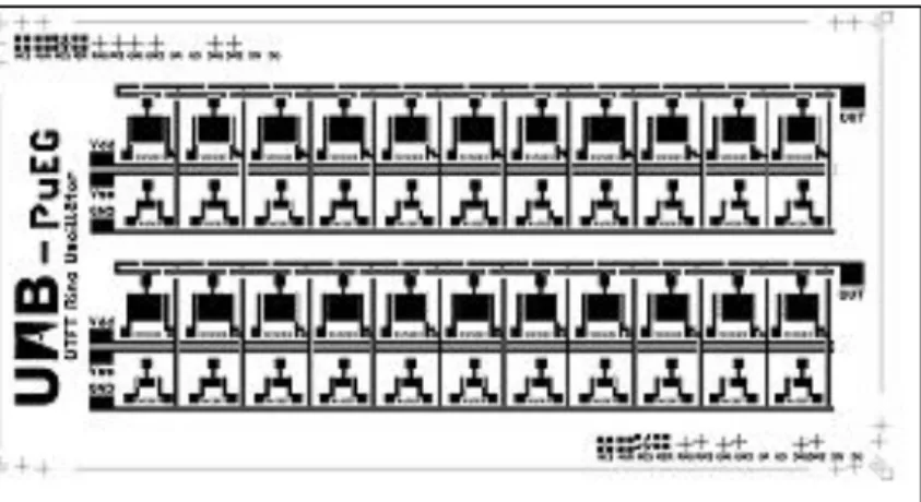
The OTFTs were arranged into the substrates into a configuration where they can easily be wired to make, inverter, oscillator and logic gates circuits. In the RUN2 foil (Fig. 4.2) fabricated at ENEA, the transistors are organized in four rows, where each of them have 11 OTFTs, with two fixed aspect ratios W/L (where W and L are the channel width and length, respectively). The values for the unipolar saturated load transistors are 5000/40 µm and for the driver (input) transistors, W/L are 40000/40 µm.
Fig. 4.2 - Arrays of transistors with two distinct sizes. They were pre-wired to make inverters and oscillators.
The results were obtained connecting two OTFTs (oscillator 2 inverter 10) based on FS 0027 semiconductor (see Fig. 4.3). The used inverter had a driver/load ratio of 8. Several inverter configurations were tested, but the best voltage gain was obtained with the configuration presented in Fig. 4.1 (a).
The driver and load OTFT I-V characteristic curves are presented in Fig. 4.4, and the transfer curves measured in linear region (𝑉!" = −1𝑉) can be seen in Fig. 4.5.
Fig. 4.3 – Optical microscope image. (a) Driver OTFT; (b) Load OTFT
Fig. 4.4 – Output characteristics of the OTFT, (a) large area; (b) small area. The ratio between OTFTs areas is 8.
(a)
(b)
The inverter circuit was operated under relatively low voltages (𝑉!"= 0 − 7 𝑉, 𝑉!! = −15𝑉) in a dark chamber at ambient temperature. The input ramp was
generated using Keithley 487 voltage source. The output voltage values were read by Keithley 2182 Nanovoltmeter.
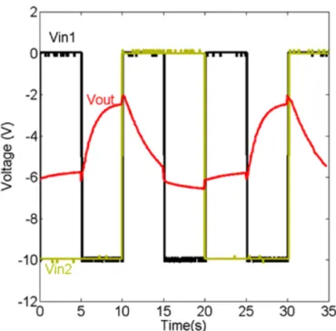
Fig. 4.6 shows the transfer curve of the inverter made using the TFTs on Fig. 4.4 and Fig. 4.5. A full hysteresis loop, when 𝑉!" was cycled in the range [0; -7] V. As the driver TFT moves into accumulation, its resistance decreases and 𝑉!"# moves from a high voltage towards a value limited by the minimum resistance of the driver TFT. The maximum value of output voltage is determined by the resistance of the load TFT, which increases with time due to gate-bias stress.
Fig. 4.6 – Output transfer curve of an inverter circuit and voltage gain.
The increase of load OTFT resistance, that represents the effect of gate-bias stress and lowers gain value, is illustrated in the Fig. 4.7 and Fig. 4.8, which represent the response of application of 3 consecutive input ramps to the inverter.
Fig. 4.7 – Time dependence of 𝑉!"#.
Fig. 4.8 – 𝑉!"# vs 𝑉!" and gain Av, (a) forward path voltage scans and (b) return path voltage scans.
Several consecutive inverter transfer functions are presented in Fig. 4.7 The amplitude of the gain decreases with time from value of 2 to 1.5 in forward path voltage scans (Fig. 4.8 (a)). In the return path, presented in Fig. 4.8 (b), the decrease of gain is
4.3.2 FS0096 INVERTER
OTFTs fabricated in RUN4 were made at TUC installations. In this run, the aspect ratio W/L of transistors was varied, providing four different types of driver/load ratios (8, 10, 12, 16). See Fig. 4.9. Furthermore the semiconductor used is the FS 0096.
Fig. 4.9 - Design with arrays of individual OTFTs with different W/L ratios.
The I-V characteristic of the selected OTFTs, are shown in Fig. 4.10. The ratio between areas is 12.
Fig. 4.10 - Output characteristics of the OTFT, (a) large area and (b) small area OTFT. The ratio between OTFTs areas is 12.
Fig. 4.11 compares the transfer curves measured in the linear region (𝑉!" = −1𝑉). The threshold voltage (𝑉!!) is approximately -2 V for both transistors.
Fig. 4.11 - Comparison between the transfer curves measured in the linear region (𝑉!" = −1𝑉). The
dashed red line is a guide to the yea to estimate the threshold voltage.
The static transfer characteristic of the inverter is shown in Fig. 4.12. The output voltage swing is 10 V with VDD = −20 V. The gain is close to 2.8. High and low noise
margins are respectively NMH =4.5 V and NML=1.8 V.
Fig. 4.12 - Inverter transfer characteristics (black solid line) and gain (red line), 𝑉!!= −20 𝑉 and
𝑉!"= [0; −10]V with a tamp speed of 0.1V/s. The drive/load ratio is 12.
The inverter transfer characteristic do not change with time when driven by a periodic waveform. This confirms that the threshold voltages of both TFTs (driver and load) are relatively stable. This stability is confirmed when the inverter transient
Fig. 4.13 - Inverter response to an input square wave (𝑉!!= −10 𝑉).
The application of successive square waves to the inverters shows that there is a small hysteresis effect. The inverter gain is smaller when it switches between low (-1.7V) and high (-11.5V) state. The process repeats periodically and generates a slightly asymmetric waveform as shown in Fig. 4.14.
Fig. 4.14 - Transient response of the inverter (𝑉!!= −20 𝑉).
This asymmetry is caused by the different switching process because of the inner nature of the pseudo-pMOS circuit, the rising transitions of the output voltage (from ‘0’ to ‘1’) will be much faster that falling transitions (from ‘1’ to ‘0’). This behaviour is due
to the fact that load OTFTs (discharging path) are worse conductors than drive transistors (charging path). The slow time can be comparable with the time length used to record the inverter transfer function. A voltage ramp with speed of 0.1V/s was used, therefore, it only takes 20 seconds to complete a voltage ramp loop [0; -20] V.
The circuit performance is not affect by threshold voltages instabilities (gate-bias stress). Thus in spite the OTFTs used to make these circuits are not encapsulated and been stored in ambient atmosphere laboratory for several months, these findings show that all-inkjet printed OTFTs are robust enough to make circuits.
4.3.3 NAND LOGIC GATE
In order to implement a NAND logic gate, it is necessary to add another OTFT to the inverter circuit (Fig. 4.1 (a)), which will create a possibility of another input. The used circuit and the truth table are presented below.
Fig. 4.15 - (a) NAND gate truth table, (b) NAND gate circuit.
Another OTFT was added to the previous inverter circuit and NAND logic gate was implemented.
The measured response of the NAND gate to square wave input signals 𝑉!"! and 𝑉!"! is shown in Fig. 4.16. As expected, 𝑉!"# follows the truth table for a NAND gate
(figure 4.15.(a)), i.e., remains high (−6 V) except when both inputs are high (−10 V).
NAND Gate VIN1 VIN2 VOUT
0 0 1
0 1 1
1 0 1
1 1 0
Fig. 4.16 - Response of NAND logic circuit, input square wave frequencies are 0.1Hz ( 𝑉!"!) and 0.2 Hz
(𝑉!"!).
4.4 CONCLUSIONS
Inverter circuit and a NAND logic gate were fabricated. Two different runs were used. The maximum gain reached is -3. This is enough to make oscillators. Our findings show that higher gains are possible if the voltage range is extended. However this is not possible in our laboratory due to limitations of the instrument input impedance.
Comparing inverters made with different semiconductors, we found that the inverters using the FS0027 semiconductor show a relatively higher voltage gain degradation under continuous operation. Inverters using the FS0096 are relatively more stable. The reason may lay in slightly different processing methods because they were produced in different laboratories. The major limitation of the circuits is their dynamic response. They can only operate below 1 Hz. We believe this is due to a very large parasitic capacitance between the gate and source and drain terminals.
Chapter 5
PARAMETER VARIABILITY ON ALL-INKJET PRINTED
ORGANIC TFTS
In this chapter, the variability observed in the transistor parameters, such as mobility, threshold voltage and on/off ratio are discussed. Intrinsic sources of variation caused by materials, processing, and handling, variations caused by a bad analysis of the data and finally variability caused by bad transistor design are also analysed and discussed. As a result of this study, the transistor layout was optimized to minimize parasitic effects such as lateral conduction and fringing. It is shown that by using a new pattern design the variability in mobility is minimized.
5.1 INTRODUCTION
Process variations present during transistor fabrication lead to a certain variability on the resulting transistor parameters. Variations between OTFTs had been a well-known problem, more acute than in silicon-based technologies by an inherently much higher parameter spread. Reasons for that, include, irregular morphology of the semiconductor, difficulty in controlling the precise dimensions of OTFTs, mobile trapped charges in the dielectric, uneven material deposition, roughness of the semiconductor-gate dielectric interface which leads to mobility variations between the different transistors.
The large transistor variability poses a serious challenge to the cost-effective utilization of organic analog circuits. Meeting this challenge requires comprehensive and efficient approaches for variability characterization and minimization. Accurate and efficient characterization of the different types of variation requires a large number of measurements on a variety of devices, layout styles, and environments. Data on transistor variability was previously reported by the Bao group [37]. Wei Xiong concluded that the variability observed prohibits the use of their OFETs in
considerable parameter variations have been reported for organic thin-film transistors [39,40,41,42,43,44,45]. These variations find their origin in the organic materials employed and the rather immature printing, technology. They have an impact on one or more parameters of the saturation current equation of thin-film transistors (Eq. (5.1)).
𝐼!"(!"#) =1 2𝜇 𝜖!𝜖! 𝑑 𝑊 𝐿 𝑉!"− 𝑉!! ! (5.1)
where VTh, W, L, µ, εr and εo and d have their usual meaning.
Interesting, not all parameters affect the transistor current on the same way. Variations in the threshold voltage VTh affect the saturation current of the transistor quadratically, while variations in µ, W, L, and d, influence the saturation current only linearly.
This chapter covers a study of parameter variability in all-inkjet printed transistors. It is organized in the following way; first look is based on how the transistor parameters depend on the printed active area. Next, it is shown that parameter extraction can be wrong, if the date is not proper corrected for parasitic off-state current. The strong dependence of the parameters on the active area indicated that the transistor design used was affected by lateral conduction. A new transistor layout was tested showing that the variability can be minimized.
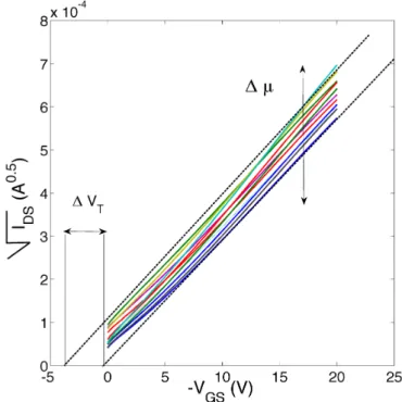
5.2 RESULTS
Studies of variability require a large amount of TFTs. This study made use of 4 foils with TFTs as show in Fig. 5.1. Each foil had 44 TFTs. Two different sizes were available. Large area TFTs have L= 40 µm and W=4 cm. Small area TFTs have L= 40
µm and W=0.5 cm. Two types of organic semiconductors were used, the FS0027 and the FS0096. Not all the TFTs were working. The yield of working TFTs varies from 90% to 27% depending on the foil.
![Fig. 3.2 - Different types of small molecules, typically processed by sublimation [25]](https://thumb-eu.123doks.com/thumbv2/123dok_br/18605096.909566/26.892.239.688.423.679/fig-different-types-small-molecules-typically-processed-sublimation.webp)