Genera
l
ized Chebyshev-
l
ike Approximation
for Low-pass Fi
l
ter
Hisham L. Swady Dept. of Electrical Engineering .
University of Basrah Basrah, Iraq
Email:[email protected]
Abstract—Analog filters constitute indispensible component of analog circuits and still playing an important part in interface with analog real world. realizing filters with odd order is preferred because of its time response . Therefore, this paper is conducted to introduce a new generalized Chebyshev – like approximation for analog filters. The analyses presented to realize the filters with odd order. This proposed novel approach offer good results in terms of flat delay and time domain response. Also, the achieved results are validated by comparison to normal Chebyshev filter via investigation several examples.
I. INTRODUCTION
The analog filter is a linear system that has an input and output signal. This main function of this system is to change the frequency response characteristics of the input signal as it moves through the filter [1]. There are many applications for analog filters, like, amplifiers, voltage controlled oscillator, converters, and sensors etc.. Also, the analog filter is the first step required to build the digital infinite impulse response (IIR) filters by using bilinear transformation or the impulse response[1-3]. The main step for designing all types of analog filters should start with present a normalized platform. Then, the designer should be able to realize the achieved platform with the required scale. The standard normalization located within the range of 0~1 and stopband located in [ws,+∞] [4, 5].
A considered research papers have been conducted to address several efficient optimization techniques [6 - 8]. The exits methods based on utilizing analog platform to be used in realizing the digital filters, or employing some digital filters platform for realizing. So, to achieve improvement for both
types of filters this paper has been conducted to present the required steps for designing analog filters which can be based in building its counterpart of filters- digital filters. This work presents a novel general approach for analog filter designing for Chebyshev-like approximation with odd order. Chebyshev-like filters differs from classical Chebyshev ones in the ripple factor, ε, which is not equal amplitudes with classical one.
II. THE PROPOSED APPROXIMATION
Consider the following general magnitude squared function of a low- pass filter of order N = 2n+ 1[9]:
| ( )| = ( ) ..(1)
Where
ε2= δp-2-1; ..(2)
δp is the minimum value of | ( )|in the passband 0 ≤w≤ 1. The classical approach to obtain a low-pass characteristic is based on searching for a function similar to Eq. 1 and satisfy the following conditions [9]:
( ) ≪ 1 0<<w<<wp
( ) ≫ 1 w>ws
Our approach depends on choosing δp ≤| ( )|≤1 in the passband. After several manipulations the formula is obtained:
max [ ( )] ≤1 ..(3) For a special case with choosing p(w2) = ( )equation 1 becomes identical to the magnitude squared function of the Chebyshev filter[10] as:
Proc. 1st International Conf. Energy, Power and Control Basrah University, Basrah, Iraq 30 Nov. to 2 Dec. 2010
5
Iraq J. Electrical and Electronic Engineering ﺔﻴﻧﻭﺮﺘﻜﻟﻻﺍﻭﺔﻴﺋﺎﺑﺮﻬﻜﻟﺍﺔﺳﺪﻨﻬﻠﻟﺔﻴﻗﺍﺮﻌﻟﺍﺔﻠﺠﻤﻟﺍ
| ( )| =
( )
The value ofnis determined from the stop satisfy:
| ( )| ≤ , ≥
Wherewsandδsdenote the prescribed stop
and the stopband tolerance, respectively. Eq.5 can be transformed into the follow analytical manipulation which results:
P(w2) ≥
Numerical techniques should be used to ev 6 to calculate the filter parameters after pro achieved.
III. VALIDATE THE PROPOSE
To validate the proposed appr be pointed as a first step. Rf. following rational function:
P(w2) = w2∏
This equation will be based in the the design procedure as follows: Given the design specification allowable passband ripple and ma stopband ripple. The Chebyshev filer n can be found as:
Step 1. Maximize Eq. 3 for
Step 2. Substituting the r for gettingws.
Step 3. The pole locations will be obtained by using th
∏ ( − ) = ± ∏ (1 −
IV. DESIGN EX
Let us consider the following d illustrating the proposed scheme. Example 1:
Forn=1, and N = 3, with Eq. 3, the max
..(4)
pband requirement that
..(5) pband edge frequency
wing inequality by an
..(6)
valuate equations 3 and oper choice forp(w2)is
ED SCHEME
oach p(w2) should [11] offered the
..(7)
e prototype. Thus,
ns: maximally ximally allowable like filter of odd
calculatingwi.
esults into Eq. 6
of the new filter his equation[11]:
)/ ..(8)
XAMPLES
design examples for
ximum value of
[ ( − ) ]
givesw = 0.866 w1, then the
2[ − (0.866)]( + 1.7)
Thus,w1≤ 0.866should satis
Thus, Eq.(6) be as :
− − (1 − ) ≥
Then the optimum solution o
ws=3.2and the pole locatio
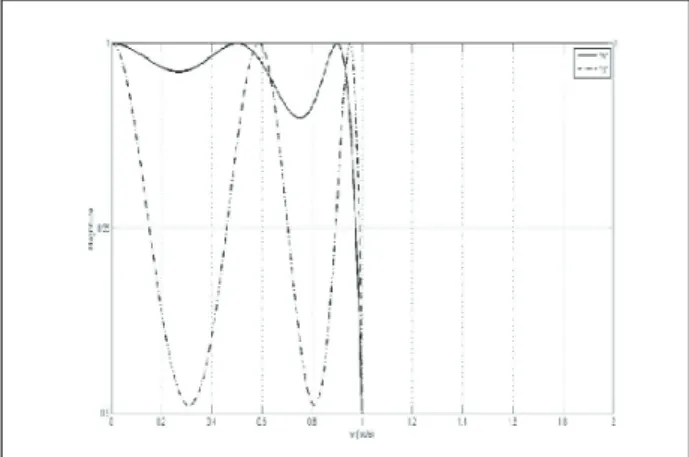
and -0.333 j0.986 for δp =0 The magnitude response of Chebyshev-like are shown i performance of the propo Chebyshev filters under (δp=0.894). It's clear that th has non- equal ripple facto flatness than Chebyshev Furthermore, the improveme can be observed.
Similar procedure is applied results are shown in Fig.3. T is illustrated for range of fre equal and there is an imp response as shown in Fig.4.
Fig.1: Passband performance of
the Chebyshev filters ("B
..(9) inequality of Equ. 3 becomes:
≤ 0 ..(10)
sfy inequality in eq.10 .
≥ 0 ..(11)
of this condition isw1=0.8and
ns of the new filter are -0.665 0.894.
f both of the Chebyshev and in Fig.1. Fig.1 shows passband sed design and the classical r the same specifications he new proposed approximation or in the passband and more filter as shown in Fig.2. ent in the time domain response
d also, for δp =0.891 and the The passband ripple factor and equencies, the ripple also is not provement in flatness of the
the proposed design filter ("A") and
") for δp=0.894, 3 rd order.
6
Iraq J. Electrical and Electronic Engineering ﺔﻴﻧﻭﺮﺘﻜﻟﻻﺍﻭﺔﻴﺋﺎﺑﺮﻬﻜﻟﺍﺔﺳﺪﻨﻬﻠﻟﺔﻴﻗﺍﺮﻌﻟﺍﺔﻠﺠﻤﻟﺍ
Fig. (2) Passband details comparison between ("A")and the Chebyshev filters("B") for δp=0
Fig. (3) Passband performance of the propose and the classical Chebyshev filters ("B order.
Fig. (4) Passband details comparison betwe design ("A")and the Chebyshev filte
order.
proposed design filter .894, 3 rd order.
ed filter ("A") B") δp=0.891, 3rd
een the proposed filter ers("B") for δp=0.891, 3 rd.
Example 2:
For n=2, N=5 used with should be maximize: ..(12)
With utilizing numerical
w1=0.5andw2=0.9 are obtain
Then, the pole locations of th -0.1449±j1.0056 and -0.407± The magnitude response of th
Fig. 5.
The higher order filter des lower ripple magnitude than filter. But this ripple is incre for the high order filters. Thi 5 and 6. Fifth order is also the obtained results are show ripple factor gained clear classical one.
Fig.5: Passband performance o and the Chebyshev filte
eq.3, the following equation
[ ( − ) ( − ) ]
techniques to evaluate wi's.
ned.
he new filter are:-0.5143, ±j0.6076 for δp =0.894.
he two filters are shown in
sign with the new filter offer n that with classical Chebyshev ased as w increases from 0 to 1 is can be shown clearly in Figs. considered for δp =0.891and wn in Figs.7 and 8. It show that improvement compare to the
of the proposed design filter ("A") ers("B"), for δp=0.894, 5th order.
7
Iraq J. Electrical and Electronic Engineering ﺔﻴﻧﻭﺮﺘﻜﻟﻻﺍﻭﺔﻴﺋﺎﺑﺮﻬﻜﻟﺍﺔﺳﺪﻨﻬﻠﻟﺔﻴﻗﺍﺮﻌﻟﺍﺔﻠﺠﻤﻟﺍ
Fig.6 : Passband details comparison between filter ("A")and the Chebyshev filters("B") fo
Fig. 7: Passband performance of the proposed the Chebyshev filters("B") for δp=0.8
Fig. 8: Passband details comparison between filter ("A") and the Chebyshev filters("B") fo
n the proposed design or δp=0.894, 5th order.
d design filter ("A") and 891, 5th order.
n the proposed design or δp=0.891, 5th order.
V. CON
In this paper, we have
Chebyshev-like approxim
design. The approach for
is compared with those
filter. The obtained resu
designed filter gives low
poles with a considerab
filter passband response.
VI. REF [1] H. K. Kim, “The effects having equal ripples in the Syst., Vol. 39, pp. 305-309, [2] F.F. Kuo, Network Analy
Wiley, 1977.
[3] U.Tietzem C.Shank, E.G Circuits. Berlin: Springer, 2 [4] A. Antniou, Digital signal p
Hill, 2006.
[5] S. Winder, Analog and Dig 2002.
[6] N. T. Hoang, H.D. Tuan, T Optimized Analog Filter D Semidefinite Programming" Vol. 57, No. 3, March 2009. [7] T. Iwasaki and S. Hara, “G
frequency domain inequ IEEE Trans. Autom. Contro 2005.
[8] N. T. Hoang, H.D. Tuan, T Optimized Analog Flat Fil Processing, Vol. 57, No. 3, M [9] K.Su, Analog Filte
publishers,2002.
[10] M. Weeks, Digital Signal Wavelets. Infinity Science p [11] S.C. Dutta Roy, "A New Approximation" , Spring LLC2010, Circuit Syst. Sig
NCLUSION
e addressed a generalized
mation for low-pass filter
r one approximation method
of the classical Chebyshev
ults show that the proposed
wer Q values of complex
ble value of flatness of the
FERENCES
of lower Q values on the filters passband” , IEEE Trans. Circuits 1992.
ysis and Synthesis. New York,
Gamm, Handbook of Electronic 2008.
processing. New York:
McGraw-gital Filter Design, 2nd , Newnes,
T. Q. Nguyen, and H. G. Hoang," Designs With Flat responses by ", IEEE Trans. Signal Processing, .
Generalized KYP lemma: Unified ualities with design applications,” ol, vol. 50, no. 1, pp. 41–59, Jan.
T. Q. Nguyen, and H. G. Hoang," lter Design", IEEE Trans. Signal March 2009.
ers, 2nd. Kluwer Academic
Processing using MATLAB and press,2007.
w Chebyshev-like Low-pass Filter ger Science+ Business Media, gnal process Vol. 29: pp 629-636.
8
Iraq J. Electrical and Electronic Engineering ﺔﻴﻧﻭﺮﺘﻜﻟﻻﺍﻭﺔﻴﺋﺎﺑﺮﻬﻜﻟﺍﺔﺳﺪﻨﻬﻠﻟﺔﻴﻗﺍﺮﻌﻟﺍﺔﻠﺠﻤﻟﺍ