Brazilian Journal of Physics, vol. 39, no. 3, September, 2009 543
Annealing time effect on the properties of
CuInSe
2grown by electrodeposition using two
electrodes system
A. Bouraiou∗
Laboratoire des Couches Minces et Interfaces, D´epartement de Physique, Universit´e Mentouri-Constantine, Constantine 25000, Algeria and
Institut des Sciences et Technologies, Universit´e Ziane Achour Djelfa 17000, Algeria
M.S. Aida, A. Mosbah, and N. Attaf
Laboratoire des Couches Minces et Interfaces, D´epartement de Physique, Universit´e Mentouri-Constantine, Constantine 25000, Algeria
(Received on 18 March, 2009)
In this paper, we report the effect of annealing time on the properties of copper indium diselenideCuInSe2
films. TheCuInSe2thin films have been grown at room temperature by electrochemical deposition technique
using two electrodes system. The as deposited films were annealed under argon atmosphere at 300oCduring
15, 30, 45 and 60 min. The structural and morphological properties of the resulting films were characterized respectively by means of x-ray diffraction (XRD) and scanning electron microscopy (SEM). The optical band gap was estimated from transmittance measurements. We have found, that after annealing, all films present
CuInSe2in its chalcopyrite structure and with preferred orientation along<112>direction. The film annealed
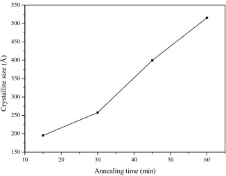
during 45 min exhibits better crystallinity and excellent optical properties. The SEM pictures show that the elaborated films have a uniform surface morphology with a homogeneity distribution of crystallites, the grain became higher in size with prolongation of annealing time; it lays in the range of 195 to 515 ˚A.
Keywords: thin films,CuInSe2, electrodeposition, annealing time
1. INTRODUCTION
Copper indium diselenide thin filmsCuInSe2(CIS)
pos-sess direct band gap material, high optical absorption coeffi-cient, reasonable work function, high long-term stability and largest efficiency in photovoltaic applications (it achieved an efficiency of 19 %) [1]. The homojunction and heterojunc-tion solar cells can be prepared from this semiconductor [2]. Despite of its weak contribution to the photovoltaic market (1 %) [3], all these characteristics make theCuInSe2one of the
most promising materials for second-generation solar cells [4,5].
The efficiency of solar cells based onCuInSe2films is
crit-ically influenced by several parameters such as the elabo-ration technique, the experimental parameters, the preferred orientation ofCuInSe2growth layer and substrate properties
[6], etc.
CuInSe2 thin films can be prepared by several methods.
The electrodeposition method is probably the most appropri-ate and promising. This is due to its low cost, easiness, high efficiency, non vacuum and stability of the product [7,8].
In the literature there are numerous reports about the film growth by electrodeposition technique using a three elec-trodes system (cathode, electrode, reference electrode) [9-13]. The reference electrode has always been used to mea-sure the cathode voltage with respect to it. On the other hand, it is an external impurity source and hence could poison the bath, and drastically reduce the efficiency of solar cells [14]. In our knowledge, Dhamardasaet al. [14] are the only ones who used a system with two electrodes for the deposition of CuInSe2material.
In our work, we have grownCuInSe2 by using the
elec-∗Electronic address:[email protected]
trochemical deposition technique using two electrodes sys-tem, and cconsidering its properties such as excellent elec-trical conduction, excellent optical transmission in the visi-ble range (around 80 %), very significant reflectance in the infrared range, excellent adherence with the glass substrate [15], the indium tin oxide (ITO) coated glass is used as the substrate on which we deposit the films. The structural, mor-phological and optical properties of the resulting films were studied as a function of the annealing time.
2. EXPERIMENTAL
CuInSe2thin films were electrochemically deposited
us-ing two electrodes cell configurations. The instrumentation and the deposition method were the same as described in a previous work [6]. The ITO coated glass substrate is used as the working electrode (cathode). A platinum plate was used as the counter electrode (anode). A Voltammograms Multi-Potentiostat was used to control the electrodeposition process and to monitor the current and voltage profiles.
The electrolyte bath used for the films elaboration con-sisted of 10 mM copper chloride (CuCl2), 40 mM indium
chloride (InCl3) and 20 mM selenium oxide (SeO2)
dis-solved in de-ionized water. The films were deposited at room temperature, without agitation, using a deposition potential of−7V, and then the as deposited films were annealed un-der argon atmosphere at 300oCduring various heating times: 15, 30, 45 and 60 min.
The x-ray diffraction was accomplished by a Philips PZ 3710 x-ray diffractometer using monochromaticCuKα1
544 A. Bouraiou et al.
card was done for the identification of the observed peaks. The crystallites sizeDis calculated from the Halder and Wagner approximation [16,17].
The surface morphology of the films was observed by sec-ondary scanning electron microscope ZEISS-SUPRA 55VP type. Spectral transmittance was recorded using Shimadzu mode UV-3101 PC spectrophotometer. The measurements were carried out in wavelengths within the range of 400-1800 nm with 2 nm steps.
The films thicknesstwas estimated theoretically using the following formula [18,19]:
t= 1
nFA isM
ρ
(1)
Here,nis the number of electrons transferred, it was taken as 13, F= 96500 C is Faraday’s number, A is the elec-trode area,iis the applied current, sis the deposition time, M =336.28g mol−1is theCuInSe2 molecular weight and
ρ=5.77g cm−3is the density ofCuInSe2material [20].
3. RESULTS AND DISCUSSION
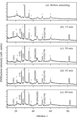
Figure 1 (a-e) shows the x-ray diffraction patterns of the elaborated samples respectively for the as deposited film and for annealing films at 300oCduring 15, 30, 45 and 60 min.
The peaks noted1 in Fig. 1 and located at 2θ≈21.300,
30.300, 35.260, 37.420, 50.660and 60.300correspond to the
most intense peaks of ITO phase. Fig. 1(a) shows only the ITO phase, which reveals the amorphous structure of the de-posited layer.
As can be seen in Fig. 1, after annealing, all the spec-tra appear the peaks located at 2θ≈17.100, 26.660, 27.660,
44.300, 52.500and 81.380. These last peaks correspond to
the most intense peaks given in the JCPDS card (File N◦: 40-1487) forCuInSe2, they are corresponding respectively
to the (101), (112), (103), (204)/(220), (116)/(312) and (424) planes [21]. On the other hand, the calculation of the pref-erential orientation degree in the films [6,22] shows the high degree of preferred orientation towards the<112>direction
and the film annealed during 45 min presents the higher in-tensity ratio. This confirmed that all annealed films present a chalcopyrite phase ofCuInSe2with a tetragonal structure
and with<112>as preferred orientation.
The full width at half maximum FWHM and d-spacing of the(112) peak, respectively noted βexp(112) andd112,
ver-sus the annealing time are shown in Fig. 2. The inter-planar spacingd112was calculated using Bragg’s relation [23], the
obtained values belong are in agreement with the standard JCPDS card [20].
As can be seen from the Fig. 2, theβexp(112)follows the opposite trend ofd112. Thed112of the film annealed during
45 min is the highest one and it is closest to that given in the JCPDS card. However, the evolution of theβexp(112)is a decreasing function of annealing time, and the (112) peak becomes narrower and more intense for the film annealed during 45 min, so this film exhibits better crystallinity. This is due to the reduction of the structure defects and internal stresses which result from the rearrangement of the atoms in the structure.
20 40 60 80
(1 03 ) (10 1) 1 1 1 1 1 1 1 (1 12) 4(deg.) (204 )/(2 20) (10 3) (10 1) 1 1 1 1 (2 04) /(22 0) (112)
(d): 45 min
(e): 60 min 1 (101 ) (31 2)/ (116 ) 1 1 1 1 1 (20 4)/(2 20 ) (11 2) (1 03 ) (31 2)/(1 16 ) 1 1 1 1 1 1 1 1 1 1 1 (31 2)/(1 16 ) (204 )/(2 20) (1 12)
(c): 30 min (b): 15 min
(3 12)/ (11 6 ) 1 (42 4) (4 24 ) (4 24) (424 ) (1 03 ) (10 1) 1 D if fra ct ion inte nsity (a rb units )
(a): Before annealing
FIG. 1: XRD patterns ofCuInSe2as depoisted on ITO coated glass
substrate by electrodeposition technique after annealing at 300oC for different annealing times:(a): as deposited film, (b): 15 min, (c): 30 min, (d): 45 min and (e): 60 min. The peaks noted1correspond to the ITO phase.
In order to separate the microstrainsεand crystallites size Deffect on the line broadening, we used the approximation introduced by Halder and Wagner [16,17]:
β∗ stru d∗ 2 = 1 D β∗ stru
(d∗)2+
ε 2
2
(2)
Whered∗is the inter-planar spacing considered in the recip-rocal space andβ∗struis given by the following relation:
β∗stru=
βexpcosθ2−(βinstcosθ)2 λ βexpcosθ
(3)
Whereβexp andβinst are respectively the experimental and instrumental widths calculated from the diffraction spectra of the standard sample andλis the radiation wavelength of the x-ray source.
After having calculatedβ∗stru andd∗for the most intense peaks, we plot the β∗stru
d∗
2
evolutions versus β∗stru
Brazilian Journal of Physics, vol. 39, no. 3, September, 2009 545
10 20 30 40 50 60
3.320 3.325 3.330 3.335 3.340 3.345
d112
Eexp(112)
Annealing time (min)
d 112
(Å
)
0.30 0.33 0.36 0.39 0.42 0.45 0.48 0.51
E
ex
p (112) (ra
d)
FIG. 2:βexp and d-spacing of the (112) peak as a function of an-nealing time.
10 20 30 40 50 60
150 200 250 300 350 400 450 500 550
Cry
stal
lit
e size
(Å)
Annealing time (min)
FIG. 3: Crystallite size as a function of annealing time.
from this figure, the crystallite size is a linearly increasing function of annealing time; it lays in the range of 195 to 515
˚ A.
The SEM micrographs of the films annealed during 15, 30, 45 and 60 min are shown respectively in Figs. 4(a-d). The film annealed during 15 min (Fig. 4(a)), shows a smooth, ho-mogenous and small grain size. The film annealed during 30 min (Fig. 4(b)) presents a uniform surface morphology but less dense crystal structure with the appearance of a greater grain size of about 0.5µm at the surface. The films annealed during 45 and 60 min (Figs 4(c, d)) are compact and show a good uniform surface morphology with a more dense homo-geneity distribution of grains.
In order to supplement the previous analysis, we corre-lated the structural and morphological characterizations with optical measurements. For this, we must calculate the thick-ness of the as deposited films from the equation (1). We have obtained 0.9µm.
It is well known thatCuInSe2is a direct gap
semiconduc-tor, so the absorption coefficient in the region of strong
ab-(a)
25000× 2 Pm
(b)
25000× 2 Pm
(c)
25000× 2 Pm
(
d)25000× 2 Pm
546 A. Bouraiou et al.
sorption obeys the following equation [24]:
α= C
hν(hν−Eg)
1
2 (4)
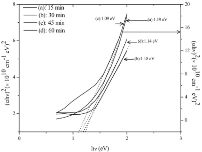
Where h is the Planck constant, ν is the radiation fre-quency,Egis the band gap energy andCis a constant. TheEg value of the different thin films were evaluated from the plot of squares of optical absorption coefficient (αhν)2as
func-tion of the photon energy (hν) (Fig. 5 (a-d)). The obtained results are displayed in Fig. 5.
0 1 2 3
2 4 6 8
(a): 15 min (b): 30 min (c): 45 min (d): 60 min
hQ(eV)
(
D
h
Q
)2
(
u
10
10 cm -1 eV)
2 (d):1.14 eV
(c):1.09 eV
(b):1.18 eV (a):1.19 eV
0 4 8 12 16 20
(
D
h
Q
) 2
(
u
10
10
cm
-1
eV
) 2
FIG. 5: Variation of(αhν)2as a function of radiation energyhν of elaborated thin films after annealing at 300oCfor different an-nealing times: (a): 15 min, (b): 30 min, (c): 45 min and (d): 60 min.
The estimated band gap was found relatively higher for
the films annealed during 15 and 30 min. However, theEg of the film annealed during 45 min is estimated to 1.09 eV; it is lower than that of the 15, 30 and 60 min. As announced above, this decreasing can be explained by the rearrangement of the atoms in the structure and annealing of some defects with annealing time. These defects appear as deep and shal-low level in the band gap of the elaborated semiconductors material. We note also that, theEgof the last film is less than the optimum value of the terrestrial solar spectrum and it is in good agreement with the results published in the literature [25,26]. The study of the electrical properties of these films is in progress.
The films characterization suggests that the film annealed during 45 min is the optimal one forCuInSe2 production
which used may be as an absorber layer in the fabrication of thin film solar cells.
4. CONCLUSION
The CuInSe2 films were successfully deposited on ITO
coated glass substrate using electrochemical technique. The structural, morphological and optical properties ofCuInSe2
films were studied in terms of annealing time. It was found that the annealing time plays an important role in the evolu-tion ofCuInSe2properties. Before annealing, the XRD
spec-tra only shows the ITO phase peaks and after annealing at 300oC, all the resulting films show the tetragonal chalcopy-riteCuInSe2. The average grain size of the films increases
linearly with annealing time. The film annealed during 45 min exhibits better crystallinity, higher intensity ratio and a good optical properties, it can be used as an absorber layer in the fabrication of thin film solar cells.
[1] F. Kang, J. Ao, G. Sun, Q. He, Y. Sun, J. Alloys Compd. (2009), doi:10.1016/j.jallcom.2008.12. 020.
[2] S. Agilan, D. Mangalaraj, Sa.K. Narayandass, G. Mohan Rao, Physica B,365(2005) 93.
[3] F. Abdo, Ph.D. Thesis, Institut national des sciences appliques de Lyon, France (2007).
[4] M. Altosaar, M. Danilson, M. Kauk, J. Krustok, E. Mellikov, J. Raudoja, K. Timmo, T. Varema, Sol. Energy Mater. Sol. Cells,87(2005) 25.
[5] H.T. Shaban, M. Mobarak, M.M. Nassary, Physica B, 389
(2007) 351.
[6] A. Bouraiou, M.S. Aida, E. Tomasella, N. Attaf, J. Mater. Sci.
44(2009) 1241.
[7] M.E. Calixto, P.J. Sebastian, R.N. Bhattacharya, R. Noufi, Sol. Energy Mater. Sol. Cells,59(1999) 75.
[8] D. Lincot, Thin Solid Films,487(2005) 40.
[9] S. Moorthy Babua, A. Ennaoui, M.Ch. Lux-Steiner, J. Cryst. Growth,275(2005) e1241.
[10] S.H. Kang, Y.K. Kim, D.S. Choi, Y.E. Sung, Electrochimica Acta,51(2006) 4433.
[11] L. Zhang, F.D. Jiang, J.Y. Feng, Sol. Energy Mater. Sol. Cells,
80(2003) 483.
[12] A.A.I. Al-Bassam, Physica B,266(1999) 192.
[13] J.L. Xu, X.F. Yao, J.Y. Feng, Sol. Energy Mater. Sol. Cells,73
(2002) 203.
[14] I.M. Dharmadasa, R.P. Burton, M. Simmonds, Sol. Energy Mater. Sol. Cells,90(2006) 2191.
[15] K. Daoudi, Ph.D. Thesis, Univ. Claude Bernard - Lyon 1, France (2003).
[16] N. C. Halder, C. N. J. Wagner, Acta Cryst.20(1966) 312. [17] R.S. Lei, M.P. Wang, M.X. Guo, Z. Li, Q.Y. Dong, Trans.
Nonferrous Met. Soc. China,17(2007) s603.
[18] R. Friedfeld, R.P. Raffaelle, J.G. Mantovani, Sol. Energy Mater. Sol. Cells,58(1999) 375.
[19] M. Faraday, Philos. Trans. R. Soc.124(1834) 77.
[20] R.C. Weast (Ed.), CRC Handbook of Chemistry and Physics, CRC, Boca Raton, FL, 1980.
[21] International Center for Diffraction Data, ICDD, PDF2 database.
[22] J. Muller, J. Nowoczin, H. Schmitt, Thin Solid Films, 496
(2006) 364-370.
[23] B.D. Cullity, Elements of X-Ray Diffraction, Addison-Wesley, Reading, MA, (1972) p.102.
[24] J.C. Berned, L. Assmann, Vacuum,59(2000) 885.
[25] R.P. Raffaelle, H. Forsell, T. Potdevin, R. Friedfeld, J.G. Man-tovani, S.G. Bailey, S.M. Hubbod, E.M. Gordon, A.F. Hepp, Sol. EnergyMater. Sol. Cells,57(1999) 167.