*e-mail: [email protected]
1. Introduction
Tin-doped indium oxide (ITO) ilms with high conductivity and transparency have been extensively served as transparent and conductive electrodes in optoelectronic devices1. There are some techniques to deposit the ITO ilms, such as magnetron sputtering, pulsed laser deposition, electron beam (EB) evaporation, chemical vapor deposition, sol-gel, spray pyrolysis2-7. Among these different methods, the EB evaporation technique is one of the most frequently used methods for producing ITO ilms having better electrical and optical properties, which is easy to be applied to commercial production8. Some investigative works have reported the relationship between the EB evaporation process and the properties of the ITO ilms4,8-12, such as oxygen,
post-annealing, substrate temperature, ingredient ratio. One of the most important applications of the ITO ilms deposited by EB evaporation is served as the p-type electrodes of GaN-based light emitting diodes (LEDs). The utilization of the ITO ilms substituting for metal ilms can enhance the output of light from GaN-based LEDs13,14, which is due to
its low direct current resistivity and high transmittance in the visible light range.
To the best of our knowledge, the high density ITO targets used for magnetron sputtering were served as the raw material of EB evaporation process. However, the ITO tablets designed for the source of EB evaporation were rarely investigated. In general, the low density of ITO tablets with about 62% relative density were designed to resist thermal shock of high energy electron beam. The surface needles or the internal cracks of the low density ITO tablets may be formed during EB evaporation process. Obviously, the
formation of these needles or cracks are likely to change the scattering angel of the oxide vapor during evaporation process. These slight luctuations would deteriorate the structural, electrical and optical properties of the deposited ITO ilms, such as resistivity, transmittance and uniformity. These deteriorated ITO ilms used for GaN-based LEDs would inluence its electrical and optical properties.
In this work, the formation mechanism of the needles and cracks in the low density ITO tablets were investigated, and the corresponding solutions were proposed.
2. Experiments
The conventional ITO tablets were fabricated by using the sintered-ITO powders. The modiied ITO tablets were fabricated by using the nano- and sintered-ITO powders. The sintered-ITO powders were obtained by pressing and sintering the nano-ITO powders at 1200 °C. Then, the nano-and sintered-ITO powders, organic agents and water were grinded, dried and granulated. Finally, the conventional and modiied ITO tablets with dimension of Φ25×10 mm were sintered at 1350 °C under oxygen atmosphere. The ITO tablets were evaporated by electron beam to analyze the needles and cracks.
The microstructure and ingredients of the needles and tablets were analyzed by scanning electron microscope (SEM) using JSM-5610LV (JEOL) and F50 (FEI Inspect). Thermal conductivity was measured by laser lash thermal constant analyzer (TC-7000, ULVAC-RIKO). Three-point bending strength of the ITO tablets were measured by electronic universal testing machine (Shimadzu, AG-X). The optical
Study on Needles and Cracks of Tin-doped Indium Oxide Tablets for
Electron Beam Evaporation Process
Jiwen Xua,b*, Zupei Yangb, Xiaowen Zhanga, Ling Yangc, Huarui Xub, Hua Wanga
aGuangxi Key Laboratory of Information Materials, Guilin University of Electronic Technology,
Guilin 541004, P.R. China
bSchool of Material Science and Engineering, Shaanxi Normal University, Xi’an 710062, P.R. China
cGuangxi Experiment Center of Information Science, Guilin University of Electronic Technology,
Guilin 541004, P.R. China
Received: July 20, 2014; Revised: June 12, 2015
Tin-doped indium oxide (ITO) tablets were used to deposit ITO ilms on p-GaN layer of light-emitting diodes. Needles and cracks in ITO tablets generated during electron beam evaporation process were deeply investigated. The formation of needles is predominantly resulted from the scanning trace, which is controlled by x and y axes scanning singles. The needles can be eliminated by controlling
electron beam scanning trace. The loose microstructure with uniform grains and pores in the ITO tablets results in weak bonding strength, which leads to cracks under the thermal shock of high energy electron beam. A three-dimensional reticulated skeleton structure with strong bonding strength can restrain these cracks.
Xu et al.
520 Materials Research
transmittance in the visible light range was measured by spectrophotometer (V-600, Jasco).
3. Results and Discussion
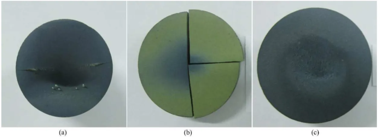
Figure 1 shows the images of surface morphology of the evaporated ITO tablets. As shown in Figure 1a, the protuberances (named needle) erect on the surface of the evaporated conventional ITO tablets. The cracks are also observed and spread out as shown in Figure 1b. Figure 1c shows an integrity appearance of the modiied ITO tablets after EB evaporation. The needles and cracks in the conventional ITO tablets would inluence the divergence angle of oxide vapor and even generate dust in the coating chamber, which forms particle contamination on the ITO ilm surface, and deteriorates the electrical and optical properties of GaN-LEDs.
The thermal conductivity of the conventional and modiied ITO tablets is 7.2 and 8.5 W·m–1K–1, respectively. The conventional and modiied ITO tablets show low thermal conductivity, which indicates that the elimination of cracks is dependent on microstructure rather than the thermal conductivity. Figure 2 shows the SEM images of the conventional ITO tablets. The microstructure indicates that the ITO tablets possesses uniform density at different
positions. The size of grains and pores is uniform, and its distribution is homogeneous. This single coniguration shows loose structure with weak bonding strength. Thermal shock-resistant of this ITO tablets is weak under the bombardment of high energy electron beam during EB evaporation process. Therefore, this homogeneous structure is easily destroyed by thermal shock of EB evaporation or reactive plasma deposition (RPD) process.
Figure 3 shows the SEM images of the modiied ITO tablets. As shown in Figure 3a, the microstructure indicates that the modiied ITO tablets are composed of dense blocky grains (region A) and loose pores (region B). Figure 3b and Figure 3c indicate that the dense blocky regions resemble the dense structure of an high density ITO ceramic target15, a few pores exist in the grain boundaries. Figure 3d and Figure 3e indicate that the loose porous regions is similar with the microstructure of porous ceramic16, a number of pores exist in the grain boundaries. The modiied ITO tablets show heterogeneous structure, which provides a way to enhance the bonding strength.
The microstructure models of the conventional and modiied ITO tablets are demonstrated in Figure 4. The heterogeneous and porous structure can be considered as an effective solution for resisting thermal shock of the ITO
Figure 1. Images of (a) needles, (b) cracks in conventional ITO tablets, and (c) a complete modiied ITO tablet.
tablets when they are heated by high energy electron beam. However, the bonding strength of the single structure is weak, which is easily broken under thermal shock. The structure of the modiied tablets is reticulated with some skeletons. This three-dimensional reticulated skeleton structure simultaneously solves the problems of thermal expansion and bonding strength. The long strip samples were fabricated to measure three-point bending strength and analyze the bonding strength. The bonding strength of the conventional and modiied ITO tablets is about 3.5 MPa and 14.3 MPa, which shows an obvious improvement. Consequently, the cracks in the modiied ITO tablets can be eliminated during the EB evaporation process.
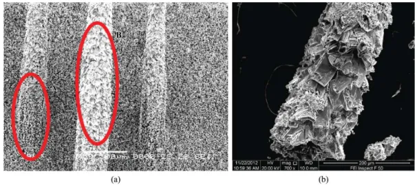
Figure 5 shows the microstructure of the needles. The middle section of the needle (region B) is composed of large blocky ITO grains, which can be clearly observed in Figure 5b and Figure 6. However, the structure of the bottom
section (region A) is consistent with the intrinsic grains of the as-fabricated ITO tablets.
The EDS analysis of the needles, shown in Figure 6, indicates that the blocky needle is composed of indium, tin and silicon. The as-fabricated ITO tablets with a trace of silicon are inevitable, the other impurities are invisible. Therefore, The EDS results indicate that the needles are not caused by impurities. The melted ITO tablet vapor causes abnormal grain growth, which results in blocky needles on the surface.
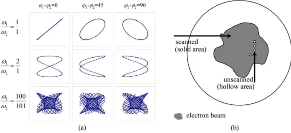
During EB evaporation process, the EB size is about several millimeters. In order to etch the tablet as large as possible, the EB is usually scanned by applying external scan signals at x and y axes. The signal may be sine, triangle
and square waves. The EB scan trace can be described by Lissajous curve. Lissajous curve is the graph of a system of parametric equations17:
Figure 3. SEM images of the modiied ITO tablets: (a) overall view, (b) dense region (region A), (c) magniication of dense region, (d) loose region (region B), (e) magniication of loose region.
Xu et al.
522 Materials Research
1 1
x(t)=A sin(ω + ϕt ) (1)
2 2
y(t) Bsin( t= ω + ϕ ) (2)
Where A and B are the amplitude, ω1 and ω2 are the angular frequency, and φ1 and φ2 are the phase. The appearance of the Lissajous curve is highly sensitive to the frequency ratio of ω1/ω2 and the phase difference of φ1-φ2.
Figure 7a shows nine Lissajous curves, and the more sophisticated curves can be obtained by adjusting the frequency ratio and phase difference. Furthermore, these scan trace curves keep a ixed path and continuously repeat when the scan signals are unchanged. Therefore, the adjustment of the EB size and scan trace is an essential way to resolve the needle problem.
Large size EB and rational frequency ratio can enable the EB to scan the entire surface area of the ITO tablet. However, Figure 5. SEM images of (a) needles and (b) magniication of region B.
the EB size is normally ixed at a value (e.g. 2 mm), which can not be adjusted by operator. Therefore, only frequency ratio can be controlled. If the frequency ratio of ω1/ω2 is inappropriate, some regions of the ITO tablet surface can not be scanned by EB, and these regions can not be gasiied by high energy electron beam. Therefore, these regions contribute to the needles as shown in Figure 7b. It is obvious that the quantity and size of needles are closely related with the EB size and frequency ratio. The proposed frequency ratio should have large simple integer ratio (m/n, m and n is simple integer), such as 30/1, 44/3.
The ITO ilm with 250 nm thickness used for GaN-LED of 455 nm wavelength was deposited onto glass substrate by
using modiied ITO tablet at optimized process parameters. Figure 8 shows the transmittance (including the absorption of glass substrate) of the ITO ilm and the etched patterns of the ITO electrodes. It can be seen that the ITO ilm shows ultrahigh transmittance of about 90% at desired 455 nm, which contributes to increase the output of light at 455 nm. The etched patterns of ITO electrodes indicates that the patterns show sharp edge and have no abnormal spot, crack and etching residue.
4. Conclusions
In this work, the needles and cracks of the conventional ITO tablets used for the EB evaporation process were deeply investigated. The formation of the needles during EB evaporation process is mainly due to the EB size and scan trace which controlled by x and y axes scan signals. The needles problem can be solved by controlling the EB scan trace. The conventional tablets composed of homogenous grains and pores show loose microstructure and easily split under thermal shock of the high energy electron beam. The cracks problem can be solved by constructing a three-dimensional reticulated skeleton structure with blocky and porous regions. The 250 nm thickness ITO ilm shows high transmittance of 90% at 455 nm wavelength of GaN-based LED.
Acknowledgements
This work is jointly supported by the National Science Foundation of China (21176051, 61361004), Guangxi Key Laboratory of Information Materials Foundation (1210908-204-Z, 131024-Z) and Guangxi Experiment Center of Information Science.
Figure 7. (a) Lissajous curves at different frequency ratios and phase differences, and (b) EB scan model.
Figure 8. Transmittance of the ITO ilm and the etched patterns
of the ITO electrodes.
References
1. Lewis BG and Paine DC. Applications and processing of
transparent conducting oxides. MRS Bulletin. 2000; 25(8):22-27. http://dx.doi.org/10.1557/mrs2000.147.
2. Xu J, Yang Z, Zhang X, Wang H and Xu H. Structural, electrical, optical properties and reliability of ultra-thin tin doped indium
oxide films for touch panels. Journal of Materials Science Materials in Electronics. 2014; 25(4):1792-1797. http://dx.doi.
org/10.1007/s10854-014-1800-y.
Xu et al.
524 Materials Research
4. Mohamed HA. Effect of substrate temperature on physical
properties of In2O3:Sn films deposited by e-beam technique.
International Journal of Physical Sciences. 2012; 7(13):2102-2109.
5. Szkutnik PD, Roussel H, Lahootun V, Mescot X, Weiss F and Jiménez C. Study of the functional properties of ITO grown by metalorganic chemical vapor deposition from different indium
and tin precursors. Journal of Alloys and Compounds. 2014; 603:268-273. http://dx.doi.org/10.1016/j.jallcom.2014.03.088.
6. Jafan MM, Zamani-Meymian M, Rahimi R and Rabbani M. Effect of pyrolysis temperature on the electrical, optical, structural, and morphological properties of ITO thin films prepared by
a sol–gel spin coating process. Microelectronic Engineering. 2014; 130:40-45. http://dx.doi.org/10.1016/j.mee.2014.09.009.
7. Marikkannu S, Kashif M, Sethupathy N, Vidhya VS, Piraman S, Ayeshamariam A, et al. Effect of substrate temperature on indium tin oxide (ITO) thin films deposited by jet nebulizer spray pyrolysis and solar cell application. Materials Science in Semiconductor Processing. 2014; 27:562-568. http://dx.doi. org/10.1016/j.mssp.2014.07.036.
8. Cho BR and Park IY. Effect of post-annealing on the formation
of ITO thin films. Journal of the Korean Physical Society. 2008; 53(1):19-22.
9. Yosvichit B, Horprathum M, Eiamchai P, Patthanasetakul V, Samransuksamer B, Chindaudom P, et al. Effect of emitting current ion source on structural, optical and electrical properties of nanostructured ito thin films by ion-beam assisted evaporation.
Advanced Materials Research. 2014; 979:263-266. http://dx.doi.
org/10.4028/www.scientific.net/AMR.979.263.
10. Pokaipisit A, Horprathum M and Limsuwan P. Influence of
annealing temperature on the properties of ITO films prepared
by electron beam evaporation and ion-assisted deposition.
Kasetsart Journal. 2008; 42(5):362-366.
11. Kim K-K, Kim H, Lee S-N and Cho S. Structural, optical, and electrical properties of E-beam and sputter-deposited ITO films for LED applications. Electronic Materials Letters. 2011; 7(2):145-149. http://dx.doi.org/10.1007/s13391-011-0610-0.
12. Yamaguchi M, Ide-Ektessabi A, Nomura H and Yasui N.
Characteristics of indium tin oxide thin films prepared using
electron beam evaporation. Thin Solid Films. 2004; 447-448:115-118. http://dx.doi.org/10.1016/j.tsf.2003.09.033.
13. Chang CS, Chang SJ, Su YK, Kuo CH, Lai WC, Lin YC, et al. High brightness ingan green leds with an ITO on n++-SPS upper contact. IEEE Transactions on Electron Devices. 2003; 50(11):2208-2212. http://dx.doi.org/10.1109/TED.2003.819091.
14. Kuo CH, Chang SJ, Su YK, Chuang RW, Chang CS, Wu LW, et al. Nitride-based near-ultraviolet LEDs with an ITO
transparent contact. Materials Science and Engineering B. 2004; 106(1):69-72. http://dx.doi.org/10.1016/j.mseb.2003.09.018.
15. Zhu G, Yang Z, Zhi L, Yang H, Xu H and Yu A. Preparation and Sintering Behavior of the Tin-Doped Indium Oxide Nanopowders.
Journal of the American Ceramic Society. 2010; 93(9):2511-2514. http://dx.doi.org/10.1111/j.1551-2916.2010.03851.x.
16. Sakka Y, Tang F, Fudouzi H and Uchikoshi T. Fabrication of porous ceramics with controlled pore size by colloidal processing.
Science and Technology of Advanced Materials. 2005; 6(8):915-920. http://dx.doi.org/10.1016/j.stam.2005.07.006.