Study of Short Channel Effects in
n
-FinFET Structure for
Si, GaAs, GaSb and GaN Channel Materials
Tawseef A. Bhat
1,*, M. Mustafa
2, M.R. Beigh
21
Department of Electronics, Govt. Degree College (Boys), Anantnag-192101 India
2
Department of Electronics & Instrumentation Technology, University of Kashmir, Srinagar-190006 India
(Received 10 February 2015; published online 20 October 2015)
In this paper a study of various short channel effects (SCE’s) of double gate n-FinFET structure as a function of scaling parameters for Si, GaAs, GaSb and GaN channel materials has been evaluated and pre-sented. The simulation results presented are based on the self consistent solution of Poisson and drift-diffusion equations. In the model the carrier velocity is assumed to be saturated in the channel for all the materials. Gate length (Lg) and channel width (Wch) dependence of the various short channel effects viz.,
Drain Induced Barrier Lowering (DIBL), Subthreshold Slope (SS) and threshold voltage roll-off of these devices using the said materials have been studied and presented.
Keywords: SCE, DIBL, SS, Threshold voltage, FinFET, ITRS.
PACS numbers: 85.30.De, 85.30.Tv
*
[email protected]
1.
INTRODUCTION
The intensive downscaling of CMOS has been major
driving force behind the aggressive increase in
transis-tor density and performance, leading to more chip
func-tionality at higher speeds. As the device dimensions are
scaled towards the nanometre regime, conventional
single gate MOSFETs experience various short channel
effects (SCE’s) that
deteriorate the drive current and
lead to off-state leakages. To address such scaling down
issues, alternate multiple gate device structures and
materials have been explored and are under continuous
study.
Multiple-gate
Field
Effect
Transistors
(MuGFETS) have been reported [1] to show excellent
short channel effect performance to replace their
con-ventional single gate planar device structures. FinFET,
[2, 3] a viable implementation of multiple gate
MOSFET structure has been reported as the most
promising candidate to eliminate such short channel
effects while maintaining the downscaling of CMOS to
follow the projections of ITRS roadmap [4]. FinFET
technology is very attractive that suffices device
de-signers to aggressively look for their efficient structural
and process variations, leading to a high end research
in such nano-dimensional device structures. A
self-aligned double gate (SOI) structure scalable to 20 nm
gate length has been experimentally demonstrated [5].
It has been observed that such a device structure can
effectively suppress SCE’s even with 17-nm gate
length. A double-gate FinFET with gate length down to
10 nm has been fabricated and experimentally
demon-strated for scalability and potential performance
bene-fits [6]. During the experiment, the FinFETs have been
fabricated on bonded SOI wafers with a modified
pla-nar CMOS process. Keeping in consideration the
scal-ing limits and the associated SCE’s of FinFETs, it
seems that further scaling down FinFET device
struc-ture will be much more difficult because of various
practical limitations, such as gate leakage through hot
carrier tunnelling, parasitic resistance and capacitance,
DIBL, SS, and threshold voltage roll-off. All these
fac-tors put a limit on scaling of the FinFET structures.
As expected, further improvements in transistor
speed and performance while reducing the device
di-mensions will be possible by using new channel
mate-rials in order to comply with the Moore’s law and the
ITRS road map. Both industry and academia have been
investigating alternative device architectures and
ma-terials, among which III-V compound semiconductor
based transistors stand out as promising candidates for
future logic applications because their higher electron
mobility and device on-currents can translate into high
device performance at low supply voltage [7, 8].
2.
NEED AND SCOPE OF PRESENT STUDY
Practical III-V metal-oxide-semiconductor field
ef-fect transistors (MOSFETs) remained a dream for more
than four decades [7], mainly due to lack of oxide
providing thermodynamically stable interface with low
density of bandgap states. Fermi level pinning at the
interface is a major problem in III-V based MOSFETs
calling for development of technologies for surface
sivation. After over 30 years of development of
pas-sivation technologies, a significant progress has been
achieved, and recently MOSFETs with reasonable
per-formance characteristics have been reported [9]. With
the recent progress in the field of surface cleaning
com-bined with atomic layer deposition (ALD), it has been
possible to deposit high-quality dielectrics on III-V
sem-iconductors. Ali et al.
reported on the use of
plasma-enhanced ALD to unpin the GaSb/dielectric interface
[10]. Merckling et al.
explored use of in situ deposition
of Al
2O
3on GaSb grown on InP using molecular beam
epitaxy and reported density of interface states, D
itvalues in the low 10
12/cm
2eV range near the valence
aligned source / drain formed by ion implantation [12].
The earliest attempt to fabricate MOSFETs on GaSb
dates back to 1977, when the MISFET principle was
demonstrated in to a new material, GaSb using low
temperature pyrolytic-silicon-dioxide as the gate
insu-lator [13]. GaAs exhibits many superior electrical
prop-erties compared to silicon, including high electron
mo-bility [8], a large energy band gap, and easy access to a
hetero-structure in microelectronic devices. Selective
liquid phase chemical-enhanced oxidation (SLPCEO)
process by using metal as the mask (M-SLPCEO) to
fabricate
n
-channel depletion-mode GaAs-
n
MOSFET
has been proposed and demonstrated experimentally in
[14], due to its superiority over conventional fabrication
process and better device performance. Authors in [15]
have demonstrated Liquid-phase deposition of SiO
2(LPD-SiO
2) for the deposition of silicon dioxide (~ 40
Å
)
on
GaAs
substrate
during
GaAs
metal-oxid-semiconductor field effect transistors (MOSFET)
fabri-cation with an 8
m gate length and 40
m channel
width at a lower process temperature (below 60
C).
Due to their wide band-gap GaN and AlGaN are
al-ready established materials for light emitting diodes
and lasers [16, 17]. GaN based MOS transistor can
ele-vate the adverse affects of DIBL and band to band
tun-nelling (BTBT) due to its wider band-gap. Gallium
Ni-tride (GaN) is used as a channel material for
GaN-HEMT devices due to the fact that: (1) the
concentra-tion of the two dimensional electron gas (2DEG), which
is formed between the AlGaN and GaN heterostructure
interfaces, is about ten times as large as that of Si
(in-creasing the amount of drain current). (2) The electron
saturation velocity of GaN material is about twice as
fast as that of Si (high frequency). (3) The breakdown of
the electric field is about ten times larger than that of
Si (high breakdown voltage). Furthermore GaN-HEMT
device has been devolped with a source field plate
(SFP) structure that may be used as a high output
power amplifier for next-generation base station
appli-cations [18].
A systematic study on use of various III-V
semicon-ductors as channel material in FinFET device
technol-ogy remains yet to be done. In this paper a comparative
study of SCE performance of FinFET by undertaking
four different channel materials which consist of Si and
three III-V compound semiconductor materials: GaAs,
GaSb and GaN to act as channel for a double gate
n-channel FinFET. Various properties of these n-channel
materials that we have utilized in our simulation setup
are listed in Table 1. The main aim of this study has
been to carry out the systematic study of the SCE’s in
n-channel FinFETs using the above mentioned
materi-als in order to exploit devices to its best applications.
The present work could also help the designers in
de-ciding about the material to be used for fabrication of
such devices for a particular application with efficient
performance.
The rest of the paper has been organized as follows:
Section-3 gives a description of the device structure of
FinFET under study and a brief introduction about the
simulation tool undertaken for the study. In section-4
we present various simulation results based on the
study carried out. Analysis of various SCE’s with
re-spect to device scaling parameters: gate length and
channel width by undertaking individually different
semiconductor channel materials is presented and
plausible explanation of the effects observed is given.
Finally in section-5 a conclusion based on the analysis
of different simulation results has been presented and
discussed.
3.
DEVICE STRUCTURE AND SIMULATION
METHODOLOGY
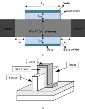
The device structure of double gate n-channel
Fin-FET structure has been illustrated in Fig. 1, which
consists of channel length
L
g(also called gate length),
channel width
W
ch, which is also referred to as fin width
or fin thickness,
T
finin case of triple gate FinFET
where-in top gate is made active by makwhere-ing the top oxide layer
very thin. Further, the oxide is placed on either sides of
Table 1– List of various properties of Si, GaAs, GaSb and GaN channel materials at 300 K undertaken for simulation study [19-21]
S. No.
Properties
Si
GaAs
GaSb
GaN
1
Energy band-gap (eV)
1.12
1.424
0.726
3.2
2
Dielectric constant
11.7
12.9
15.7
8.9
3
Electron affinity (V)
4.05
4.07
4.06
4.1
4
Electron effective mass
0.2
m
00.041
m
00.063
m
00.20
m
05
Density of states
effective mass
Electrons
1.18
m
00.57
m
00.6
m
00.57
m
06
Holes
0.81
m
00.8
m
01.5
m
00.8
m
07
Light-hole effective mass
0.16
m
00.076
m
00.05
m
00.3
m
08
Heavy-hole effective mass
0.49
m
00.050
m
00.4
m
01.4
m
09
Electron mobility (cm
2/V-s)
1450
8500
3000
1000
10
Hole mobility (cm
2/V-s)
500
400
1000
200
11
Saturation Velocity
(cm/s)
Electrons
1.0
10
70.72
10
71.34
10
70.9
10
712
Holes
0.704
10
70.9
10
71.1
10
71.0
10
7the side walls of fin and at the top surface of the fin
before the gate contact is made. The thickness of the
side wall oxide is specified by
t
ox1and
t
ox2. For the
de-vice structure undertaken during the present
simula-tion study, the gate length has been varied in the range
of 40 nm to 55 nm, channel width from 15 nm to
40 nm. The oxide thickness has been taken 2 nm and
kept constant throughout the simulation studies. The
drain / source doping has been kept fixed at
1
10
20cm
– 3and channel doping 5
10
16cm
– 3. The
drain bias has been taken 0.05 V and 1 V, gate bias
varied from 0 V to 1 V.
a
b
Fig. 1– Two Dimensional Double-Gate structure of a FinFET
device (a), Quasi-planar three dimensional structure of Fin-FET on SOI (b)
The results presented are based on drift-diffusion
model. The model has been used in the present
calcula-tions because of the fact that subthreshold
characteris-tics of these devices are diffusion dominated and
re-flects device characteristics in the subthreshold region
well in consistence with the experimentally observed
results [22, 23]. It has been reported that quantum
mechanical effects become negligible while simulating
the transistor structures with lateral dimensions
greater than 10 nm. In the present study, device
simu-lations have been performed using online PADRE
si-mulator from MuGFET tool, developed at Purdue
Uni-versity and is available at nanoHUB [23].
4.
SIMULATION RESULTS
4.1
DIBL versus Gate Length and Channel Width
In order to study the DIBL characteristics with
re-spect to gate length,
L
g, the
n
-FinFET structure has
been simulated with various gate lengths (
L
g) ranging
from 40 nm to 55 nm for a fixed channel width of
30 nm and oxide thickness of 2 nm. The different
channel materials used are Si, GaAs, GaSb and GaN
with the material properties as given in Table 1. DIBL
is a measure of how significantly the potential barrier
in the channel, and hence the conduction path between
source and drain is controlled by drain bias rather than
what should be controlled by gate bias. Generally,
DIBL increases sharply with the decrease in gate
length of FinFET while as it decreases with the
de-crease in channel width. It is because the drain
influ-ence upon the channel potential increases while
de-creasing the gate length or inde-creasing the channel
width. The DIBL versus gate length is plotted in Fig. 2
for the four different materials. From the simulation
study carried out in this work, it has been observed
that GaAs and GaN-channel FinFET structures offer
better DIBL characteristics in comparison with other
materials, however for gate lengths less than about
46nm, GaN offers better characteristics of DIBL
com-pared with GaAs.
Fig. 2– DIBL vs Gate Length (Lg) for Si, GaAs, GaSb, GaN
channel FinFETs for Wch 30 nm and tox1tox2 2 nm
In Fig. 3 simulation results of DIBL variation with
channel width,
W
chof FinFET has been presented,
wherein the gate length and oxide thickness has been
kept constant at 45 nm and 2 nm respectively. For this
study, the channel width has been varied over 20 to
35 nm and the devices were again simulated
individu-ally for different channel materials (Si, GaAs, GaSb
and GaN).
Fig. 3– DIBL vs Channel width (Wch) for Si, GaAs, GaSb and
From the characteristics obtained, it has been
ob-served that GaN channel-FinFET offers better DIBL
characteristics compared with Si, GaSb and GaAs
based FinFETs, however, for channel width less than
about 25 nm, the DIBL characteristics are almost same
for Si, GaAs and GaN-channel FinFETs. Furthermore
GaSb-channel FinFET offers worst DIBL
characteris-tics in both DIBL versus channel length variation and
DIBL versus channel width variation.
4.2
Subthreshold Slope (SS) versus Gate Length
and Channel Width
The study of Subthreshold characteristics becomes
much more important parameter while decreasing the
device dimensions much below in the nanometre
re-gime of operation. It gives insight of the leakage
cur-rents associated with the device characteristics. As
expected in general, for every different device structure
studied, the subthreshold slope increases with the
de-crease in channel length, however it improves with the
decrease in channel width. The variation of
subthresh-old slope (SS) with gate length,
L
gin case of the
n
-FinFET for different channel materials has been
plotted in Fig. 4 while that with respect to channel
width,
W
chis plotted in Fig. 5. For SS study,
L
ghas
been varied from 40 to 55 nm while as
W
chhas been
varied from 15 to 35 nm. It is clear from the results
shown in Fig. 4 that Si and GaAs-channel FinFET
show almost identical SS characteristics, while as the
GaN-channel device offers the better SS characteristics
compared with other three materials. The worst SS
characteristics are obtained for GaSb channel material
structures.
Fig. 4– Subthreshold Slope (SS) vs Gate Length (Lg) for Si,
GaAs, GaSb and GaN channel FinFETs for Wch 30 nm and
tox1tox2 2 nm
From the results shown in Fig. 5, it is clear that for
a channel width of about 18 nm the three materials (Si,
GaAs and GaSb) exhibit same value of the
subthresh-old slope. For channel width greater than about 18 nm,
SS behaviour for Si and GaAs- channel FinFET is
almost same throughout the range of simulation study.
GaN-channel FinFET has shown much better SS
char-acteristics compared with other three channel
materi-als. Furthermore, it may be pointed out that GASb
channel FinFET once again shows the worst SS
char-acteristics compared with other three materials;
how-ever for channel width below 18 nm, GaSb has good SS
characteristics.
Fig. 5– Subthreshold Slope (SS) vs Channel width (Wch) for
Si, GaAs, GaSb and GaN channel FinFETs for Lg 45 nm and
tox1tox2 2 nm
4.3
Threshold Voltage versus Gate Length (
L
g)
and Chnnel Width (
W
ch)
Maintaining a proper threshold voltage for a
par-ticular device is an important technological parameter,
and is adjusted through gate work-function
engineer-ing in case of ultrathin devices like FinFET. Further
the off-state leakage current of a device is associated
with the proper adjustment of its threshold voltage,
which needs to be higher for lower off-state leakages.
In order to study the variation of threshold voltage,
V
twith respect to
L
gand
W
ch, gate length is varied in the
range of 40 to 55 nm while as the channel width is
var-ied in the range of 20 to 35 nm.
As the case should be, in general, it is clear that for
a given channel material, the threshold voltage rolls off
with the reduction in the gate length of the device
structure. It is because when the distance between the
drain and source is reduced with the reduction in gate
length, channel potential becomes more pronounced to
drain electric field encroachment, leading to an earlier
threshold point of gate bias. Similarly for smaller
channel width devices the two side gates (for the case
of a Double Gate FinFET) constitute a strong coupling
effect upon the channel region and as such maintains
the threshold voltage at a higher value.
Fig. 6 illustrates threshold voltage versus gate
length variation for Si, GaAs and GaSb-channel
Fin-FETs. For the study carried out in Fig. 6, the channel
width, W
chis kept constant at 30 nm, while as the
comparison with the other three materials studied.
Further it should be clear from the Fig. 6 and 7, that
the GaSb channel structure once again shows a worst
case of threshold voltage roll-off for both
L
gand
W
chvariations.
Fig. 6– Threshold voltage vs Gate Length (Lg) for Si, GaAs,
GaSb and GaN channel FinFETs for Wch 30 nm and
tox1tox2 2 nm
Fig. 7– Threshold voltage vs Channel width (Wch) for Si,
GaAs, GaSb and GaN channel FinFETs for Lg 45 nm and
tox1tox2 2 nm
5.
CONCLUSION
A comparative study based on short channel
ef-fects viz., DIBL, SS and Threshold voltage roll-off
characteristics has been carried out in this paper for a
FinFET structure utilising different channel
als at every time. For every different channel
materi-al, the SCE’s variation with respect to scaling
param-eters viz., gate length,
L
gand channel width,
W
chhas
been studied. The results generated show that both
GaAs and GaN show better DIBL characteristics with
respect to
L
g, however for
L
g
46 nm GaN offers
bet-ter DIBL characbet-teristics. The DIBL characbet-teristics
with respect to
W
chshow that GaN is better choice,
however for
W
ch
25 nm, the DIBL characteristics are
almost same for Si, GaAs and GaN. Study of SS
char-acteristics with respect to
L
gand
W
chhas shown that
Si and GaAs FinFET has almost identical SS
charac-teristics with respect to
L
gwhile as GaN device offers
better SS characteristics compared with other three
channel materials. At a channel width of 18 nm,
Fin-FET devices based on Si, GaAs and GaSb exhibit
same value of SS, however, for
L
g
18 nm, SS
behav-iour Si and GaAs FinFET is almost same throughout
the range of simulation study. Furthermore GaN has
shown better SS characteristics with respect to
W
ch.
Study of threshold voltage roll-off characteristics has
shown that Si, GaAs and GaN-channel structures
offer almost identical
V
tcharacteristics
with respect to
both
L
g, while as GaN has been shown to offer much
better
V
tcharacteristics with respect to
W
ch. It is
worth noting that GaSb has shown the worst case for
all Short Channel Effect (SCE) characteristics,
how-ever for
W
ch
18 nm, GaSb has shown good SS
char-acteristics. Based on this simulation study it may be
concluded that there is a wide range of research that
needs to undergo for efficiently selecting a channel
material in order to meet the specific requirements of
device design for a particular technology node.
REFERENCES
1. J.P. Colinge, Solid-State Electron.48 No 6, 897 (2004). 2. V. Subramanian, IETE Tech. Rev.27 No 6, 446 (2010). 3. J.P. Colinge, FinFETs and Other Multi-Gate Transistors
(Springer: 2008)
4. http://www.itrs.net/updates
5. D. Hisamoto, et al., IEEE T. Electron Dev.47 No 12, 2320 (2000).
6. Bin Yu, et al., Techl. Digest of IEDM 251 (San Francisco: USA: 2002).
7. S. Oktyabrsky, P.D. Ye, Fundamentals of III-V Semicon-ductor MOSFETs (Springer: 2010).
8. Chen, et al., Nanoscale Res. Lett.7 No 1, 431 (2012). 9. S. Oktyabrsky, et al., Int. J. High Speed Electron. Systems
18 No 4, 761 (2008).
10.A. Ali, et al., Appl. Phys. Lett.97 No 14, 143502 (2010). 11.C. Merckling, et al., J. Appl. Phys. 109 No 7, 073719
(2011).
12.Aneesh Nainani, et al., IEEE T. Electron Dev.58 No 10, 3407 (2011).
13.E.E. Barrowcliff, L.O. Bubulac, D.T. Cheung, W.E. Tennant, A.M. Andrews, IEDM Tech. Dig.23, 559 (1977).
14.Jau-Yi Wu, Hwei-Heng Wang, Yeong-Her Wang,
Mau-Phon Houng, IEEE Elect. Dev. Lett.22 No 1, 2 (2001). 15.H. Chien-Jung, et al., Jpn. J. Appl. Phys. 41 No 9, 5561
(2002).
16.http://en.wikipedia.org/wiki/Gallium_nitride
17.http://en.wikipedia.org/wiki/Aluminium_gallium_nitride 18.Shinichi Hoshi, Hideyuki Okita, Yoshiaki Morino,
Masa-nori Itoh Oki Techn. Rev.74 No 3, (2007).
19.M. Shur, Physics of Semiconductor Devices (PHI-New Delhi: 2004).
20.Palankovski, Vassil, Quay, Rüdiger, Analysis and Simula-tion of Heterostructure Devices (Springer: 2004).
21.Michael A. Kinch, Fundamentals of Infrared Detector Ma-terials (SPIE Publications: 2007).
22.Tai-su Park, Euijoon Yoon, Jong-Ho Lee, Physica E19, 6 (2003).