J. Nano- Electron. Phys.
3 (2011) No1, P. 569-575 (Sumy State University) 2011 SumDU
569 PACS numbers: 85.30.Tv, 85.35. – p
TWO DIMENSIONAL ANALYTICAL MODELING FOR
SOI AND SON MOSFET AND THEIR PERFORMANCE COMPARISON
Saptarsi Ghosh1, Khomdram Jolson Singh2, Sanjay Deb1, Subir Kumar Sarkar1
1 Jadavpur University,
Raja S.C. Mullick Rd., 700032, Kolkata, India E-mail: [email protected]
2 Manipur Institute of Technology,
Takyelpat N.C Rd., 795004,Imphal, India
During last few decade continuous device performance improvements have been achieved through a combination of device scaling, new device structures and material property improvement to its fundamental limits. Conventional silicon (bulk CMOS) technology can’t overcome the fundamental physical limitations belong to sub-micro or nanometer region which leads to alternative device technology like Silicon-on-Insulator (SOI) technology and its recent innovative modification Silicon-On-Nothing (SON) MOSFET. Analytical simulation is very important to understand the relative performance of those devices under different structural and operational parameter variations. For present analytical simulation asymmetric structure of Silicon-On-Insulator (SOI) MOSFET and Silicon-On-Nothing (SON) MOSFET are considered. The proposed structure of SON MOSFET is similar to that of the SOI MOSFET with the only exception being the oxide layer here is substituted with air which has much lower permittivity than Silicon-dioxide. Variation of threshold voltage against effective channel lengths is compared for both the structures. From our simulation it is observed that the proposed SON model has lower drain to source current (IDS) than SOI model. In our modeling based on solution of two dimensional Poisson’s equation short channel effects such as DIBL and fringing field effects are also taken into account. SON is found to provide better suppression of SCE s than SOI. The results predicted by our analytical simulation hold good agreement with experimental results.
Keywords: THRESHOLD VOLTAGE, SOI/SON MOSFET, SHORT CHANNEL EFFECTS, JUNCTION CAPACITANCE, POTENTIAL PROFILE, DIBL, FRINGING FIELD EFFECTS.
(Received 04 February 2011)
1. INTRODUCTION
570 SAPTARSI GHOSH, KHOMDRAM JOLSON SINGH,ET AL.
substrate through the buried layer (BL) [3] is reduced. Reduced coupling effect initiates less SCE s and thus allows further device scaling [4]. Evidently SOI is the better of the two candidates for device miniaturization. It can be scaled to low dimension with the performance not being affected much by SCE. Nowadays a newer proposed model is being considered, namely Silicon-on-Nothing. Here the oxide layer is comprised of air instead of Silicon-dioxide. As air is the highest insulating material only next to vacuum hence SON has better SCE immunity even than SOI. The proposed SON structure exhibits lower drain current and better threshold voltage roll-off for given physical parameters. Our analytical model using Poisson’s equation has been presented for the surface potential leading to the threshold voltage model for the SOI/SON MOSFET. The accuracy of the model is verified by comparing with the experimental results as given by [5].
2. THE ANALYTICAL MODEL
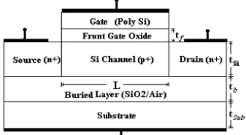
In a short channel device, potential profiles in the channel and beneath the channel (in the BL) are two-dimensional [6]. Threshold voltage of the device can be calculated by solving 2-D Poisson’s equation in the channel [7]. A general layered structure of a SOI MOSFET with polysilicon (n +) as gate is shown in Fig. 1. We take tf, tSi, tb and tsub to be the thicknesses of gate oxide, silicon channel layer, buried layer and the substrate layer, respectively.
Fig. 1 A general SOI/SON-MOSFET layered structure
Also let L be the metallurgical channel length of the device. The 2-D Poisson’s equation applied to the two dimensional channel region of the depleted silicon film body (0 x L, 0 y tSi ) is as in [6],
A
Si
x y x y qN
x y
2 2
2 2
( , ) ( , )
(1)
where, (x, y) is the 2-D potential profile in the silicon channel, NA is the doping concentration of the p-type substrate and Si is the permittivity of silicon.
We consider a second order potential approximation for (x, y) as per Young [8];
TWO DIMENSIONAL ANALYTICAL MODELING FOR… 571
Now let the surface electrostatic potential at the front gate oxide/silicon film interface be sf(x) and that at the back buried oxide/silicon film
interface as sb(x). The four boundary conditions in the channel at the
channel-front gate oxide interface and channel-buried oxide interface, source side and drain side are given as [7];
At y 0,
'
1
( ) ( , )
( ) Ox gs sf
sf
Si Ox
V x
x y
E x
y t (3)
At y tSi,
'
2
( ) ( , )
( ) Ox ss sb
sb
Si Ox
V x
x y
E x
y t (4)
At x 0,
(0,0) sf( ) |x x 0Vbi (5) At xL,
( ,0)L sf( ) |x x LVbi VDS (6) where Si and Ox are dielectric permittivity of silicon and oxide, respectively. Vgs and Vss are the effective front gate to source and substrate to source voltages.
Vgs Vgs Vffb, Vss Vss Vbfb
Vffb and Vbfb being the front and back gate flatband voltages respectively.
Solving Eqn. (1) and (2) with the first two boundary conditions (Eqn. 3 & 4) we get the threshold voltage as [6, 7, 9];
'
1 (2 ) 1 2
2
f f Si
F A Si
b Si b ss
th ffb
f f f f f f
Si
b Si b Si b Si
c c c
qN t
c C c V
V V
c c c c c c
c
c C c C c C
(7)
where, Vth represents the long channel threshold voltage and F kT q N nA i
2 ln( ) is the Fermi potential in the silicon film. Now Vss is modified into Vsseff as,
2 2
0 2
Ox
sseff ss ds
t
V V kV rE L
L (8)
572 SAPTARSI GHOSH, KHOMDRAM JOLSON SINGH,ET AL.
bi ds bi
Si f Ox
sseff ss ds
Si b
L
V V V V V
c c
t
V V kV r L
L c c L 2 2 2
( ') ( ') cosh
2 2 sinh (9)
Putting Vsseff in the Eqn.7 we will get the expression of modified threshold voltage as; '
1 (2 ) 1 2
2
f f Si
F A Si
b Si b sseff
theff ffb
f f f f f f
Si
b Si b Si b Si
c c c
qN t
c C c V
V V
c c c c c c
c
c C c C c C
(10)
Now using last two boundary conditions (Eqn. 5 & 6) we get the actual short channel threshold voltage as;
1 1 2 3 2 1 F
thsc theff F
K V V K K K (11) Where, bi ds
L x x x
V V
K
L
min min min
1
sinh sinh sinh
sinh
L x x
K L min min 2 sinh sinh 1 sinh 3 1 f f b Si f f b Si c c c C K c c c C
The drain current is formulated from threshold voltage as per [6] where
2 1 ( ) 2 1 sff f
GS th DS DS
DS
c
W U
IDS V V V V
V L
LE
(12)
TWO DIMENSIONAL ANALYTICAL MODELING FOR… 573
2
1
( )
2 1
sff f
GS th DSsat DSsat DSsat
c
W U
IDS V V V V
V L
LE
(13)
in the saturation region.
where EC is the critical field at which electron velocity (ve) saturates and
VDS,sat is the saturation voltage and both are given by, s
c v E
,
1
GS th DSsat
GS th
c
V V
V
V V
LE
3. RESULTS AND DISCUSSION
In bulk MOSFET only front interface surface potential sf is affects the threshold voltage whereas in short channel SOI structure, sf as well as back interface sbstrongly influences the threshold voltage. Here performance of SOI structure is simulated with respect to the threshold voltage which can be explained on the basis of relative coupling of front and back interface potential. Significant modification of sb in SON structure due to lowest dielectric constant material (air) in the box region will initiate signification performance variation over SOI structure. Whole set of results presented here, regarding the threshold voltage and drain current can be explained on the basis of relative variation of front and back interface potential. Value of potential coupling ratio (PCR sf/sb) gives an estimation of SCEs and on the basis that performance of SOI and SON structures are compared. Higher PCR initiates less SCEs specially DIBL which can be initiated with higher sfor lesssb.
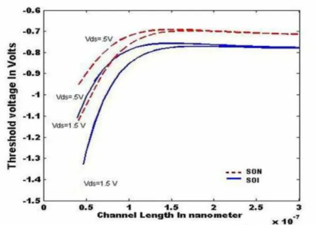
Increasing channel length shifts the short channel device towards bulk. With increasing channel length the value of the minimum surface potential reduces further therefore increasing the threshold voltage. SON suffers lesser potential coupling than SOI due to the fact air having much higher permittivity than Silicon-dioxide. Evidently SON has higher threshold voltage than SOI. From Fig. 2. it is quite clear that SON structure shows improvement in Threshold Voltage Roll-Off (TVRO) compared to SOI structure.
574 SAPTARSI GHOSH, KHOMDRAM JOLSON SINGH,ET AL.
Fig. 2 – Threshold Voltage variation against diff. channel lengths for applied VDS 5 Volts and 1,5 Volts
Fig. 3 – Variation of drain current against drain to source voltages for gate to source voltages of 2 Volts, 2,5 Volts and 3 Volts
4. CONCLUSION
A generalized threshold voltage model for SOI/SON-MOSFET is developed by solving 2-D Poisson’s equation in the channel region and analytical expressions are also developed for the same. The performance of the devices is studied with respect to threshold voltage and drain current. Of the two devices for the same dimension and parameters SON has more threshold voltage and lower drain current. But to reduce PCR further material with
TWO DIMENSIONAL ANALYTICAL MODELING FOR… 575
REFERENCES
1. T. Ohno, Y. Kado, M. Harada, T. Tsuchiya, IEEE T. Electron. Dev. 42, 1481 (1995). 2. T.C. Hsiao, J.C.S Woo, IEEE T. Electron. Dev. 42, 1120 (1995).
3. T. Sato, H. Nii, M. Hatano, K. Takenaka, H. Hayashi, K. Ishigo, T. Hirano, K. Ida, Y. Tsunashima, IEIC Technical Report 102,99 (2002).
4. V. Kilchytska, T.M. Chung, B. Olbrechts, Ya. Vovk, J.-P. Raskin, D. Flandre,
Solid-State Electron. 51, 1238 (2007).
5. M.C. Hu, S.L. Jang, Int. J. Electron.84,167 (1998).
6. K. Suzuki, S. Pidin, IEEE T. Electron. Dev.50, 1297 (2003). 7. G. Zhang, Z. Shao, K. Zhou, IEEE T. Electron. Dev. 55, 803 (2008). 8. K.K.Young, IEEE T. Electron. Dev. 36, 399 (1989).