Abstract— In recent years, the aggressive scaling of CMOS technology has reduced the associated geometry to very low dimensions. At the same time, this process is accompanied inevitably with an increased reliability concern expressed basically by the ageing degradation that is a well-recognized challenge for further MOSFET family scaling. In this work, an Adaptive Network Fuzzy Inference System (ANFIS) based approach is proposed to model the relative degradation of the threshold voltage caused by the hot carrier effect. The DG MOSFET device under study is subject to both short channel and quantum confinement effects which make the direct application of analytical tools a very hard task to achieve. The obtained results show good agreement with numerical simulations (Atlas 2D-simulator) so that the proposed approach might serve as a basis for more complex degradation behavior modeling frameworks.
Index Terms— Nanoscale DG MOSFET, threshold voltage, hot carrier degradation, short channel effect, fuzzy modeling.
I. INTRODUCTION
or today’s computer product industry, the need for highly packaged devices is arising as an ultimate goal especially for VLSI chips such as microprocessors and semiconductor memories [1]. So, more efforts should be dedicated to the performance analysis of new proposed structures. As stated by the International Technology Roadmap of Semiconductors (ITRS), the Metal Oxide Semiconductor Field Effect Transistor (MOSFET) has reached an advanced level of development thanks to the adoption of many improvements such as multi-gate geometries and high-k materials, which has allowed remedying to many anomalies and drawbacks [2]. Despite these enhancements, a similar situation arises again for the
T. Bentrciais with the Laboratory of Advanced Electronic, Department of Electronics, University of Batna, 05000, Algeria (e-mail: [email protected]).
F. Djeffalis with the Laboratory of Advanced Electronic, Department of Electronics, LEPCM, University of Batna, 05000, Algeria (e-mail: faycaldzdz@ hotmail.com).
M. Meguellatiis with the Laboratory of Advanced Electronic, Department of Electronics, University of Batna, 05000, Algeria (e-mail: m_meguellati @yahoo.fr).
D. Arar is with the Laboratory of Advanced Electronic, Department of Electronics, University of Batna, 05000, Algeria (e-mail: [email protected]).
widely used multi-gate transistor called Double Gate (DG) MOSFET when the device is scaled below the 100 nm technology node [3]. This is can be explained by the fact that the Short Channel Effects (SCEs) are aggressively amplified proportionally to the dimension reduction affecting hence various device parameters considerably [4].
Although the DG MOSFET downscaling trends are currently a major research subject, the reliability aspect related to such reduction of the device dimensions is also becoming a heavy concern for the design engineer community. This reliability aspect consists in the creation of interface traps under the hot carrier injection effect due to the increase of the maximum electric field experienced by the carriers in the channel region near the drain end since the associated power supply voltages scale at a slower rate than channel lengths. As the carriers move from the source to the drain side, they can attend sufficient kinetic energy in the high field region of the drain junction and initiate an impact ionization process. A portion of them can even pass the Si-SiO2 potential barrier and penetrate into the gate oxide [5]. So, the hot carriers are characterized by the violation of the thermal equilibrium with the lattice in addition to an energy gain higher than the thermal energy. After a long duration of the device function, the accumulation of the injected carriers leads to interface trap buildup and the trapping of carriers in the dielectric, which can initiate in turn the degradation of the main device parameters such as the threshold voltage [6]. Therefore, the carrier trapping mechanism in short channel MOSFETs is seen as the principal origin of instability and is considered as one of the serious obstacles facing the next generation MOS integrated circuit development.
The accurate modeling of symmetrical DG MOSFET behavior with both ultrathin Silicon body and short channel length requires two or three dimensional solutions of the coupled Schrodinger/Poisson equations which can be solved only by numerical methods because of the nature of the physical effects governing the electrical behavior of these devices [7]. The deduction of a closed form analytical formulation valid in all operating regions of interest is a very difficult, even an impossible task to achieve. As a result, other alternative approaches have been proposed to model DG MOSFET performances against the hot carrier degradation when subject to quantum effects.
New Approach Based on ANFIS Computation to
Study the Threshold Voltage Behavior Including
Trap Effects for Nanoscale DG MOSFETs
T. Bentrcia F. Djeffal, M. Meguellati and D. Arar
The main goal of this paper is to explore the capabilities of Adaptive Network based Fuzzy Inference Systems (ANFISs) to be used as a predictor for the relative degradation of DG MOSFET threshold voltage. Both the hot carrier and quantum effects are taken into account where two geometrical parameters are selected as input variables to the fuzzy system. By adopting such methodology, several types of membership functions are tested and the best one in term of accuracy is selected.
The paper is organized as follows: First, we provide some elementary models expressing the alteration of the threshold voltage as a result of some miniaturization effects. Then, we illustrate the main phases of ANFIS methodology. After, the elaboration and the organization of the data set used for the training of our fuzzy system are investigated. Results are detailed in the fifth section and we terminate with some remarks and future work directions.
II. INFLUENCE OF DOWNSCALING EFFECTS ON THE
THRESHOLD VOLTAGE
With the present day continuous downscaling of electronics devices, the threshold voltage of a MOSFET device, which defines the gate voltage needed to be applied in order to make the device turn on, is strongly influenced by various effects generated by such process of miniaturization [8, 9]. For this reason, it is highly recommended to model the threshold voltage accurately so that the correct behavior of new designed circuits could be predicted appropriately.
The ageing of MOSFET devices because of the long duration of function is reflected by damages in the form of interface traps created by hot carriers in the channel. Many papers have been dedicated to the modeling of MOSFET devices including interface traps and various analytical compact models have been proposed [10-12]. The presence of an interface charge density causes an increase in the threshold voltage to give an additional term in the model of the fresh device defined as [13]
ox it 0 th C Q Q
V
(1)
where Q0 is the trapped charge density in the oxide, Qit is the interface trap charge density and Cox is the oxide capacitance. It can be concluded that the device becomes less sensitive to biasing and higher gate voltages are required to switch the device from the OFF-state to the ON-state.
If we consider now the geometrical parameters, experimental results show that when the channel length becomes small, the threshold voltage changes from its long channel values and decreases with decreasing channel lengths. This monotone reduction becomes more noticeable when the channel length becomes comparable to the source and the drain depletion widths. The change in the threshold voltage due to the short channel effect is given by [14]
1 X X 2 1 L X C Q V j dm j ox b th
(2)
where Qb is the bulk charge per unit area, Xj is the junction depth and Xdm is the maximum depletion width.
For the more general case when both device width and length are of the same order of magnitude as the depletion width (small geometry device), the shift in the threshold voltage induced by small geometry effect can be approximated by the superposition of the short channel and narrow width effects as follows [15]
W , th L , th
th V V
V
(3) The consequence of quantization is that the distribution of accumulated or inverted carriers at the interface is different from the classical prediction [16], which affects directly any surface potential deduced parameter. The quantum confinement effect is significant for oxide and channel thicknesses of the order of nanometer. Therefore, the inclusion of quantum effects in the modeling framework cannot be excluded in this situation. The threshold voltage shift due to quantum effects can be expressed by [17]
2 / 1 i si ox A ox th n kT 2 N t V
(4)
where β is a fitting parameter, tox is oxide thickness, NA is the channel doping concentration and ni represents the intrinsic carrier concentration.
III. ANFIS METHODOLOGY
The main idea behind the elaboration of artificial intelligence based models for electronics applications is founded on input-output mapping, where an equivalent schema is developed with a set of adjustable parameters. These parameters are tuned up using a learning algorithm to get a good matching between the predicted and measured responses.
The ANFIS structure considered as a multilayer feed forward network was proposed initially as a combination of fuzzy logic and artificial neural networks [18]. Accordingly, ANFIS possess both advantages of the neural network learning capability and the structured knowledge representation employed in fuzzy inference systems. This approach was successfully applied in many fields mainly for nonlinear inverse mapping and time series prediction. In the pioneer work of Jang [19], it is proved that ANFIS is a universal competitive approximator when compared to many other existing approaches.
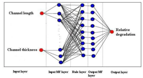
The cornerstone of such methodology consists in the division of the input space into many local subregions that several of them can be activated simultaneously by a single input. These subregions are obtained by a partition procedure of the input space using fuzzy membership functions [20]. If we limit the input variables of our fuzzy system to the channel length and thickness having both a significant influence on short channel and quantum effects, the ANFIS model is similar to the structure represented in figure 1.
Layer 1: the output of each node gives the input variable membership grade.
Layer 2: the firing strength associated with each rule is calculated.
Layer 3: the calculation of the relative weight of each rule is achieved.
Layer 4: the multiplication of normalized firing strength by first order of Sugeno fuzzy rule is realized.
Layer 5: one node is composed and all inputs of the node are added up.
Fig. 1. Structure of ANFIS proposed for the estimation of the relative degradation in the threshold voltage.
It should be noted that there are only two adaptive layers; the first one includes modifiable parameters pertaining to the input membership functions known as the premise parameters. The second one represented by the fourth layer contains modifiable parameters called consequent parameters of the linear model. The number of fuzzy sets attached to each input is denoted by n and m respectively. The number of Takagi-Sugeno fuzzy IF-THEN rules is n×m. The generic expression of such rules is given by
l si l l l 0 th
th j
si
i V p L qt r
V THEN B is t AND A is L
IF (5)
Ai and Bj are the linguistic terms of the precondition part with membership functions µAi(L) and µBj(tsi) respectively. The parameters pl, ql and rl denote the consequent parameters.
The hybrid learning algorithm used in ANFIS combines the gradient method with the least square method to update the parameters, where a generic parameter α formed by the union of the premise and the consequent parameters is updated using the formula
E (6) where E is the overall error and η is a learning rate adjusted according to
2
E
(7)
where δ is the step-size.
During the training phase, the generic parameter is modified at each training epoch in a hybrid manner. More specifically, the consequent parameters are updated first using
a least square algorithm and the premise parameters are then adjusted by backpropagating the errors [21].
IV. TRAINING DATABASE ELABORATION
In order to evaluate the DG MOSFET immunity against the hot carrier degradation taking into account the quantum confinement in addition to short channel effects, various channel lengths and thicknesses are used to estimate the range of effects that may be more interesting for analysis. The threshold voltage corresponding to a structure with specified
dimensions is obtained using Atlas 2-D device simulator [22]. The geometrical and electrical configuration of the simulated DG MOSFET is expressed by the set of values provided in table 1.
The corresponding two-dimensional layout is illustrated in the following sub-section. The device has uniform doping concentrations for both channel and source/drain regions. Two carrier types are used in the simulation, the drift-diffusion model without impact ionization, doping concentration-dependant carrier mobility and electric field-dependant carrier model are also adopted. To take into consideration the leakage current, SRH recombination/generation is included in the simulation. Figure 2 illustrates a cross-sectional view of the DG MOSFET device used in this work.
Fig. 2. Schematic view of the symmetrical DG MOSGET including interface traps.
In figure 3, we highlight the relative disposition of the
TABLEI
DEVICE DESIGN AND SIMULATION PARAMETERS.
Parameter Value
Oxide thicknesse 1.5 nm
Drain/Source doping 1×1020 cm-3
Channel doping 1×1015 cm-3
Workfunction 4.55 eV
Interface trap density 5×1012 cm-2
Drain voltage 0.1 V
threshold voltage curves for fresh and damaged cases as obtained using Atlas 2-D Simulator. For both cases, the variation law is monotonic with the channel length until the parameter reaches a saturation value. It can be noticed that the damaged device has higher threshold voltage due to the increase of the applied gate voltage needed to make the device turn on. Another interesting feature related to the discrepancy of curves, which is more important for short channel length values compared to long channel lengths. Such situation can be interpreted by the strong correlation existing between the hot carrier degradation and the short channel effect.
30 40 50 60 70 80 90 0.32
0.34 0.36 0.38 0.40 0.42 0.44 0.46 0.48 0.50 0.52
Th
re
sh
ol
d
vo
lta
ge
[V
]
Channel length [nm] Fresh DG MOSFET
DG MOSFET including interface traps
Fig. 3. Threshold voltage variation as function of the channel length for fresh and damaged devices.
V. RESULTS AND DISCUSSIONS
Due to the importance of the elaboration of a suitable and complete database for the ANFIS training, the training set must be extended as much as possible in the whole input-output space of data. The incompleteness of the selected set reduces the ability of the network when it encounters an unknown pattern. The data set used for the training of our fuzzy system is obtained by the numerical simulator ATLAS. Since the accuracy of the trained ANFIS depends on the precision and the effective representation of the data, which will be used in the training process, a total of 91 data sets are obtained by sampling the channel length and the channel thickness ranges with a step of 5 nm and 0.5 nm, respectively. The membership functions have a strong influence on the performances of the decision system. So, an optimal determination of these functions is indispensable. However, the only solution is the trial and error approach because of the absence of any well-established method that allows the specification of membership functions in the ANFIS. In this work, three different types of membership functions with Gaussian-Shaped, Bell-Shaped and Pi-Shaped are selected due to their wide utilization and verified empirically. The best fuzzy membership function configuration generating the best result is chosen for the calculation of the relative degradation occurring in the threshold voltage. The Pi-Shaped membership function is finally selected as it is associated with the best values for the mean square error and the correlation
coefficient.
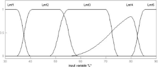
The number of the membership functions for the input parameters is fixed to 5 for the channel length and to 10 for the channel thickness which gives a number of fuzzy IF-THEN rules for the fuzzy inference system equals to 50 (5×10). The examination of the obtained results indicates that the use of the Pi-Shaped membership function gives higher performances compared to the Gaussian-Shaped or the Bell-Shaped membership functions. The partition of the input variables using the best obtained membership function is illustrated in figures 4 and 5.
Fig. 4. Pi membership functions of the channel length parameter (L).
Fig. 5. Pi membership functions of the channel thickness parameter (tsi).
Fig. 6. ANFIS response surface.
The scatter diagrams of the predicted and numerical values of the threshold voltage relative degradation are presented in figures 7 and 8 for the training and testing data sets. It is easy to note that a sufficient agreement is satisfied between the predicted and numerical results.
Fig. 7. Regression curve of the threshold voltage for the training data set.
Fig. 8. Regression curve of the threshold voltage for the testing data set.
A summary of the main performance criteria for both training and testing phases is provided in the following table.
TABLEII
PERFORMANCE CRITERIA FOR THE TRAINING AND TESTING PHASES.
Criterion Training Testing
Criterion Training Testing
Mean square error 4.94×10⁻⁴ 3.83×10⁻²
Correlation coefficient 0.99 0.702
As can be deduced from this table, the correlation coefficient for the testing set is comprised between 0.7 and 0.9. Such value indicates that we have a strong high correlation between the predicted and the measured degradation values of the threshold voltage. Thus, the performance of our fuzzy system is acceptable and it can be used for further analysis of DG MOSFETs employed in IC design applications.
VI. CONCLUSION AND FUTURE WORK
In this paper, the prediction of the relative degradation in the threshold voltage of DG MOSFET under hot carrier, short channel and quantum confinement effects is studied using an ANFIS based approach. The channel length and thickness have been considered as input variables because of their strong influence on considered effects. Thanks to the numerical results generated using 2D-ATLAS simulator, it was possible to elaborate the required training database, where a hybrid learning algorithm has been used to adjust various premise and consequent parameters. The obtained performances have demonstrated that the developed fuzzy logic based approach is particularly suitable to be implemented in electronics device simulators to study the CMOS circuits at nanoscale level when heterogeneous constraints are included within the whole framework. Therefore, fuzzy logic can be considered as an efficient tool that permits the alleviation of many drawbacks related to the quantum effects inevitable in new generations of nanoscale devices. It should be noted that our proposed approach can be extended to include other device parameters such as the oxide thickness parameter so that the device behavior can be modeled with more precision.
REFERENCES
[1] Y. Zhang, and M.H. White, “A quantum mechanical mobility model for scaled NMOS transistors with ultra-thin high-K dielectrics and metal gate electrodes,” Solid-State Electronics, vol. 52, pp. 1810–1814, 2008. [2] International Technology Roadmap for Semiconductors (ITRS), Published
online at http://public.itrs.net, 2009.
[3] M. A. Abdi, F. Djeffal, M. Meguellati, D. Arar, “Two-dimensional analytical threshold voltage model for nanoscale Graded Channel Gate Stack DG MOSFETs,” 16th IEEE International Conference on Electronics, Circuits, and Systems, ICECS’2009, Hammamet, Tunisia, Dec. 13-16, 2009.
[4] B. Benbakhti, J.S. Ayubi-Moak, K. Kalna, D. Lin, G. Hellings, G. Brammertz, K. De Meyer, I. Thayne, and A. Asenov, “Impact of interface state trap density on the performance characteristics of different III–V MOSFET architectures,” Microelectronics Reliability, vol. 50, pp. 360– 364, 2010.
[5] M.P. Pagey, Hot-carrier reliability simulation in aggressively scaled MOS transistors, PhD Dissertation, Vanderbilt University, Tennessee, USA, 2003.
Signals, Circuits and Systems SCS’2009, pp. 1-6, Djerba, Tunisia, November 06-08, 2009.
[7] F. Prégaldiny, C. Lallement, and D. Mathiot, “Accounting for quantum mechanical effects from accumulation to inversion, in a fully analytical surface-potential-based MOSFET model,” Solid-State Electronics, vol. 48, pp. 781–787, 2004.
[8] T.P. Wen, and A. K. Singh, “A comprehensive analytical study of an undoped symmetrical double-gate MOSFET after considering quantum confinement parameter,” Microelectronics Journal, vol. 41, pp. 162–170, 2010.
[9] B. Dubois, J-B. Kammerer, L. Hebrard, and F. Braun, “Modelling of hot-carrier degradation and its application for analog design for reliability,” Microelectronics Journal, vol. 40, pp. 1274–1280, 2009.
[10] F. Djeffal, T. Bentrcia, and T. Bendib, “An analytical drain current model for undoped GSDG MOSFETs including interfacial hot-carrier effects,” Physica Status Solidi C, vol. 8, pp. 907–910, 2011.
[11] F. Djeffal, T. Bentrcia, M.A. Abdi, and T. Bendib, “Drain current model for undoped gate stack double gate MOSFETs including the hot-carrier degradation effects,” Microelectronics Reliability, vol. 51, pp. 550–555, 2011.
[12] T. Bentrcia, F. Djeffal, and A. Benhaya, “Continuous analytic I-V model for GS DG MOSFETs including hot-carrier degradation effects,” Journal of Semiconductors, vol. 33, pp. 014001:1–014001:6, 2012.
[13] S. Naseh, M.J. Deen, and C-H. Chen, “Hot-carrier reliability of submicron NMOSFETs and integrated NMOS low noise amplifiers,” Microelectronics Reliability, vol. 46, pp. 201–212, 2006.
[14] N. Arora, MOSFET modeling for VLSI simulation theory and practice, Singapore: World scientific publishing, 2007.
[15] C. Galup-Montoro, and M.H. Schneider, MOSFET modeling for circuit analysis and design, Singapore: World scientific publishing, 2007. [16] M. Balaguer, J.B. Roldan, L. Donetti, and F. Gamiz, “Inversion charge
modeling in n-type and p-type Double-Gate MOSFETs including quantum effects: The role of crystallographic orientation,” Solid-State Electronics, vol. 67, pp. 30–37, 2012.
[17] H.C. Morris, H. Abebe, “A compact quantum surface potential model for a MOSFET device,” Mathematical and Computer Modelling, vol.51, pp. 893–900, 2010.
[18] M. Singh, Adaptive network-based fuzzy inference systems for sensorless control of PMSG based wind turbine with power quality improvement features, PhD dissertation, Quebec University, Montreal, Canada, 2010. [19] J. Jang, “ANFIS: adaptive-network-based fuzzy inference system,” IEEE
Transactions on Systems, Man and Cybernytics, vol. 23, pp. 665–685, 1993.
[20] S.M. Aminossadatia, A. Kargarb, and B. Ghasemi, “Adaptive network-based fuzzy inference system analysis of mixed convection in a two-sided lid-driven cavity filled with a nanofluid,” International Journal of Thermal Sciences, vol. 52, pp. 102–111, 2012.
[21] A. Azadeh, S.M. Asadzadeh, and A. Ghanbari, “An adaptive network-based fuzzy inference system for short-term natural gas demand estimation: Uncertain and complex environments,” Energy Policy, vol. 38, pp. 1529–1536, 2010.
[22] Atlas User Manual: Device Simulation Software, 2008.