Brazilian Journal of Physics, vol. 36, no. 3B, September, 2006 809
Transport Properties of a
Ga
1−xMn
xAs
/
Ga
1−yAl
yAs
Double-Barrier
C. F. Ritter∗, S. S. Makler∗, and I. C. da Cunha Lima† ∗Instituto de F´ısica, Universidade Federal Fluminense,
Av. Gal. M. T. de Souza s/n, 24210-340, Niter ´oi, RJ, Brazil †Instituto de F´ısica, Universidade do Estado de Rio de Janeiro,
Rua S˜ao Francisco Xavier 524, 20550-013, Rio de Janeiro, Brazil
Received on 8 December, 2005
We study the transport properties of a spin filter consisting of a double-barrier resonant tunneling device in which the well is made of a semimagnetic material. Even if the device could be made of several materials, we discuss here the case of a Ga1−xMnxAs/Ga1−yAlyAs system because it can be integrated into the well
knownAlAs/GaAstechnology. We solve the HamiltonianH =HK+HP+HE+HM+Hh−i+Hh−h.Its terms represent the kinetic energy, the double-barrier profile, the applied bias, the magnetic interaction, the hole-impurity attraction and the hole-hole repulsion, respectively. A very simple one-dimensional Green function is introduced to solve self-consistently the Poisson equation for the profile due to the charge distribution. A real space renormalization formalism is used to calculate exactly the currents. In a previous work we have shown that the Rashba effect is weak. Therefore the results show very well defined spin-polarized currents. Our results confirm that this system is a good device for spintronics.
Keywords: Double barrier spin polarizer; Diluted magnetic semiconductors; Spintronic devices
I. INTRODUCTION
The system studied here consists of a double-barrier in which the well is made of a diluted magnetic semiconduc-tor (DMS). The magnetization of the well produces resonant peaks that have well defined spin polarization. Therefore the current tunneling through the structure is also spin polarized. The device could be made of several materials. We discuss here the case of aGa1−xMnxAs/Ga1−yAlyAssystem because
it can be integrated into the well knownAlAs/GaAs technol-ogy.
The Mn2+ cations have a magnetic moment due to their spinS=5
2~. In addition, TheMnion binds a hole to satisfy charge neutrality. Homogeneous samples ofGa1−xMnxAs
al-loys withxup to 10% have been produced by molecular beam epitaxy at low temperatures, avoiding the formation ofMnAs clusters that could turn the material to be non-magnetic [1–3]. This kind of DMS introduces an interesting problem from the physical point of view: Mnin the alloy is a strongpdopant, the free hole concentration reaching even p=1020−21cm−3. At smallMnconcentrations, the alloy is a paramagnetic in-sulator. As x increases, it becomes ferromagnetic, going through a non-metal/metal transition for higher concentrations (x≈0.03) and keeping its ferromagnetic phase. Forxabove 5%, the alloy becomes a ferromagnetic insulator. In the metal-lic phase, the ferromagnetic transition is observed in the range of 30−110K, depending on the value ofx. In samples of Ga1−xMnxAswith selectivep−doping [12] it was reported a
Curie temperatureTc∼172K. Today it is possible to make
semiconductors that are ferromagnetic at room temperature [4–7]. Several spintronic devices like spin valves, spin filters, polarizers and analyzers have been made using heterostruc-tures including DMS [8–11].
II. SELF-CONSISTENT PROFILE AND LEVELS
Our tight-binding Hamiltonian is
H
=H
K+H
P+H
E+H
M+H
h−i+H
h−h. (1)where
H
K is the kinetic energy,H
P describes the double-barrier profile andH
E represents the electric field due to the applied bias. The magneticH
M, the hole-impurityH
h−i and the hole-holeH
h−hterms are included in the mean field approximation. The profile and the charge distribution are calculated self-consistently by solving the Poisson equation∇2φ=−ρ/ε, whereρ=ρ
i+ρh includes both the impurity
and hole contributions. This potential gives a contribution
H
h−i+H
h−h=eφ. (2)As the Hamiltonian is modified by this term so are modified its wave functions, from which the hole charge densityρhis
calculated.
Usually the Poisson equation is solved in the momentum space because it becomes an algebraic equation. On the other side, to solve the Hamiltonian (1) in the reciprocal space re-quires a big computational effort. In the context of a tight-binding calculation it is natural to express the Poisson equa-tion in a finite difference formalism, in which it turns out to be a simpleN×Nmatricial equation,
φj−1−2φj+φj+1=− a2
ερj, (3)
whereais the distance between layers. The inverse operator of the discretized one-dimensional Laplacian (its Green func-tion) is obtained easily as
Gi j=−
1
810 C. F. Ritter et al.
and it is symmetric. Using this Green function it is easy to obtain the potential as
φj=− ε
a2 N
∑
k Gjkρk.
Let us discuss now the mean field approximation used for the magnetic term. The hole interaction with the magnetic impurities is described through the contact potential,
H
M(r) =−INi
∑
i=1s(r).S(Ri)δ(r−Ri),
whereI is thep−d exchange coupling constant,Ridenotes the positions of theNi impurities ofMn,S(Ri)is the (clas-sical) spin of the impurity, ands(r)is the spin of the hole. We assume the layer in its metallic and ferromagnetic phase. Thus, the spin of the hole is well defined in that direction, be-ing polarized either up (parallel) or down (anti-parallel). In order to write the magnetic term in the new basis we have to integrate overr. To do that, the magnetic impurities are as-sumed to be uniformly distributed in theGa1−xMnxAsDMS
layer, having the same magnetization<M>. Therefore, a net Mnmagnetization<M>polarizes the hole gas by introduc-ing an additional effective confinintroduc-ing potential given by
H
M(z) =−N0βx(σ/2)<M>,for z inside the well. Here σ=±1 for the hole spin and N0β=I/v0.
III. THE SPIN POLARIZED CURRENTS
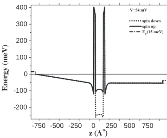
We are dealing here with an open system, but the Hamil-tonian given by equation (1) is first solved in a finite region including the double barrier and a small part of the contacts where the band bending, due to charge accumulation, occurs. This region can be seen in Fig. 1.
Outside this region the profile is flat. Therefore the solu-tions are plane waves for energies above the Fermi level and evanescent modes below it. The total Hamiltonian can be writ-ten as
H
=H
0+H
1, whereH
0=H
L+H
S+H
R describes three uncoupled regions: the left contact, the scattering region and the right contact. Thus each part ofH
0can be diagonal-ized exactly.The diagonalization of
H
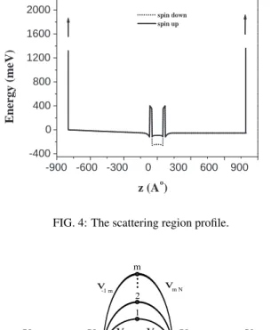
S yields the spin polarized reso-nant levels shown in Fig. 2. Besides, other non-resoreso-nant states are obtained that are necessary to get the exact solution.We shall connect the three regions depicted in Fig.3 to get the exact solution for the open system. This method is the extension of the standard procedure described in elementary quantum text books, to the tight binding formalism.
For this device the scattering region for each spin is de-picted in Fig. 4. To relate the plane wave amplitudes at right
-750 -500 -250 0 250 500 750
-200 -100 0 100 200 300
400 V=54 mV
spin down spin up EF(15 meV)
Energy (meV)
z (Ao)
FIG. 1: The self-consistent potential for an applied biasV=54mV
-150 -100 -50 0 50 100 150
-200 -100 0 100 200 300 400
AlAs AlAs Ga1-xMnxAs
GaAs GaAs
V=54 mV
spin down spin up EF(15 meV)
doublet
Energy (meV)
z (Ao)
FIG. 2: The resonant levels.
and left of the double barrier we reconnect the three regions using the Hamiltonian
H
1=v(c+−1c0+c+0c−1) +v(c+N−1cN+c+NcN−1)wherevis the hopping that gives the effective massm∗. Here the left region goes from−∞to−1, theNsites from 0 toN−1 belong to the scattering region and labels fromNto∞ corre-spond to the right region. By labelingm=0, . . . ,N−1 the scattering region eigenstates, that come out from the numer-ical diagonalization of
H
S, we can represent the reconnected regions by the diagram of Fig.5.... J ... 2 N N+1 ... J ...
H
H
H
1
− − −
R S
L
Brazilian Journal of Physics, vol. 36, no. 3B, September, 2006 811
-900 -600 -300 0 300 600 900 -400
0 400 800 1200 1600
2000 spin down
spin up
Energy (meV)
z (Ao)
FIG. 4: The scattering region profile.
FIG. 5: The scheme for reconnection.
Here,v¯1m=h¯1|
H
1|mi=vh¯1|miare the hoppings from the left contact to the levels of the scattering region. In similar way we getvm1=vhm|1i. It is easy to see thathm|1i=uNm,i. e., the last component of the m-th eigenvector.
Now it is easy to decimate all the states in the well. The result is a renormalization of the energies at sites -1 and N and the effective hopping between them. We get
˜
ε¯1 = ε¯1+
∑
mv2¯1m/(~ω−Em)
˜
εN = εN+
∑
mv2mN/(~ω−Em)
˜
v¯1N =
∑
m
v¯1mvmN/(~ω−Em)
where we denote the site−1 as ¯1 to simplify the notation. After that, we obtain directly the transmittance and there-fore the current.
We emphasize that this procedure is non-perturbative. Thus the results are exact. The diagram representing the renormal-ized equations is shown in Fig. 6, where we have renamed the layers fromNto∞as 1,2, . . . ,∞.
Now the solutions at the emitter (layers ¯1 and ¯2) can be easily connected with the solutions at the collector (Layers 1 and 2) to obtain the transmittance. Finally we get the current using the Landauer-B¨utiker formalism.
1
2
...
...
v
−
1
−
v
~
ε
− 11
v
~2
1 −
~
ε
1ε
2− 2
ε
FIG. 6: The renormalized diagram.
IV. RESULTS
Due to the very high hole density inside the well, a simple iterative procedure to get selfconsistency does not converge. Instead, a quasi-Newton procedure for solving non-linear sys-tems is used. It requires to diagonalize
H
S many times for each applied potential. However the diagonalization ofH
Sis very fast because it is a finite tridiagonal matrix.After this process, the selfconsistent profile and the spin po-larized levels shown in Fig.2 are obtained. Through the pro-cedure described in the previous section we get the electronic current as a function of the applied bias shown in Fig.7. It is easy to see that the three polarized levels above the Fermi in Fig.2 begin to descend. When one of these levels is in be-tween the Fermi level and the bottom of the band a current peak appears.
20 40 60 80 100
0 3 6 9 12 15 18
Current (mA)
bias(mV)
spin down spin up
FIG. 7: The spin polarized currents.
V. CONCLUSIONS
812 C. F. Ritter et al.
As discussed in previous works [13–15] the device described here produces a current strongly polarized. Without taken into account the Rashba effect, the polarization is almost total. The only spin mixture is due to the very small tail of a −σtransmittance peak at the central region of aσpeak. In a previous work [21] the peaks were not completely polarized because we considered the Rashba effect at the well walls that flip the spin of the carriers. Nevertheless this effect is quadratic in the small Rashba parameterα. Therefore the depolarization is small.
We conclude that a double-barrier heterostructure with a
diluted ferromagnetic semiconductor at the well can be a very effective spin polarizer. Other effects, such as the disordered distribution of magnetic impurities have to be studied to confirm this prediction.
Acknowledgments
We thank FAPERJ and CNPq for financial support.
[1] H. Ohno, Science281, 951 (1998).
[2] R. Fiederling, M. Keim, G. Reuscher, W. Ossau, G. Schmidt, A. Waag, and L. W. Molenkamp, Nature402, 787 (1999). [3] Y. Ohno, D. K. Young, B. Beschoten, F. Matsukura, H. Ohno,
and D. D. Awschalom, Nature402, 790 (1999).
[4] Y. Matsumoto, M. Murakami, T. Shono, T. Hasegawa, T. Fuku-mura, M. Kawasaki, P. Ahmet, T. Chikyow, S. Koshihara, and H. Koinuma, Science291, 854 (2001).
[5] Y. Matsumoto, Science294, 1003 (2001).
[6] K. Ueda, H. Tabata, and T. Kawai, Appl. Phys. Lett.79, 988 (2001).
[7] G. T. Thaler, M. E. Overberg, B. Gila, R. Frazier, C. R. Aber-nathy, S. J. Pearton, J. L. Lee, S. Y. Lee, Y. D. Park, Z. G. Khim, J. Kim, and F. Ren, Appl. Phys. Lett.80, (21): 3964 (2002). [8] G. A. Prinz, Phys. Today (Apr 1995) 58.
[9] J. Gregg et al, J. Magn. Magn. Mater.175, 1 (1997).
[10] S. Das Sarma, J. Fabian, X. Hu, and I. ˘Zutic, Solid State Com-mun.119, 207 (2001).
[11] M. Oestreich, Nature402, 735 (1999).
[12] A. M. Nazmul, S. Kobayashi, S. Sugahara, and M. Tanaka Physica E21, 937 (2004).
[13] S. S. Makler, M. A. Boselli, J. Weberszpil, X. F. Wang, and I. C. da Cunha Lima, Physica B320, 396 (2002).
[14] L. L. da Silva, M. A. Boselli, X.-F. Wang, J. Weberszpil, S. S. Makler, and I. C. da Cunha Lima, Braz. J. Phys.32, 433 (2002). [15] S. S. Makler, M. A. Boselli, and I. C. da Cunha Lima, pro-ceedings of the 26th International Conference on the Physics of Semiconductors(ICPS-26) Edimburgh - UK, P152 (2002). [16] J. C. Egues, Phys. Rev. Lett.80, 4578 (1998).
[17] J. C. Egues and J. W. Wilkins, Phys. Rev. B58, R16 012 (1998). [18] P. Bruno and J. Wunderlich, J. Appl. Phys.84,978 (1998). [19] V. A. Chitta, M. Z. Maiale, S. A. Le˜ao, and M. A. Degani, Appl.
Phys. Lett.74, 2845 (1999).
[20] E. A. de Andrada e Silva and G. C. La Rocca, Braz. J. Phys.29, 719 (1999).