i
João Filipe Tapadinhas Puga Leal
Licenciado em Ciências de Engenharia Electrotécnica e de Computadores
Optimization of Ring Oscillators
Dissertação para obtenção do Grau de Mestre em Engenharia Electrotécnica e de Computadores
Orientador: Maria Helena Silva Fino, Professora Auxiliar,
Faculdade de Ciências e Tecnologia da Universidade
Nova de Lisboa
Júri:
Presidente: Prof. Doutor Fernando José Almeida Vieira do Coito Arguente: Prof. Doutor Luís Augusto Bica Gomes de Oliveira
Vogal: Prof. Doutora Maria Helena Silva Fino
iii Optimization of Ring Oscillators
Copyright © João Filipe Tapadinhas Puga Leal, FCT/UNL e UNL
v
Acknowledgements
I am deeply grateful to my supervisor, Prof. Helena Fino, whose devoted scientific supervision
made possible this thesis. Her scientific knowledge, along with her support and encouragement,
were always present throughout thesis development. I cannot express how grateful I am for such
effort and friendship. Thank you very much.
To my father, for his friendship, guidance and his always present support, persistence and help
with every mean he has at his reach. To my mother, to my sister, to my girlfriend and all my
family, for being always a source of love, support and encouragement.
The last but not the least, to all my colleagues and friends who helped me by contributing with
vii
Resumo
Os osciladores controlados por tensão são, de todos os blocos constituintes dos PLLs, aqueles cuja
implementação é mais crítica, uma vez que estes blocos são responsáveis pela geração de sinal de
saída. Os VCOs podem ser implementados tendo por base osciladores LC ou osciladores em anel.
Os osciladores em anel, não obstante serem piores do ponto de vista de ruído de fase, são
preferencialmente usados por ocuparem menor área e apresentarem uma maior gama de sintonia.
O trabalho proposto nesta dissertação tem por objectivo o desenvolvimento de um ambiente para
dimensionamento automático de osciladores controlados por tensão com topologia em anel.
Neste trabalho considerou-se uma metodologia de projeto baseada em otimização com recurso a
um modelo analítico do oscilador. O modelo do oscilador tem por base o modelo EKV na
caracterização dos transístores, por forma a garantir a sua aplicabilidade a tecnologias de
dimensões submicrométricas.
O trabalho desenvolvido decorreu de acordo com as seguintes fases:
- Estudo de osciladores em anel e de modelos propostos na literatura
- Avaliação das limitações dos modelos existentes e proposta de utilização do modelo EKV.
- Determinação automática dos parâmetros do modelo EKV para a tecnologia UMC-130
- Desenvolvimento de modelo analítico para caracterização de VCO com célula de atraso pré-definida.
- Utilização de técnicas de otimização no dimensionamento automático de VCOs
ix
Abstract
Voltage Controlled Oscillators (VCOs) are from all the building blocks of a PLL, those whose
implementation is more critical, since the quality of the signal depends on its performance. The
VCOs can be implemented based on LC oscillators or ring oscillators. The ring oscillators, despite
of being worst when it comes to manners of phase noise, they are rather used due to lower power
consumption, wider tuning range and occupying less area.
Despite the fact that VCOs are widely used in last years, their designed is still a problem hard to
deal with, since the ring oscillators circuits must satisfy some specifications such as area, power,
speed and noise.
The work proposed in this thesis aims at the development of an environment for automatic
scaling of voltage-controlled oscillators with ring topology. In this work it was considered a
design methodology based optimization using an analytical model of the oscillator. The oscillator
model is based on the EKV model for the characterization of the transistors so as to ensure its
applicability to submicron dimensions technologies.
The work took place according to the following phases:
- Study of ring oscillators and models proposed in the literature
- Evaluation of the limitations of existing models and proposed use of EKV model.
- Automatic determination of the parameters of the EKV model for UMC130 technology
- Development of an analytic model for characterizing the VCO with predefined delay cell.
- Use of optimization techniques for automatic sizing of the VCOs
xi
Table of Contents
Acknowledgements ... i
Resumo ... vii
Abstract ... ix
List of Figures ... xiii
List of Tables ... xv
List of Abbreviations ... xvii
1. Introduction ... 1
1.1. Introduction ... 1
1.2. Thesis Organization ... 2
1.3. Main Contributions ... 3
2. Voltage Controlled Oscillators ... 5
2.1. Introduction ... 5
2.2. Oscillators Topologies ... 5
2.2.1. LC Oscillators ... 5
2.2.2. Ring VCOs ... 7
2.2.3. Simple Inverter ... 8
2.2.4. Differential Inverters ... 9
2.3. Ring VCO Automatic Design ... 11
2.4. Working Example and Results ... 14
2.5. Conclusions ... 15
3. EKV Models ... 17
3.1. Introduction ... 17
3.2. The EKV Model ... 17
3.2.1. Weak inversion ... 21
3.2.2. Drain Current ... 21
3.3. Parameters Extraction ... 24
3.3.1. Drain Current ... 24
3.3.2. Extraction of ... 24
3.3.3. The Pinch-off Voltage ... 26
3.3.4. Automatic Generation of the EKV Model Parameters ... 30
3.4. Work Examples ... 31
3.4.1. Single Inverter ... 31
xii
3.5. Conclusions ... 33
4. Project of a VCO with EKV Model ... 35
4.1. Introduction ... 35
4.2. Ring VCO Design Considerations ... 35
4.2.1. Bias Stage ... 37
4.2.2. Effective Capacitance ... 38
4.3. Optimization of Ring VCOs ... 41
5. Conclusions ... 45
5.1. Conclusions ... 45
5.2. Future Work ... 47
6. Bibliography ... 49
Annex I ... 51
xiii
List of Figures
Figure 2.1- Ring Oscillator Structure ... 7
Figure 2.2- Ring Oscillator with simple inverter cells ... 8
Figure 2.3- Differential Delay Ring ... 9
Figure 2.4- Maneatis d symmetric load delay cell ... 9
Figure 2.5- Frequency Response of the VCO ... 14
Figure 3.1- Cross section of an idealized n-channel MOS transistor, with definitions of both voltage and current ... 18
Figure 3.2- Pinch-off voltage and slope factor as function of the gate voltage ... 20
Figure 3.3- Inversion charge as a function of the channel potential ... 22
Figure 3.4- A - Circuit configuration for specific current extraction. W=50u, L=10u ; B - Root (Id) vs Vs characteristic... 25
Figure 3.5- A- Circuit for measuring the Vp vs Vg characteristic ; B- Vp vs Vg characteristic. 26 Figure 3.6- Estimated vs Simulated results from Vp vs Vg characteristic. Nmos: W=50u, L=10u. Pmos: W=10u, L=1u ... 28
Figure 3.7- WETA and LETA Pmos extraction from Vp vs Vg characteristic ... 28
Figure 3.8 Estimated (red) vs Simulated (blue) current of an Nmos and Pmos respectively ... 29
Figure 3.9- Estimated vs Simulated output for one stage inverter. Nmos: W=20u, L=5u. Pmos: W=80u, L=20u ... 31
Figure 3.10- Three Stage Inverter Configuration. Nmos: W=20u, L=5u. Pmos: W=80u, L=10u ... 32
Figure 3.11- Estimated vs Simulated output for a three stage inverter ... 32
Figure 4.1- Maneatis cell and Bias Current Source ... 36
xv
List of Tables
Table 2.1- Transistor Sizes for the working example ... 14
Table 3.1- Operating Regions of a EKV transistor, with respect to the surface potential ... 18
Table 3.2 Nmos transistor Parameters ... 29
Table 3.3 Pmos transistor Parameters ... 29
Table 3.4 Model vs Simulation delays and relative error ... 33
Table 4.1- Capacitance simulated vs Capacitance estimated ... 39
Table 4.2 Frequency simulated vs Frequency estimated ... 39
Table 4.3 Transistors sizes optimization ... 41
Table 4.4- Frequency estimated against frequency simulated for a 7 stage Ring VCO ... 42
Table 4.5- Frequency estimated against frequency simulated for a 5 stage Ring VCO ... 42
xvii
List of Abbreviations
PLL Phase Locked Loop
VCO Voltage Controlled Oscillator
RO Ring Oscillators
CMOS Complementary Metal-Oxide-Semiconductor
NMOS Nchannel Metal-Oxide-Semiconductor
PMOS Pchannel Metal-Oxide-Semiconductor
MOSFET Mosfet-Oxide-Semiconductor Field-Effect Transistor
RF Radio Frequency
1
1.
Introduction
1.1.
Introduction
The exponential evolution of the technology towards nanometer sizes during the past years
yielded an incredible development in applications of electronic devices, such as in wireless
mobile communications. As result of the progress in technology development, and the use of deep
submicron CMOS processes, digital circuits have become faster, more precise, and with
decreased of the implementation area. This evolution, however, has not been directly observed in
analog/RF circuits where the need for having circuits operating at higher frequencies, with
reduced power supply voltages (for low power consumption) and implemented with deep
sub-micrometric technologies is still a challenge task for the designers. As a matter of fact, designers
must take into account that deep submicron technologies lead to an increase in parasitic
capacitances due to the reduction of the oxide thickness. Furthermore, regarding MOSFET
transistors new non-ideal effects, arising mainly due to the very small dimensions of the transistor
channel, make the usually transistor models quite inaccurate.
The implementation of wireless transceivers has driven the need for integrated, low power
frequency synthesizers. Frequency synthesizers provide the precise reference frequencies for
modulation and demodulation of RF signals. These frequency synthesizers are implemented with
Voltage Controlled Oscillators (VCOs).
Fully integrated VCOs may be implemented either using a ring topology or with an LC topology.
Although the technological evolution has permitted the implementation of fully integrated
inductors, their quality factor is still a bottleneck in what concerns their use for the
implementation of VCOs for RF frequency range. Higher quality inductors may be obtained at the
expense of larger areas of implementation, thus compromising the trend for implementing circuits
in the smallest area possible. Ring VCOs, on the other hand, are known for being easily integrated
in standard CMOS technologies. They also show a wide tuning range and if implemented with a
small number of stages they occupy less area then LC-VCOS.
In spite of the widespread use both in communication circuits and in microprocessors, no
systematic efficient methodology for designing ring VCOs is adopted by designers. Traditionally
the design of a VCO starts with the choice of the number of stages for a desired oscillation
2
approach, however, is a time consuming prohibitive process because transient circuit simulations
must be run long enough before steady state is attained. Furthermore, as new standards for
communications are imposing ever more stringent specifications both in terms of frequency of
operation and phase-noise characteristics, optimization based design methodologies are becoming
more popular.
With the aim of increasing the efficiency in the design process, accurate models for the evaluation
of the delay introduced by each stage have been proposed in the literature [2, 3]. Although
several models have been proposed, their accuracy is hindered by the use of the generally adopted
quadratic law for the characterization of MOSFEs in saturation region of operation. During the
last decade new models have been proposed for Ring VCOs using submicron technologies [4, 5].
Yet the necessity for integrating the VCO model into an optimization loop makes the EKV
Mosfet model a best candidate for characterizing the devices behavior, since only one expression
is valid for all regions of operation and from weak inversion till strong inversion.
In this work the EKV model will be used for deriving the analythical characterization of Ring
VCOs.
1.2.
Thesis Organization
This thesis focuses on the use of optimization techniques in the design of ring oscillators, using
the EKV Model, in order to ensure a minimization of phase noise, and hence reduce the main
disadvantage of this type of oscillators when compared to LC oscillators. Chapter 2 provides an
introduction to the Voltage Controlled Oscillators (VCOs) along with the main VCO topologies, a
presentation of the Maneatis delay cell used in the proposed model as well as an illustration of the
limitation of the proposed models when applied for deep-submicron technologies. Chapter 3 is
dedicated to the use of the EKV Model for the characterization of transistors in deep-submicron
technologies, where a detailed description of the methodology adopted for the determination of
the model parameters for the UMC130 technology and their validation is presented. The Chapter
4 addresses to the optimization-based design of Nmos symmetric load ring VCOs, where a new
model for its characterization as well as its validation is presented. Finally Chapter 5 concludes
3
1.3.
Main Contributions
The work developed considers the following contributions:
-Implementation in Matlab of a script for the automatic generation of EKV parameter models for
both NMOS and PMOS parameters for the UMC130 Technology
-Implementation in Matlab of a script for implementing EKV model for both NMOS and PMOS
Transistors for the UMC130 Technology.
- Implementation in Matlab of a script for the automatic generation of ring VCO frequency vs
control voltage response, using the EKV model.
- Integration of the ring VCO model in an optimization-based environment for the design of Ring
5
2.
Voltage Controlled Oscillators
2.1.
Introduction
In this chapter an introduction to Voltage Controlled Oscillator will be presented. The main VCO
topologies used for RF applications are briefly described, and then the ring Voltage controlled
oscillators are addressed in more detail. After introducing the single-ended oscillator, the
differential oscillator with the Maneatis delay cell is presented [6]. The models proposed in the
literature for the Maneatis based differential ring oscillator are presented. Finally, the limitation of
the proposed models when applied for deep-submicron technologies UMC-130 is illustrated.
2.2.
Oscillators Topologies
Typically, the VCOs are designed based on two different approaches, Ring Oscillators (RO) and
the LC Oscillators. Although LC VCOs offer much better phase-noise performance when
compared to Ring VCOs, they usually show a narrower tuning range. Furthermore the necessity
for using fully integrated spiral inductors leads to implementations with larger area. Ring based
VCOs on the other hand present larger tuning range, smaller layout area and lower power
consumption. Therefore, a Ring VCO based PLL is usually considered first due to its design
simplicity and cost effectiveness. On this chapter, a short introduction as well as a presentation of
some basic designs associated to each approach will be made.
2.2.1.
LC Oscillators
LC Oscillators are often used in radio frequency circuits, when high frequency is required, due to
their low noise phase. This type of oscillators use as filter in the feedback loop, LC resonant
circuits to set the operating frequency, consisting of an inductor (L) and a capacitor (C) connected
together. An LC circuit can store electrical energy oscillating at its resonant frequency, when charge flows back and forth between the capacitor’s plates through the inductor. The resonant effect happens when the inductive and capacitive reactance are equal in magnitude and cancel out
each other, leaving only the resistance of the circuit to oppose the flow of the current, meaning
6
The frequency of oscillation is determined by the inductive and capacitance values through the
following expression:
√ (2.1)
The main disadvantage of these oscillators for RF frequencies consists on the difficulty of
7
2.2.2.
Ring VCOs
The RO designed with a chain of delay stages have generated great interest due to their numerous
useful features[7]:
i. Easily design with the state-of-art integrated circuit;
ii. Can achieve its oscillations at a low voltage;
iii. Provide high frequency oscillations with dissipating low power;
iv. Can be electrically tuned;
v. Can provide wide tuning range;
vi. Can provide multiphase outputs because of their basic structure.
RO is a cascaded combination of an n number of delay stages, connected in close loop chain,
whose output oscillates between two voltage levels. A RO only requires power to operate, above a
certain threshold voltage the oscillations begin spontaneously. To achieve self-sustained
oscillation, the ring must provide a phase shift of and have unity voltage gain at the frequency
of oscillation[8].
In a physical device, no gate can switch instantaneously and thus, the output of every inverter of
RO changes in a finite amount of time after the input has changed. That way, it can be easily seen
that adding more inverters to the chain increases the total time delay, reducing the frequency of
oscillation. This way, the oscillation frequency of an RO depends on the propagation delay per
stage and the number of stages used in the ring structure. Thus the frequency of oscillation is
given by[6, 7]:
(2.2)
(2.3)
8
Where is the delay per stage given by the product of the load resistance and the effective
output capacitance and is the number of delay stages.
The oscillation frequency of an RO is thus determined from the expression of which depends
on the circuit parameters. The main struggle in obtaining the expression of relies on the
nonlinearities and parasites of the circuit.
Typically, a delay stage of a RO is built from one of the 2 different typologies:
A. Single-ended Inverter;
B. Differential Inverter.
2.2.3.
Simple Inverter
A simple inverter delay cell usually comprises an NMOS and a PMOS transistor connected with a
common gate as input and an additional capacitance at is output, as shown in the Fig. 2.3.
Although this kind of approach is relatively easy to implement, and presents a small occupied
area, it has also some disadvantages, namely as regards:
i. Sensitiveness to variations in the supply voltage;
ii. Absence of control by voltage;
iii. Need for odd number of stages.
9
2.2.4.
Differential Inverters
A stage ring oscillator may be implemented with differential stages since they are more immune
to external disturbances. If differential stages are used, the RO can have an even number of stages
if the feedback lines are swapped. The topology of this structure is shown on figure 2.4.
Although this topology presents a more complex to design when compared to a simple inverter
and requires more space, it is often used due to its advantages as regards to:
i. Noise immunity;
ii. Less sensitiveness to variation of supply voltages;
iii. Possibility of being implemented with an even number of stages;
iv. It can be easily controlled by voltage.
Several topologies have been proposed for the implementation of the differential stages. In this
work, the Maneatis cell will be adopted. The configuration of each cell is illustrated in the
following Fig 2.5:
Figure 2.3- Differential Delay Ring
10
In this delay cell, the current source is designed such that the output voltage swing is equal to the control voltage .
Considering that full switching is attained in the delay cells, the frequency of oscillation is given
by:
(2.4)
Where is the number of stages and is the delay introduced by each differential stage. For
the first model proposed for ring VCOs constituted of PMOS symmetrical load, the evaluation of
the delay is obtained through[9]:
(2.5)
Where represents the effective resistance of the symmetric load, and stands for the effective delay cell output capacitance. In order to achieve precise results, the model was used for
the evaluation of the effective resistance of the symmetric load considered as the ratio between
the maximum current of the load and the maximum voltage swing:
(2.6)
Considering the quadratic law for the transistor drain current, the frequency of oscillation can thus
be obtained by:
( )
(2.7)
Yielding more accurate results for smaller values of the control voltage, a new model is proposed
in[3], where it is considered the effective resistance of the symmetric load as the ratio between the
maximum load voltage swing and the maximum current. Hence, the frequency of oscillation is
finally given by:
( )
11
2.3.
Ring VCO Automatic Design
Voltage Controlled Ring Oscillators are Key elements in Phase Locked-Loops (PLLs) since they
are responsible for the generation of the output signal. Depending on the application of the PLL,
the solution requires some design trade-offs. Typically, to achieve the desired specifications,
analogue designers adopt a methodology based on iterative simulations. Although this approach
provides quite accurate results, the design process is very time consuming, since the transient
analyses of the circuit, essential to determine the frequency of oscillation, must run long enough
until steady state is attained. Another disadvantage relies on the difficulty to achieve the desired
solution given the lack of technological parameters variation information, only possible to
overcome through several simulations on different conditions, making the methodology
inefficient and unreliable. Therefore, the development of models based on transistor technological
parameters is needed to acquire the desired robustness [1, 6, 9]. Efficient and reliable VCO
models should be easy to adapt to the evolution and changing technology, taking always into
account the accuracy and simplicity. Despite the fact that the accuracy of the results depends on
the model, this methodology is extremely fast and the convergence to the desired solution is much
easier, since there is the knowledge of the influence of each one of the parameters in the circuit
behavior. This approach is thus a fundamental key for the automation of the circuit design.
In the particular case for a Ring VCO with the Maneatis cell, the frequency of oscillation is given
by Eq. (2.7), which may be used for automatically design a ring oscillator. Yet, for the particular
case when deep-submicron technologies are used, this model is not accurate since relies on the
quadratic law for the transistor current in saturation. Considering the particular case for a seven
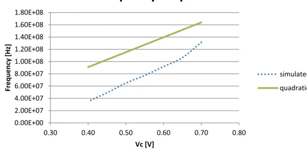
stage ring VCO in UMC130 technology, the proposed model yields the frequency response
represented in figure 2.5. The results obtained when compared to those obtained from simulating
with Spectre simulator lead us to the conclusion that the proposed model, which relies on the
12 0.00E+00 2.00E+07 4.00E+07 6.00E+07 8.00E+07 1.00E+08 1.20E+08 1.40E+08 1.60E+08 1.80E+08
0.30 0.40 0.50 0.60 0.70 0.80
Frequ enc y [H z] Vc [V]
Frequency Response
simulated quadraticThus, a new model should be used, relying on a transistor level, accurate for sub-micron
technologies.
In this work, the EKV model was used in order to overcome this inaccuracy. The EKV model is a
compact model which provides continuity of the large and small signal characteristics from weak
to strong inversion, once a unique parameter describes the behavior in all operating regions trough
precise and simple equations. Also one of the strengths of this model relies on the use of one
expression for modeling the drain current, capable to cover all inversion charges with a good
precision for both weak and strong inversion[10-12]. Thus, the drain current is given by:
( ) (2.9)
Where and are the forward and reverse currents, which can be obtained through:
( ) [ ( [ ( )])] (2.10)
And the specific current is defined as:
(2.11)
13 Thus, the frequency of oscillation turns into:
( )
(2.12)
To validate the accuracy of the EKV model and compare it against the one based on the quadratic
law for the transistor current, a seven stage with symmetrical differential load Ring VCO will be
14
2.4.
Working Example and Results
In order to verify the accuracy of the EKV model, a seven stage symmetrical differential load
Ring VCO was considered, where each delay cell has the configuration presented in Fig. 2.5. The
transistors sizes are shown in the following table.
Table 2.1- Transistor Sizes for the working example
Load (Pmos) Switch (Nmos) Bias (Nmos) W L
This working example was considered without load capacitance. For the evaluation of the
effective capacitance , the following approximation, explained further in this work, was used
( ) (2.13)
The achieved results for this proposed VCO model are illustrated in the Fig.2.6.
Figure 2.6- Frequency Response of the VCO
0.00E+00 2.00E+07 4.00E+07 6.00E+07 8.00E+07 1.00E+08 1.20E+08 1.40E+08 1.60E+08 1.80E+08
0.30 0.40 0.50 0.60 0.70 0.80
15 From the Fig.2.6 it is easy to conclude that when sub-micron technologies are used, the model
based on the quadratic law for the transistor current presents quite inaccurate results. It is also
possible to observe the accuracy of the results with the EKV model, where the majority of the
points along the curve have relative errors inferiors to 7%.
2.5.
Conclusions
In this chapter a brief introduction to VCO for RF applications was given. The particular case for
differential Ring VCOs with the Maneatis delay cell was presented and the corresponding models
proposed in the literature were presented. The necessity for having accurate models for the
automatic design of Ring VCOS was pointed out. Finally the limitations of the proposed models
for VCOs in deep submicron technologies were illustrated through a working example
considering a seven-stage ring oscillator. Since the inaccuracy of the results obtained with the
models presented stems from the inadequacy of using the MOS quadratic model to characterize
the transistors with submicron sizes, the EKV model was briefly introduced and its application for
the development of the ring VCO model was proposed. Results with this new model, for the
working example considered, prove the adequacy of this new model.
Further in this work, a more profound analysis on the design of a Ring VCO with symmetrical
load and its limitations will be made, as well as a more profound approach to the EKV model and
17
3.
EKV Models
3.1.
Introduction
This chapter is dedicated to the use of the EKV Mosfet model for the characterization of
transistors in deep-submicron technologies. After introducing the EKV model a detailed
description of the methodology adopted for the determination of the EKV model parameters for
the UMC130 technology is given. For the automatic determination of the EKV model parameters
a script in Matlab was developed.
Finally, the validation of the model parameters obtained is accomplished through the
determination of the delay introduced by single inverter stages with the EKV model. The
validation is accomplished through the comparison against results obtained from simulation with
Cadence Spectre.
3.2.
The EKV Model
The EKV Model is a charge-based physical model dedicated to the design and analysis of
low-voltage and low-current circuits, built on fundamental physical properties of the MOS structure.
This compact model provides continuity of the large and small signal characteristics from weak to
strong inversion, once a unique parameter set (“This model has only 9 physical parameters, 3 fine
tuning fitting coefficients, and 2 additional temperature parameters [11].”) describes the behavior
in all operating regions and over all device geometries with great accuracy.
The model respects and preserves the inherent symmetry of the device by referring all the
voltages, the drain voltage , the source voltage and the gate voltage , to the local substrate
(bulk), as depicted in Fig. 3.1[12]:
| | (3.1)
| | (3.2)
18
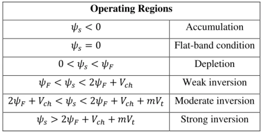
The transistor operating regions can be described through the surface potential defined as the
electrostatic potential at the semiconductor surface, the Fermi potential as the quasi-Fermi
potential of the majority carriers and the channel potential which depends on the position along the channel and is defined as the difference between the quasi-Fermi potentials of majority
and minority carriers along the channel. This channel potential represents the disequilibrium in
electron distribution produced by the source and the drain voltages. The description of the
different operating regions can be found in the Table 3.1[12].
Table 3.1- Operating Regions of a EKV transistor, with respect to the surface potential
Operating Regions
Accumulation
Flat-band condition
Depletion
Weak inversion
Moderate inversion Strong inversion
In the inversion region, and thus the mobile inversion charge density , which can be defined as a function of and by integrating Poisson’s equation, converts to[11, 12]:
√ [√ ( ) √ ] (3.4)
The gate voltage can be obtained through the surface potential and the mobile inversion
charge density by applying:
19 √
(3.5)
Where is the flat-band voltage, is the gate-oxide capacitance obtained through the relation between the dielectric constant and the oxide thickness , and the body effect , which depends on the substrate doping concentration , given by:
√
(3.6)
In strong inversion the surface potential can be written as:
(3.7a)
Where
(3.7b)
Thus, expressing the inversion charge as a function of and using the Eqn. 3.5 will result:
[ ( )] (3.8)
Where is the gate threshold voltage referred to the local substrate and defined as:
[√ √ ] (3.9)
The threshold voltage is defined as the gate voltage such as when the channel is at equilibrium ( ), and follows:
| | √ (3.10)
The pinch-off voltage is a channel potential for which, at given gate voltage, the inversion
charge becomes zero, as stated in [x]. Hence
| | √ √ (3.11)
The latter equation can be expressed in terms of the gate voltage by simply inverting Eqn. 3.11:
20
The value of can also be determined by the value of corresponding to the point where the pinch-off voltage is zero
(
). The derivative of the gate voltage
with respect to the pinch-off voltage is defines as the
slope factor n
and is given by:
√ (3.13)
The pinch-off voltage and the slope factor as functions of the gate voltage are depicted in Fig.3.2:
By applying the definition of the pinch-off voltage into Eqn. 3.8, the inversion charge results:
[ (√ ) √ ] (3.14)
It is possible to deduce that the pinch-off voltage can be interpreted as the equivalent effect of the
gate voltage referred to the channel.
21
3.2.1.
Weak inversion
The inversion charge decreases smoothly down to zero as the channel leaves strong inversion.
When the channel voltage becomes smaller than the pinch-off voltage , the channel is in weak inversion and the inversion charge becomes negligible with respect to the depletion charge.
Hence, introducing the definition of , the gate voltage becomes[11, 12]:
( ) (√ √ ) (3.15)
Although has been defined in strong inversion operation, it can also be used in weak inversion
to approximate the surface potential. Comparing the Eqn. 3.15 and Eqn. 3.11, the surface potential
can be obtained by applying:
(3.16)
By introducing the result in the solution of the Poisson equation in (3.4) and applying the Taylor
expansion, the inversion charge in weak inversion can be approximated to a simplified
expression:
( ) ( ) ( ) (3.16)
3.2.2.
Drain Current
The drain current is obtained by integrating the inversion charge along the channel, from the
source ( ) to the drain ( ), assuming constant mobility along the channel:
∫
(3.17)
Where:
22
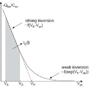
The inversion charge as a function of the channel potential is illustrated in Fig. 3.3. Since the
drain current is determined by integration of the inversion charge along the channel potential, it is
proportional to the shaded surface comprised between the source and the drain voltage. The
integral can be rewritten by decomposing into a forward current and a reverse current
defined by[10-12]:
∫
∫
(3.19)
The forward current corresponds to area delimited by the difference , while the reverse
current corresponds to the area delimited by the difference . It is possible to conclude that
when the drain voltage is increased, the area corresponding to the difference is
reduced and therefore the reverse current is reduced. The forward saturation is attained when the
drain voltage reaches the pinch-off voltage , which will make the channel to pinched-off at the
drain and the reverse current becomes zero ( ). Thus, in forward saturation the drain current
becomes equal to the forward component of the current . Another conclusion possible to extract
from the figure, is the fact that the inversion charge is an exponential function of , in weak inversion, which results in an exponential forward(reverse) current ( ):
( ) [ ( )] (3.20)
23 Where is defined as the specific current given by:
(3.21)
The specific current characterizes the drain current when the transistor operates in the center of
moderate inversion, and depends on technology and transistor geometry. Thus the specific current
plays an important role as design parameter that helps sizing the transistor to an imposed bias
current and a given mode of operation.
Making use of the approximations for the inversion charge presented above in this chapter, it is
possible to obtain the expressions for the forward and reverse currents for both weak and strong
inversion. Since, it is important to determine one expression capable to cover all inversion charges
with a good precision, mathematical interpolation is applied yielding, the expression valid for all
the different inversions is given by:
( ) [ ( [ ( )])] (3.22)
Finally, the drain current is given by:
( ) (3.23)
The parameter extraction methodology along with the model validation will be presented in the
24
3.3.
Parameters Extraction
This section describes the parameter extraction methodology, as well as the results obtained and
their validation.
3.3.1.
Drain Current
As already mentioned in the presentation of the EKV model, the drain current is decomposed in a
forward and reverse current and , combined in a single expression for linear and saturation
regimes and valid from weak to strong inversion. These currents are functions of and
respectively:
( ) ( ) (3.24)
The expression for the drain current can be obtained applying a normalization factor called
specific current :
( ) [ ( [ ( )])] (3.25)
Where is obtained through a parameter extraction and ⁄ .
3.3.2.
Extraction of
In the MOS transistor saturation region, the reverse current approaches zero and so becomes
negligible with respect to forward current . Therefore, the drain to source current can be
approximated by[13]:
[ ( [ ])] (3.26)
In saturation [
] , yielding
25 Hence
(√ ) √
( ) (3.28)
And thus
(3.29)
Given (3.28), the can be extracted by applying a fixed gate voltage and determine the
strong inversion slope of the √ characteristic[13, 14]. To find the value of the slope, a
fitting of the characteristic obtained in simulation with a straight line was applied, using the
optimization tool available in Matlab.
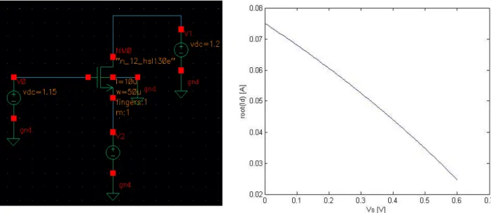
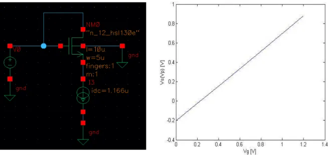
A configuration of the circuit used to measure the , as well as the simulation result, are illustrated in the figure 3.4a and 3.4b respectively.
26
3.3.3.
The Pinch-off Voltage
The pinch-off voltage corresponds to the value of the channel potential for which the
inversion charge density extrapolated from strong inversion becomes zero[13, 14].
[√ ( ) ]
(3.30)
√ (3.31)
Where is the threshold voltage defined as the gate voltage for which the inversion charge forming the channel is zero at the equilibrium ( ), is the approximation of the surface
potential in strong inversion and is the body effect and given by
√ ⁄ (3.32)
These parameters can be extracted through a fitting of the characteristic, using the circuit
configuration presented in Fig. 3.5a. Note that, in this configuration, the value of the current
source must be half of the specific current. The characteristic obtained in the simulation is
illustrated in Fig.3.5b.
27
Through this measures it’s also possible to obtain the weak inversion slope factor , defined as
the inverse of the partial derivative of the pinch-off voltage with respect to the gate voltage, and
so:
[ ] (
√ )
(3.33)
Once found the slope factor , the value for the parameter can be obtained through:
(3.34)
Although, it is needed to acquire the mobility reduction coefficient . This parameter can be
achieved through a fitting of the versus characteristic using the same circuit configuration,
since: (3.35) In saturation, ( ) (3.36) Thus, (3.37)
Also notice that the approximation it is just valid for large devices, otherwise the correct
body effect fact has to be taken into account.
This way depends on the effective channel length and width, as well as on the drain and source
voltages and , due to coefficients for short-channel and for small-channel
effects, through the following expression[14]:
[ √ (
28
The pinch-off voltage extraction consists in using a constant current bias, typically equal to half of
the specific current as mentioned before, to measure the versus characteristic in moderate
inversion by sweeping the gate voltage and measuring the source voltage .
As it was said above, is determined by a certain value of corresponding to the point where crosses zero ( ), being the unique parameter without need of extrapolation. The parameters and are extracted by fitting (3.30) to the measured
characteristic. In the figure 3.6 can be found the results of this extraction as well as it correctness,
where the straight line is the characteristic measured and the symbol plus is the characteristic
achieved by applying the values of the parameters.
Once these parameters for large devices are obtained, the parameters and can be
extracted from the measured pinch-off voltage characteristic (short-channel and narrow-channel
respectively) by fitting (3.38) but taking into account the correct body effect. Note that in the
extraction of LETA, thus for a device with a short-channel length, the coefficient WETA is
neglected, and vice-versa. This way, the accuracy of the results for this extraction is founded on
the figure 3.7, where it is possible to observe the characteristic measured as well as the
characteristic achieved using the obtained values for the transistor PMOS.
Figure 3.6- Estimated vs Simulated results from Vp vs Vg characteristic. Nmos: W=50u, L=10u. Pmos: W=10u, L=1u
29 Finally, the parameters values obtained for both NMOS and PMOS transistors are presented in the
following tables.
Table 3.2 Nmos transistor Parameters
NMOS
( ) (V)
2,33 0,1875 0,209 0,7234 0,002 0,344 0,0351 0,9765
Table 3.3 Pmos transistor Parameters
PMOS
( ) (V)
1,63 0,2508 0,4594 1,4088 9,65E-4 0,0869 0,0083 0,25
In order to check the accuracy of the parameters extracted, the ( ) characteristic obtained with the EKV model was compared against simulation results as presented in the Fig. 3.8.
From the Fig. 3.8, it is possible to consider that the results are quite acceptable and thus the values
for the parameters valid.
For validating the results obtained in all regions of operation of the MOS transistor, the transient
30
3.3.4. Automatic Generation of the EKV Model Parameters
For the automatic generation of the EKV model parameters a script was developed in Matlab. The
source code for this script can be found in Annex I.
The script developed starts by considering the DC simulation response from the circuit
represented in figure 3.4. From these results, the square root of the drain current values for each
source voltage is evaluated and the value for the specific current is obtained.
Once obtained the specific current , the script considers the DC simulation of the circuit with the
configuration presented in figure 3.5. From these results, the values of and are considered in
an optimization tool provided by Matlab, to fit the data obtained to the expression for the
pinch-of-voltage represented by the equation (3.30), and the values for the parameters and are
obtained. Through the estimation of the values of the pinch-of-voltage, the weak inversion slope
factor using the equation (3.33) it is obtained.
For the evaluation of the parameter , the script considers the DC simulation of the circuit
with the same configuration as in figure 3.5, although with a smaller value for the width of the
transistor. From the results obtained, the pinch-of-voltage is evaluated in order to obtain the
values for the correct body effect through the equation (3.30). The next step, where the
parameter is obtained, is to introduce again in the optimization tool the results obtained
from the evaluation of the correct body effect to fit into the expression (3.38) considering
. The inverse procedure is considered for the evaluation of the parameter .
Finally, the script considers again the DC simulation response from the circuit represented in
figure 3.5. From these results, the values of the drain current are introduced in the optimization
tool for a fitting to the equation (3.7) and the value for the parameter related to the mobility
reduction coefficient is obtained. After the evaluation of the parameter , the parameter is
31
3.4.
Work Examples
3.4.1.
Single Inverter
Extracted all the EKV model parameters needed for the study and carried out its verification and
validation, a Matlab prototype was built, with functions based on the model equations, in order
efficiently study the behavior of the transistor for different circuits topologies. With the interest of
verifying the model accuracy, a comparison was made on the behavior of an inverter in a Cadence
simulation against the behavior obtained through the model designed.
The results obtained were quite satisfactory, since the output curves of the model match with the
output curves obtained through simulation as it is possible to observe in figure 3.9, where the
straight line corresponds to the output estimated and the symbol plus correspond to the output
simulated.
32
3.4.2.
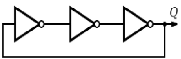
Three Stages Inverter
In a second example, the circuit with three inverters represented in Fig. 3.9 was considered. This
topology was adopted in order to check the delay between stages.
From the Fig. 3.10 below, it is possible to conclude that the model designed presents the expected
behavior. The output obtained from the model is an excellent approximation to the one obtained
from the simulation.
The values of the delays between stages as well as the respective relative errors are presented in
the following Table 3.4.
Figure 3.10- Three Stage Inverter Configuration. Nmos: W=20u, L=5u. Pmos: W=80u, L=10u
33
Table 3.4 Model vs Simulation delays and relative error
Delay Matlab Delay Cadence Relative Error [%]
Stage 1 to 2 1,91E-07 Stage 1 to 2 2,04E-07 -6,53
Stage 1 to 3 3,13E-07 Stage 1 to 3 3,24E-07 -3,42
Stage 2 to 3 1,22E-07 Stage 2 to 3 1,20E-07 1,87
The relative errors may be due to the fact that the model does not consider yet the parasite
capacitances of each transistor. However the results were quite accurate since the highest relative
error is inferior to 7%.
From the results obtained with the working examples described above, it is possible to conclude
that the parameters extracted present a good accuracy making the model valid.
3.5.
Conclusions
In this chapter an introduction to EKV Mosfet model was given. The methodology adopted for the
evaluation of the EKV model parameters was carefully described. A Matlab script for evaluating
the EKV model parameters for both NMOs and PMOs transistors was developed and the results
obtained for UMC130 technology transistors were presented. The validity of the parameters
obtained was carried out through comparison with simulation results with Cadence, for the
determination of ID(vgs) characteristics of both NMOs and PMOs transistors. Finally working
examples considering the generation of the output characteristic of a switching inverter and the
determination of delays for a chain of inverters were considered. The accuracy of results, checked
against simulation with Cadence Spectre is demonstrated.
These results lead us to the conclusion that the EKV model is adequate for the characterization of
symmetrical-load ring VCOs. In the next chapter, the application of the EKV model for the
characterization of Ring-VCOs and further application to the optimization-based design of VCOs
35
4.
Project of a VCO with EKV Model
4.1.
Introduction
This Chapter addresses the optimization-based design of Nmos symmetric load ring VCOs. After
a brief introduction to optimization-based design methodologies, the new model for characterizing
the NMOs symmetric Load Ring VCO in submicron technologies will be presented. The validity
of the VCO model for UMC130 Technology will be checked against simulation results. Finally,
working examples considering the optimization based design of ring VCOs for oscillation
frequencies up to 1.7 GHz will be presented.
4.2.
Ring VCO Design Considerations
The design of analog blocks is usually performed through an iterative process. Designers start
with a first solution based on very simple models and then, using heuristic rules altogether with
electrical simulation, in an iterative procedure, perform the tuning of the design solution fitting to
the envisaged specifications. During the last years, the necessity for designing analog/RF building
blocks with ever more stringent specifications that push the circuits to the limits of the feasibility
allowed by the technologies makes the use of optimization methodologies more popular[1, 6, 9].
Regarding optimization two different approaches may be considered. In a first methodology, that
mimics the analog design previously described, the electrical simulator is integrated into an
optimization engine. Sometimes, dedicated tools are developed which also allow the inclusion of
heuristics into the optimization loop. In the particular case for ring VCOs this electrical
simulation based optimization approach is not an efficient solution, since the characterization of
VCOs is accomplished through lengthy transient simulations. In this case, the optimization
should be performed using an accurate and not very complex VCO model.
In chapter 2 a simple and accurate model for evaluating the oscillation frequency of an NMOs
symmetric load ring VCO was proposed. The accuracy of the model, when applied to submicron
technologies is granted through the use of the EKV transistor model.
Yet for introducing this model into an optimization loop it is fundamental to understand the
36
validity limits, we will be restricting the design space and a more efficient optimization is
attained.
Furthermore, an evaluation of the design trade-offs will help understand the key factors in the
design process.
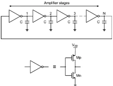
In the next subsections some considerations regarding the qualitative influence of the several
elements comprising the Maneatis cell, as illustrated in Fig. 4.1, will be studied.
In the Fig. 4.1 is presented the configuration of the Maneatis cell, where the red section
corresponds to the symmetric load cell while the green section represents the transistors
responsible for the switching, as well as the bias current source. The current source used grants an
oscillator output signal swing equal to the control voltage Vc. For the model to be valid, we must
guarantee that the biasing current source remains in the saturation region, and that the switching
transistors may be approximated to ideal switches. These considerations raise a limit to the maximum value of Vc that prevents both the biasing and the switching transistors to enter triode
region of operation.
𝑀
𝑆𝐿𝑀
𝑆𝐿𝑀
𝑆𝐿𝑀
𝑆𝐿𝑀
𝑆𝑊𝑀
𝑆𝑊𝑀
𝐶𝑆𝑀
𝑆𝑊𝑀
𝐶𝑆𝑀
𝑆𝐿𝑀
𝑆𝐿37 Through the inspection of the proposed model, Eq. (2.12) we may conclude that the frequency of
oscillation depends, fundamentally on the current provided by the bias stage and on the load
capacitance.
In the next subsection the influence of each of these elements will be studied.
4.2.1.
Bias Stage
A first analysis on the influence of the bias transistors size is evaluated. As it was already said, the
current source of the Maneatis cell is designed such that the output voltage swing is equal to the control voltage . In order to understand its influence, a simulation was made for different
sizes of the bias transistors, for an oscillator with seven stages.
In the 0.00E+00 1.00E+07 2.00E+07 3.00E+07 4.00E+07 5.00E+07 6.00E+07 7.00E+07
0.35 0.45 0.55 0.65 0.75
Frequ enc y [H z] Vc [V]
Frequency vs Vc
Cadence(Wb/Lb=30/2)
Matlab
Cadence(Wb/Lb=30)
Cadence (Wb/Lb=100/0.5)
38
In the Fig.4.2 above is presented the Frequency vs Vc characteristic of the ring oscillator with 7
stages obtained through the Cadence simulations against the characteristic estimated through the
Matlab simulation. Since the model implemented in Matlab does not take into account the bias
transistor sizes, only one response is obtained. There are several conclusions possible to extract
from this chart.
The first point relies on the difference between the frequency values of the Cadence simulations
against the one from Matlab. In this case a load capacitance of 2F was used as a way of using an
approximate model that does not take into account the mosfet capacitances. This approximation
may justify the difference between the simulated and the results obtained with the matlab model.
Another analysis possible to extract, relies on the influence of the W/L ratio of the bias stage
transistors. It is possible to observe that for higher values of W/L, the curve approximates to a
linear function (for a control voltage not exceeding the boundaries of , otherwise
the bias stage will not work properly), and to values similar from the ones estimated in Matlab.
The latter happens due to the increase of the current with the W/L ratio, which will make the bias
transistor maintain the saturation for lower values of .
In the next sub-section, an analysis on the approach used to calculate the effective capacitance of
the oscillator will be presented since it will have a direct influence on the output frequency and
thus on the design of the switch and load transistors.
4.2.2.
Effective Capacitance
With the purpose of taking into consideration, in the model designed in Matlab, the parasitic
capacitances of the transistor, a study was carried out in order to check the accuracy of the results
using the following approximation for the effective capacitance[6]:
( ) (4.1)
For the development of this study, several simulations were made with the oscillator composed by
3, 5 and 7 stages without load capacitance and changing the size of the switch and the load
transistors. The value of the effective capacitance of the oscillator was obtained through the
39
(4.2)
And thus,
(4.3)
Once obtained the results of the different simulations, a comparison was made between the values
of the effective capacitance of the simulation and the ones estimated by the model, presented in
the Table 4.1 below. Notice that the values presented were obtained for a 7 stages oscillator, using
a control voltage of 0.6V for the simulations and for the estimation of the equivalent
capacitance in the model.
Table 4.1- Capacitance simulated vs Capacitance estimated
[ ] [ ] [ ]
21,3µ 0,5µ 10µ 0,33µ 0,211 0,198 6,94
42,6µ 0,5µ 10µ 0,33µ 0,106 0,112 -6,18
42,6µ 0,5µ 20µ 0,66µ 0,283 0,28 1,29
42,6µ 0,5µ 30µ 0,66µ 0,309 0,335 -7,61
42,6µ 0,5µ 40µ 0,66µ 0,341 0,39 -12,58
It is also important to observe the influence of this approach in the values estimated for the
frequency of oscillation when compared to the values of the simulation. This way, a comparison
is made between the frequency values of the simulation and the estimated ones, for the same size
of the transistors, as presented in the following table 4.2.
Table 4.2 Frequency simulated vs Frequency estimated
[ ] [ ] [ ]
21,3µ 0,5µ 10µ 0,33µ 0,451 0,504 -10,53
42,6µ 0,5µ 10µ 0,33µ 0,451 0,442 2,20
42,6µ 0,5µ 20µ 0,66µ 0,336 0,355 -5,39
42,6µ 0,5µ 30µ 0,66µ 0,308 0,297 3,68
40
It is possible to observe that the approach for the equivalent capacitance used in the model,
presents accurate results, with relative errors inferiors to 10% for most of the cases. Allowing to
conclude that the approach presented above is a valid approximation.
By analyzing Eqns. (4.1) and (4.2) it is possible to conclude that a careful choice of the size of the
load and switch transistors must be made. From one hand, increasing the size of the load
transistors will increase the current along with the output frequency. Although, increasing the size
of the load transistors will also increase the effective capacitance, which will decrease the
frequency. The same balance happens with the switch transistors. From one side, increasing the
size of the switch transistors will increase their speed of commuting. Although, increasing the size
of the switch transistors will also increase the effective capacitance. Therefore, this balance has to
be taken into account when sizing the load and switch transistors.
The existence of the above mentioned trade-offs among the several transistor sizes, leads to the
conclusion that the design of Ring-VCOs is a good candidate for optimization based design.
In the next sub-section, several examples resulting from the optimization based design of
41
4.3.
Optimization of Ring VCOs
Once the model is fully designed and validated, it was included in an optimization-based script
developed for the automatic design Ring VCO. This script enables the designer to obtain the
transistors sizes for the delay cell of the ring VCO, for predefined values for the number of delay
stages and the envisaged oscillation central frequency. The source for this script is included in
Annex II. For the evaluation of the frequency vs control voltage characteristic, the equation (2.12)
is used. For the evaluation of the currents, the EKV model with the parameters described in
Chapter 3 were used. The evaluation of the effective Capacitance is obtained with (4.1).
The optimization of the oscillator consists in choosing a certain value of frequency, and fixing 2
of the 4 variables related to the length and width of both load and switch transistors. Notice that
the sizes of the transistors were obtained for the central frequency with a control voltage of 0.6V.
It is also clear, from Eqn. (4.2) that the frequency of operation cannot be the same for oscillators
with 3, 5 and 7 stages. Thus, increasing the number of stages will limit the value of the maximum
frequency possible to attain.
In the work example presented in this section, the sizes of the transistors were obtained for a
frequency of operation of for oscillators with 7 and 5 stages, and for a 3 stage
oscillator. The results of the optimization for these values of frequency concerning the size of the
transistors are presented in the following Table 4.3.
Table 4.3 Transistors sizes optimization
[ ]
3 30,2µ 0,39µ 78,9µ 0,39µ 1
5 57,9µ 0,39µ 63,6µ 0,66µ 0,5
7 80,0µ 0,39µ 71,4µ 0,40µ 0,5
Given the sizes of the transistors for each cell in each oscillator, a comparison was made between
the values obtained from simulation against and the ones estimated from the model, concerning
the frequency output, for a range of values for the control voltage between .
The acquired results and its respective relative errors, related to the different oscillators, are
42
Table 4.4- Frequency estimated against frequency simulated for a 7 stage Ring VCO
[ ] [ ] [ ] [ ]
7
0,4 0,887 0,818 -7,85
0,45 0,790 0,708 -10,34
0,5 0,693 0,638 -7,87
0,55 0,595 0,589 -1,05
0,6 0,499 0,498 -0,21
0,65 0,405 0,422 4,31
0,7 0,314 0,344 9,74
Table 4.5- Frequency estimated against frequency simulated for a 5 stage Ring VCO
[ ] [ ] [ ] [ ]
5
0,4 0,89 0,785 -11,81
0,45 0,792 0,720 -9,06
0,5 0,694 0,663 -4,53
0,55 0,597 0,585 -2,14
0,6 0,50 0,511 2,14
0,65 0,405 0,437 7,83
0,7 0,315 0,357 13,55
Table 4.6- Frequency estimated against frequency simulated for a 3 stage Ring VCO
[ ] [ ] [ ] [ ]
3
0,4 1,78 1,72 -3,28
0,45 1,58 1,55 -1,91
0,5 1,39 1,39 0,09
0,55 1,19 1,21 1,32
0,6 1,00 1,03 2,78
0,65 8,11 8,53 5,16
0,7 6,29 6,72 6,89
From the presented results, there are several conclusions possible to extract. The first conclusion
relies on the small values for the relative errors, where the average error is inferior to 7%, making
43 From the analysis of the results, it is also possible to observe that the relative error increases as
the limits of the range of the control voltage are reached. The latter can be explained by the fact
that the oscillator was designed with a value for the control voltage of , and by the fact that
for values of the control voltage higher or lower than the range presented, the bias stage will not
work properly.
Finally, as expected from Eqn. 4.2, the value of the operation frequency increases with the
decrease of the control voltage and vice-versa.
![Figure 2.4- Maneatis d symmetric load delay cell [1]](https://thumb-eu.123doks.com/thumbv2/123dok_br/16570591.737990/27.892.309.591.800.1075/figure-maneatis-d-symmetric-load-delay-cell.webp)
![Figure 2.6- Frequency Response of the VCO 0.00E+002.00E+074.00E+076.00E+078.00E+071.00E+081.20E+081.40E+081.60E+081.80E+080.300.40 0.50 0.60 0.70 0.80Frequency [Hz]Vc [V] Frequency Response simulatedekvquadratic](https://thumb-eu.123doks.com/thumbv2/123dok_br/16570591.737990/32.892.126.741.644.1016/figure-frequency-response-vco-frequency-frequency-response-simulatedekvquadratic.webp)