Sabrina Josephine Rubin
Licenciada em Engenharia de Micro e Nanotecnologias
Development of eco-friendly ZnO inks for
paper-based printed electronics
Dissertação para obtenção do Grau de Mestre em
Engenharia de Micro e Nanotecnologias
Orientador: Doutor Luís Miguel Nunes Pereira, Professor Auxiliar, Fa-culdade de Ciências e Tecnologia da Universidade Nova de Lisboa
Júri
Presidente: Doutor Rodrigo Ferrão de Paiva Martins Arguente: Doutora Marja Vilkman
Development of eco-friendly ZnO inks for paper-based printed electronics
Copyright © Sabrina Josephine Rubin, Faculdade de Ciências e Tecnologia, Universidade NOVA de Lisboa.
Ac k n o w l e d g e m e n t s
After all the effort made these past months, including frustrating results, sometimes
days spent on one single detail, but also memorable and exciting moments, this master thesis would not have been possible without the help and guidance of a large number of people.
I would like to thank Prof. Elvira Fortunato and Prof. Rodrigo Martins for the priv-ilege and opportunity to work at the prestigious CENIMAT|i3N and CEMOP. The fully equipped laboratories, expertise and passion for science as well as the positive demand for innovative and challenging work all create the excellent conditions and scientific basis for this thesis and other works.
Secondly, I would like to express my sincere gratitude to my supervisor, Prof. Luís Pereira, for accepting me into the team, for all the suggestions, weekly meetings, help and ideas, all contributing to the excellent team spirit.
To Inês Cunha, my co-supervisor, partner to all the endless lab work, humorous mo-ments, serious and frustrating moments and most valuable suggestions and help, from the very basic problems to the head-scratching complicated problems. Her persistence, knowledge, ideas, never-ending energy, trust in my work, mini pep-talks (all the time spent helping me!) and constantly pushing me to better results helped to surpass many difficulties encountered in this work. The vital electrolyte component used in this work
and opportunity to freely cut and use (almost all!) her ion gel for the countless transistors will not go unnoticed. Thank you! Besides co-supervisor, you are a great friend.
I am also grateful for all the support given by the extraordinary group of researchers which include Rogério Morais, Tiago Carvalho, Raquel Barras, Paul Grey, Emanuel Carlos, Gabriel and Ribas. Thank you guys for all the tips, knowledge, inspiring long hours of work spent at Lab 5, 6 and 7, the laughs and never ending patience with me. To Rogério, for showing me the basics at the printing lab. To Tiago and Raquel for helping me with the equipment and expertise and sharing weird and funny moments. To Paul and Manu, for the circuit knowledge and wise advice at the electrical characterization workbench. Gabriel and Ribas, you guys kept the environment uplifting and solidarity.
To my colleagues working with me at CENIMAT, there has never been a quieter and hilarious OpenSpace to work at.
To all my course colleagues, a big thank you. I would not have come so far alone, all of your support and help I will keep with me forever. Marta, I have never had a better friend for head-banging on the walls. You also belong above in the team paragraph, but are most of all my course friend. Miguel, thank you for the advice all the way from Braga. Fernocas (your nickname forever) from Braga, even though I never see you, thank you for the friendship since the 1st year. To Catarina, for the unconditional support even all the way from Japan. Caupi, for wise words from Finland. Cláudia, you also belong to the international paragraph, thank you for the support from England.
To my whole family, for the unconditional support, love and comprehension, that words cannot express. To my parents, for showing me in a real-life example, that even after five times, even the impossible becomes possible and you should never ever give up. To my brothers, for putting up with your annoying sister, "let’s go to the beach", "come on hurry up let’s watch a movie", 9gag posts, memes, fail videos, Praia da Rocha moments, making fun of absolutely anyone and anything and making me laugh when I’m trying to stay mad.
To Ricardo, thank you for being the light on dark days, for the incomprehensible patience with me, keeping me strong during this stressful period and making me laugh when I thought it impossible. Also for "está na hora", guitarradas with the bros, film sessions, all the trips, Algarviadas, pep talks and reminding me of what is the most important.
A b s t r a c t
In this work, we report the development of printable semiconducting inks compatible with screen-printing and paper technology and functional at room temperature without the need of post-deposition treatments. The developed eco-friendly inks are based on a dispersion of zinc oxide nanoparticles on a cellulose matrix. Several cellulose derivatives were used to design and engineer such inks looking for the best formulation, printing conditions and compatibility with cellulose-based substrates. The approach described here represents an innovative and versatile generation of semiconducting inks composed of some of the cheapest, renewable and highly abundant materials we can find on Earth, such as cellulose, able to be implemented as channel in printed transistors on paper.
By using a cellulose-based ion gel as gate dielectric the printed ZnO transistors exhibit an Ion/of f ratio ranging from 103 to 105, µ
sat values close to 9 cm2 V−1 s−1 andgm of
around 0.4 mS.
R e s u m o
Neste trabalho, reportamos o desenvolvimento de tintas semicondutoras de impres-são compatíveis com screen-printinge tecnologia de papel e funcionais à temperatura
ambiente sem a necessidade de tratamentos de pós-deposição. As tintaseco-friendly de-senvolvidas baseiam-se numa dispersão de nanopartículas de óxido de zinco numa matriz de celulose. Vários derivados de celulose foram usados para projetar estas tintas, procu-rando pela melhor formulação, condições de impressão e compatibilidade com substratos baseados em celulose. A abordagem descrita aqui representa uma geração inovadora e versátil de tintas semicondutoras compostas por alguns dos materiais mais baratos, reno-váveis e altamente abundantes que se podem encontrar na Terra, como a celulose, que podem ser implementados como canal em transistores impressos em papel.
Ao utilizar um gel iónico à base de celulose como dielétrico de porta, os transistors de ZnO impressos exibem um rácio deIon/of f entre 103e 105, valores deµsat pertos de 9
cm2V−1s−1e umg
mde 0.4 mS.
Palavras-chave: Óxido de zinco, transístor de porta eletrolítica, eletrónica impressa,
L i s t o f F i g u r e s
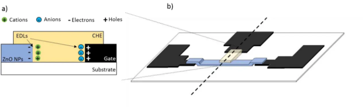
2.1 a) Cross-section schematic representation of the EDL formations at each inter-face. b) A 3D schematic representation, where the white substrate represents paper, three black contacts representing carbon electrodes (the dashed line goes through the gate electrode), blue layer as the ZnO NPs layer and the
topmost layer between gate and ZnO NPs layer as the CHE sticker. . . 8
2.2 Schematic drawing of custom-made screen-printing system used at CENI-MAT|i3N. [25] . . . 10
4.1 TG-DSC curves of Z40C3 ink. . . 18
4.2 TG-DSC curves of Z40H5 ink. . . 19
4.3 FTIR spectra of Z40C3 for three temperatures, 25, 60 and 120 °C. . . 20
4.4 FTIR spectra of Z40C3 for 25 °C varying with time. . . 21
4.5 FTIR spectra of Z40C3 for 60 °C varying with time. . . 21
4.6 FTIR spectra of Z40C3 for 120 °C varying with time. . . 22
4.7 SEM images of Z40C3 ink printed on different substrates, from left to right, office paper, tracing paper and FS2 paper. . . 23
4.8 SEM images of Z40H5 ink printed on different substrates, from left to right, office paper, tracing paper and FS2 paper. . . 23
4.9 SEM images of Z40H15 ink printed on different substrates, from left to right, office paper, tracing paper and FS2 paper. . . 23
4.10 XRD diffractogram of CMC powder and Z40C3.. . . 24
4.11 XRD diffractogram of HPC powder and Z40H5. . . 24
4.12 Influence of the formulation of the semiconducting inks, dried at room tem-perature, on the transfer curves: polymer concentration (top) and ZnO NPs concentration (bottom). . . 26
4.13 Transfer curves of Z40C3 printed on office paper, comparing up to 5 semicon-ductor layers.. . . 28
4.14 Aspect of printed semiconductor film for Z40C3, on office paper. . . . . 29
4.15 Transfer curves of printed ZnO EGTs on office paper and annealed at 25, 60 and 120 °C, showing three samples for each temperature. . . 29
L i s t o f Fi g u r e s
4.17 Comparison of transfer curves from the three best formulations considering three cellulose derivatives. . . 31
4.18 Comparison of transfer curves from the three best formulations considering three cellulose derivatives, showing each leakage current. . . 32
I.1 Amplification of patterned electrodes showing the width (W) and length (L) of the channel. . . 39
II.1 TG-DSC curves of the ZnO NPs inks. Top, from left to right: Z40C3, Z50C3 and Z40C5. Bottom, left to right: Z40H5, Z40H10 and Z40H15. . . 41
L i s t o f Ta b l e s
3.1 Table summarizing all developed inks with a nomenclature for each formula-tion. . . 14
4.1 Electrical parameters of the EGTs considering CMC and HPC . . . 26
4.2 Electrical parameters of ZnO NPs ink printed on office paper, comparing up
to 5 semiconductor layers. . . 28
4.3 Electrical parameters of printed ZnO EGTs on office paper and annealed at 25,
60 and 120 °C. . . 29
4.4 Electrical parameters of printed ZnO EGTs using Z40C3 on office paper, FS2
paper and tracing paper. . . 30
4.5 Electrical parameters of the printed ZnO EGTs on office paper considering
three samples for each of the three formulations. . . 31
Ac r o n y m s
a.u Arbitrary Units.
CA Cellulose acetate.
CEMOP Centro de Excelência de Microelectrónica, Optolectrónica e Processos.
CENIMAT|i3N Centro de Investigação de Materiais/ Instituto de Nanoestruturas, Nanomod-elação e Nanofabricação.
CHE Cellulose-based hydrogel electrolyte.
CMC Carboxymethyl cellulose.
DI Deionized.
DSC Differential scanning calorimetry.
EC Ethyl cellulose.
ECT Electrochemical transistor.
EDL Electrical double layer.
EGT Electrolyte-gated transistor.
EtOH Ethanol.
FET Field-effect transistor.
FIB Focused ion beam.
FTIR Fourier transform infrared spectroscopy.
HPC Hydroxypropyl cellulose.
IGZO Indium gallium zinc oxide.
MC Methyl cellulose.
NP Nanoparticle.
AC R O N Y M S
TFT Thin film transistor.
TGA Thermal gravimetric analysis.
XRD X-ray diffraction.
C o n t e n t s
List of Figures xi
List of Tables xiii
Acronyms xv
1 Motivation and objectives 1
2 Introduction 5
2.1 Zinc Oxide . . . 5
2.2 Transistor technologies and electrolyte-gated (EGT) transistors . . . 6
2.3 Printing techniques . . . 8
2.3.1 Screen printing . . . 9
2.4 Cellulose . . . 10
3 Materials and Methods 13 3.1 Formulation of the cellulose semiconducting composite inks . . . 13
3.2 Characterization techniques . . . 14
3.3 Fabrication and characterization of electrolyte-gated transistors on cellulose-based paper substrates . . . 15
4 Results and Discussion 17 4.1 Characterization and properties of cellulose composite semiconducting inks and resulting printed patterns . . . 17
4.1.1 Influence of binder and functional material concentration on print quality of the cellulose composite semiconducting inks . . . 17
4.1.2 Influence of drying conditions on solvent evaporation from the printed cellulose composite semiconducting layer . . . 18
4.1.3 Structural and morphological characterization of the printed cellu-lose composite semiconducting layer . . . 22
4.2 Electrical characterization of printed ZnO transistors on paper . . . 25
4.2.1 Influence of ink formulation . . . 25
4.2.2 Influence of number of printed layers on EGTs performance . . . 27
CO N T E N T S
4.2.4 Influence of cellulose-based paper substrate on EGTs performance 30
4.2.5 Comparison of cellulose derivatives on EGTs performance. . . 31
5 Conclusion and future perspectives 33
5.1 Final conclusions . . . 33
5.2 Future perspectives . . . 34
Bibliography 35
I Annex A 39
II Annex B 41
C
h
a
p
t
e
r
1
Mo t i va t i o n a n d o b j e c t i v e s
The current electronics market revolution demands for efficient power sources to
sustain flexible, light, thin, low-cost, portable and sustainable electronic gadgets with different functions. To turn into reality this new class of consumer’s electronics, printed
electronics become increasingly popular as an alternative to conventional silicon-based electronics. [1]
The strive for high-performance electronic devices onto large area flexible substrates, like plastic and cellulose-based paper, with low processing cost drives the development of alternative advanced functional materials with tailored properties, including ductor materials, such as quantum dots, carbon-based nanostructures, organic semicon-ductors, and inorganic metal oxides. [2]
Oxides of transition metals may be used in flexible electronics, however, vacuum deposition techniques are used rather than printing. [3] More notably, metal oxide semi-conductors such as zinc oxide (ZnO), indium oxide (In2O3), indium gallium zinc oxide
(IGZO) and tin oxide (SnO) are very attractive due to their high charge-carrier mobility, high optical transmittance, and excellent chemical/mechanical stability. [2] However, the necessity for sintering temperatures of 300-500 °C are required to achieve optimum mo-bility for inorganic semiconductors, despite it being possible to solution process and even print these materials. [3] Consequently, heat-sensitive materials such as paper or plastic are not compatible with such materials. Solution processed inorganic semiconductors and their compatibility with usual printing techniques have scarcely been reported. [4]
C H A P T E R 1 . M O T I VAT I O N A N D O B J E C T I V E S
suitable inks which combine in their composition the optimal proportion of functional material, solvent and binder. For screen-printing, the preparation of such inks with high viscosity (> 1000 cP [6]) is required, through the addition of polymer binders.
Cellulose, the most abundant and renewable biopolymer resource on Earth, can be used for the development of composites from solutions, providing a stabilizing and film-forming matrix hosting the ZnO NPs, as in this case, as well as providing high viscosity for solutions intended for printing. [6]
A challenge worth noting is finding the optimal adjustments between the polymeric material which is normally non-conductive, used to adjust the viscosity and the dispersion of nanoparticles, with the semiconductor material. Depending on the polymer amount, part of the semiconducting properties of ZnO can be impaired, which is why a careful combination of the materials must be taken in account. [5]
One of nature’s exceptional diverse biomaterials is cellulose, which composes paper. Cellulose is a renewable, biodegradable and the most abundant biopolymer resource avail-able on Earth and therefore a highly attractive material for the development of innovative electronic composites with new functionalities. [1,7]
Cellulose is produced from renewable resources at low cost and its dissolution still proves a challenge, due to its rigid long-chain and strongly inter-molecular and intra-molecular hydrogen-bonded structure. Therefore, cellulose is usually converted into derivatives such as sodium carboxymethyl cellulose (CMC), ethyl cellulose (EC) and hydroxypropyl cellulose (HPC), with interesting properties. [1,6,8]
In CENIMAT/i3N, cellulose is explored extensively assuming a key role in electronics. Remarkably, paper batteries [9] have been developed as well as paper-based FETs [9–
11], write-erase and read paper memory transistors [12] and CMOS inverters based on paper [13, 14]. More recently, remarkable work by our research group has lead to the development, for the first time, of a printable cellulose composite ink based on ZnO NPs dispersed in a cellulose matrix, compatible with screen-printing. [5]
There are some challenges that remain concerning the development and technology surrounding paper-based electronics, since it presents large surface roughness, resulting in a series of limitations for hosting electronic devices such as EGTs on its surface. [6]
This master thesis is focused on the development and study of the influence of diff
er-ent cellulose derivatives in regards to the semiconductors’ ink performance in printed transistors, bringing new insight to advanced functional materials based on cellulose. The ultimate goal relies on implementing the developed cellulose-based inks in flexible electrolyte-gated transistors on paper. This work will also rely on an ion gel based on a cellulose matrix with incorporated lithium ions to enable the devices performance at low-voltage, which is the electrolytes major advantage. The advantage with this elec-trolyte also resides in the eco-friendly and low-cost components and processes as well as versatile implementation strategies (stick and reusability of the ion gel), along with the gel’s appealing electrochemical properties by upgrading the low flexibility and ionic conduction of solids and leakage problems characteristic of liquid electrolytes.
Several studies were performed in order to find the best cellulose composite semicon-ducting ink composition to be applied as channel in printed EGTs on paper:
-Characterization and optimization of the cellulose composite inks, studying the in-fluence of each ink component to find the best combination of components and printing conditions;
-Study of different paper substrates;
C
h
a
p
t
e
r
2
I n t r o d u c t i o n
This work is licensed under the Creative Commons Attribution-NonCommercial 4.0 International License. To view a copy of this license, visithttp://creativecommons. org/licenses/by-nc/4.0/.
For a better understanding of this work, a brief introduction will be given, comprising relevant topics starting with the materials under study, in this case ZnO and cellulose, moving to some fundamentals and applications of transistors technology, focusing on EGTs, as well as printed and paper electronics.
2.1 Zinc Oxide
Zinc oxide has great potential for electronic devices and is one of the main components of this work. ZnO is a II-VI semiconductor with piezoelectric properties which draws attention from researchers due to its optical properties such as transparency in the visible and high infrared reflectivity. ZnO is characterized as an n-type inorganic semiconductor with a bandgap of 3.38 eV.[5]
The controlled resistivity of ZnO ranges from 10−3−105Ωcm, making it interesting for thick and thin films and playing a big role in many applications such as optical waveg-uides, transparent conducting coatings, optical detector devices, mechanical actuators and piezoelectric sensors. [15–17]
It possesses attractive physical properties such as high isotropic electron mobility (>1cm2V−1s−1) and low-temperature processability (<300 °C) and has been extensively
investigated as the active layer in thin-film transistors (TFTs), complementary inverters and piezoelectric nanogenerators. [2]
C H A P T E R 2 . I N T R O D U C T I O N
and nanowalls. [18] Different shapes, sizes and morphologies determine the physical
and chemical properties of ZnO, as well as the corresponding electrical, optical and piezoelectric properties. [5]
It has been demonstrated [15] that deposition conditions and methods of printing ZnO films greatly affect its physical properties. Sol-gel methods and chemical bath deposition
have been extensively investigated for use in TFT applications. These methods provide a cheap solution and are capable of large-scale, roll-to-roll manufacturing via methods such as dip-coating, spin coating and spray coating. [19] However, these techniques require high temperature processing or long reaction times and therefore are not suitable for flexible electronic applications. Therefore, a low temperature fabrication of ZnO transistors with high mobility and low-voltage operation is required and an additive manufacturing approach has been explored. Resistor-loaded inverters based on ZnO films sintered at low temperatures have already been fabricated. [20]
High-performance, aerosol-jet-printed ZnO EGTs have been demonstrated by Hong et al. [2], as well as all-inkjet-printed flexible ZnO micro photodetectors. [19] At CEN-IMAT|i3N, screen-printed FETs based on ZnO NPs [5] along with handwritten ZnO electronics on paper [4] have also been demonstrated. Remarkably, the latter work has demonstrated the possibility of a handwritten functional semiconductor layer within and on paper.
These applications have shown that there is potential for printing of other ZnO films that require flexibility and simplicity of the fabrication process. In the following sec-tion, a more detailed explanation of the desired application will be given, mentioning a promising category of transistors, the electrolyte-gated transistors.
2.2 Transistor technologies and electrolyte-gated (EGT)
transistors
The field-effect transistor (FET) has become one of the most implemented
semicon-ductor devices in nearly every electronic product. [21] FETs are commonly used for weak-signal amplification. In a FET, current flows along a semiconductor path called the channel. At each end of the channel, there is an electrode, the source and drain. A gate voltage (VGS) induces charges at the dielectric/semiconductor interface, creating a
channel, enabling high current flow between the source and drain (IDS).
FETs can be characterized by their transfer (IDS vs VGS) and output (IDS vs VDS)
characteristics andIDS in the linear regime (at lowVDS) follows:
IDS,lin=W /LµFETCi(VGS−Vth)VDS (2.1)
TheIDSin the saturation regime (at highVDS) is:
IDS,sat=W /2LµFETCi(VGS−Vth)2 (2.2)
2 . 2 . T R A N S I S TO R T E C H N O LO G I E S A N D E L E C T R O LY T E - GAT E D ( E G T ) T R A N S I S TO R S
Where W is the channel width, L is the channel length,µFET is the field-effect
mobil-ity of the majormobil-ity charge carriers,Ci is the geometric capacitance of the dielectric,VGS
is the voltage applied to the gate in respect to the source andVDS is the voltage applied to the drain in respect to the source, which is grounded. [22]
Charge transport in the transistor channel occurs at the gate insulator-semiconductor interface. Thus, the properties of the interface and the gate insulator can have a huge in-fluence on the transistor characteristics. Alternatively, instead of a conventional dielectric material such as SiO2[8], an ionically conducting electrolyte yet electrically insulating
can be used as the gate insulator material, resulting in an EGT. [21]
Electrolytic gates possess a huge capacitance compared to conventional dielectrics such as Ta2O5 and SiO2. The main advantage of large capacitances is that they allow
transistor operation at low voltages (<3 V) compatible with printed, thin film batteries and the delivery of very large drive currents. However, EGTs can also suffer high
para-sitic capacitances and large gate-source leak currents which lower switching speeds and consume power. [8,23]
Depending on the permeability of the semiconductor layer and on the applied gate voltage, EGTs are divided into electrical double layer transistors (EDLTs) or electrochem-ical transistors (ECTs). The high ionic conductive layer as dielectric in these devices promotes the accumulation of charges on the dielectric/gate and dielectric/semiconduc-tor interfaces. Normally, this leads to the formation of two electrical double layers (EDLs) on each of the interfaces (principle of work of EDLTs). However, when the semiconductor is permeable to ions, reversible electrochemical doping occurs on this layer and only one EDL is formed in the dielectric/gate interface, as the ions are expected to diffuse into the
semiconductor (principal of work of ECTs). [1]
The ion mobility depends on the state of the electrolyte, either liquid, gel or solid, which also must be taken into consideration. [8] The electrolyte is crucial to the perfor-mance, and in this work, a reusable cellulose-based hydrogel electrolyte (CHE) sticker film was applied as gate dielectric, developed by Cunha et al. [8] This electrolyte is an ion-gel and exhibits appealing properties, such as transparency, flexibility, transferability and high capacitance ( 5µFcm−2), combining with the versatile and sustainable processing
strategy for implementation of the electrolyte (cut, stick and reuse).
EGTs have many applications, ranging from textile electronics, biosensors, superca-pacitors, circuits or electrochromic displays.[5]
In this thesis, as depicted in Figure2.1, printed ZnO transistors were produced on cellulose-based papers using a conventional source and drain electrodes architecture with an in-plane-gate configuration, meaning that the source, drain and gate electrodes are all in the same plane. This type of architecture presents the advantage of reducing the number of printing passes since the electrodes are all printed simultaneously in one step.
C H A P T E R 2 . I N T R O D U C T I O N
Figure 2.1: a) Cross-section schematic representation of the EDL formations at each interface. b) A 3D schematic representation, where the white substrate represents paper, three black contacts representing carbon electrodes (the dashed line goes through the gate electrode), blue layer as the ZnO NPs layer and the topmost layer between gate and ZnO NPs layer as the CHE sticker.
2.3 Printing techniques
Printed electronics are an ever-increasing popular method for producing simple and low-cost consumer electronic devices by combining functional components into printing inks. Printing is an additive process which reduces wastage of materials as opposed to subtractive processes such as lithography and etching. This makes printed electronics viable for both large scale manufacturing and small product prototypes, as well as inex-pensive and rapid design applications. [24] Besides, fast prototyping, control on the film microstructure and low costs of printing facilities are some additional advantages. [25]
However, printing techniques continue to present resolution limits (from a fewµm
to 500µm, depending on the method [26]) which affect the printed devices’ performance
as well as a requisite for a careful choice of the inks’ parameters such as their viscosity, solvent compatibility, physical and chemical stability and surface energy compatibility. [5]
Usual printing methods include screen-, inkjet-, gravure-, flexo- and offset printing.
Out of these, gravure printing provides the highest throughput and screen printing allows for the greatest single layer thickness. [24] The selection of the best method depends on the best properties for the specific application. For this thesis, screen printing was chosen since it is versatile, provides high aspect ratios of printed objects, allows for a wide range of thicknesses, ranging from a fewµmto 100µm, can be used on different types of
substrates and solve the ink absorption problem typical of highly absorbent substrates, such as paper, since the inks are viscous. [5,24]
Paper serves as a cheap and easily disposable alternative to common plastic substrates, greatly reducing negative environmental effects. [14] One of the biggest disadvantages of
paper substrates continues to be its surface roughness affecting carrier transport
mobili-ties and increasing leakage current of printed transistors, although it can be advantageous
2 . 3 . P R I N T I N G T E C H N I QU E S
for other applications, such as microfluidics. [6] Paper can also be used as substrate and di-electric simultaneously, with pioneering work done at CENIMAT|i3N. [14] Applications include paper batteries and paper transistors [9], paper-based FETs [10,11], write-erase and read paper memory transistors [12], CMOS inverters based on paper [13, 14] and handwritten oxide electronics on paper [4].
In this work, paper is solely used as the substrate, and screen-printing proves to be a great technique since viscous inks can be used and absorb less into paper.
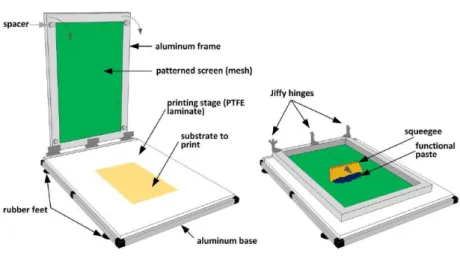
2.3.1 Screen printing
As illustrated in Figure2.2, screen-printing is based on a squeegee which provides shear stress to a paste making it flow through a patterned screen mesh, depositing a pattern onto versatile substrates with tailored surfaces and compositions from rigid to flexible substrates as well as materials either with smooth or rough surface.The paste flows through the open areas of the mesh thanks to the lowered viscosity of the paste provided by the squeegee. The system used in this work is manual and therefore many variables are taken in account such as printing speed, angle and geometry of the squeegee, mesh size, material, strength and snap-off(distance between screen and substrate), many
of which vary from user to user and affect replicability. This system can however be
automized, making the process faster and replicable. [5,25]
Applying printing techniques to the deposition of functional materials requires the formulation of suitable inks. Parameters such as viscosity, surface tension, wettability and adhesion to substrate need to be adjusted in order to provide optimal printing per-formance.
Viscosities, typically between 500-5000 cPs are referred to as desirable for screen-printing, since inks with low viscosity will run through the mesh rather than dispensing out of it. [5] One way of achieving these viscosities is by adding polymer binders, such as cellulose, which avoid excessive spreading and leakage through the mesh, providing a stabilizing and film-forming matrix hosting the semiconductive material that can adhere to a paper substrate. [6] Cellulose therefore plays a big role in printed electronics and will be covered in the following chapter.
To the best of the authors knowledge, the topic of printed inorganic semiconductors has been poorly explored, and more specifically, little is known when it comes to func-tionality of paper devices at room temperature. Pioneering work has been carried out by Carvalho et al. [5], where ZnO NPs electrolyte-gated transistors were developed taking advantage of screen-printing. However, the work resorted to high burn-out tempera-tures as well as the use of harsh chemicals such as toluene. An eco-friendlier approach has therefore been suggested, taking advantage of screen-printing with the final goal of producing EGTs at room temperature.
C H A P T E R 2 . I N T R O D U C T I O N
swellability, antimicrobial activity, biodegradable, enhanced mechanical properties. This has already led to applications such as antimicrobials, functional chemical sensing and biosensors. [27]
A custom-made screen printing station, illustrated in the following Figure2.2, was used to develop the EGT transistors, present at CENIMAT|i3N.
Figure 2.2: Schematic drawing of custom-made screen-printing system used at CENI-MAT|i3N. [25]
2.4 Cellulose
Cellulose is nature’s most abundant biopolymer resource. The main source of cellulose can be found in plant cell walls, but also some sea organisms, fungi and bacteria. It’s bio-compatibility, high elastic modulus, thermal stability, nontoxicity and low density makes it suitable for a wide range of applications, from paper and textile, food, pharmaceutical and chemical industry to disposable electronics. [1]
However, processing cellulose is still a challenge due to its rigid long-chain and strong intermolecular and intramolecular hydrogen-bonded structure, making its dissolution without chemical modification or derivitization difficult. Cellulose is therefore converted
into derivatives which are easily dissolved in ordinary solvents. Some examples are ethyl cellulose (EC), hydroxypropyl cellulose (HPC), methyl cellulose (MC), sodium car-boxymethyl cellulose (CMC) and cellulose acetate (CA). [1,8]
By combining cellulose or its derivatives with conductive materials through doping, blending or coating, new functional composite materials can take place in the form of microspheres, fibers or membranes, with the electroconductive material dispersed on the surface or within the matrix. This approach is an extremely attractive, inexpensive and advantageous approach, allowing the combination of electrical properties with high hydration, swellability and biocompatibility properties inherent of cellulose compounds, with applications as thickening, water-binding, suspension, stabilizing and emulsifying agents [1,6]
2 . 4 . C E L LU LO S E
C
h
a
p
t
e
r
3
M a t e r i a l s a n d M e t h o d s
This chapter aims to describe all the steps that were taken to develop and character-ize EGTs on paper. The first step explains the formulation of the cellulose composite semiconductor inks based on ZnO NPs forming printable inks compatible with screen-printing. The following step consists of the characterization of the printed films. Lastly, the application and characterization of the flexible EGTs is described, covering the fol-lowing topics: concentration of functional material, concentration and type of cellulose derivatives, number of printing passes, paper substrate, annealing time and temperature.
3.1 Formulation of the cellulose semiconducting composite
inks
All reagents were used as received. Deionized water (Millipore) was used in all ex-periments. Carboxymethyl (CMC) and hydroxypropyl (HPC) cellulose were explored as cellulose derivatives, for which two cellulose solutions were prepared, and both were com-pared to ethyl cellulose (EC) using the ink developed by Carvalho et al. as the reference. [5]
The EC solution was prepared previously by dissolving 5 wt.% ethyl cellulose 300 cP (CAS: 9004-57-3, Aldrich) on an 80:20 toluene/ethanol solution (CAS: 108-88-3/ CAS: 64-17-5) and then adding 40 wt.% of ZnO nanopowder, < 100 nm particle size (CAS:
1314-13-2), to this solution. [5]
Aqueous solutions of CMC with different viscosities were prepared varying the amount
of CMC (average Mw≈250.000, CAS: 9004-32-4, Aldrich) from 3 to 5 wt.%. After
C H A P T E R 3 . M AT E R I A LS A N D M E T H O D S
prepared. The HPC cellulose solutions were prepared by varying the amount of hydrox-ypropyl cellulose (average Mw 100.000, CAS: 9004-64-2, Aldrich) from 5 to 15 wt.% in ethanol (CAS: 64-17-5). Dissolution also takes around 3 hours stirring at 300 rpm. Different concentrations of ZnO nanopowder (40 wt.% and 50 wt.%) were added to the
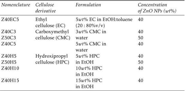
previously prepared HPC solution. Continuous stirring is necessary until complete dis-persion, for both derivatives. Table 3.1summarizes all of the developed inks and their constituents, with a nomenclature for each ink to simplify description.
Table 3.1: Table summarizing all developed inks with a nomenclature for each formula-tion.
Nomenclature Cellulose Formulation Concentration
derivative of ZnO NPs (wt%)
Z40EC5 Ethyl 5wt% EC in EtOH:toluene 40
cellulose (EC) (20 : 80%v/v)
Z40C3 Carboxymethyl 3wt% CMC in 40
Z50C3 cellulose (CMC) water 50
Z40C5 5wt% CMC in 40
water
Z40H5 Hydroxipropyl 5wt% HPC 40
Z50H5 cellulose (HPC) in EtOH 50
Z40H10 10wt% HPC 40
in EtOH
Z40H15 15wt% HPC 40
in EtOH
3.2 Characterization techniques
In order to find the best formulation composition and printing conditions, several characterization techniques were used to study the formulated inks as well as the result-ing printresult-ing patterns deposited on different paper-based substrates namely office paper,
FS2 paper and tracing paper.
Thermogravimetric and differential scanning calorimetry (TG-DSC) measurements
were also carried out on the semiconductor ink to study its thermal degradation using a Simultaneous Thermal Analyzer (TG-DSC – STA 449 F3 Jupiter), from room temperature to 550 °C with a heating rate of 5 °C/min, in an aluminium crucible, under ambient conditions.
Fourier Transform Infrared spectroscopy was used in order to study the drying con-ditions. The ZnO inks were screen-printed onto glass substrates, previously cleaned in acetone, IPA and DI water and then exposed to three different annealing temperatures, 25,
60 and 120 °C on a hotplate, for different times. The spectra was acquired at room
tem-perature between 4500 and 500cm−1 using a Thermo-Nicolet 6700 spectrophotometer
from Thermo Electron Corporation operating in attenuated total reflection (ATR) mode.
3 . 3 . FA B R I CAT I O N A N D C H A R AC T E R I Z AT I O N O F E L E C T R O LY T E - GAT E D T R A N S I S TO R S O N C E L LU LO S E - BA S E D PA P E R S U B S T R AT E S
The morphology of the printed semiconductor layers was analyzed by scanning elec-tron microscopy (SEM) using a Carl Zeiss AURIGA CrossBeam workstation instrument. Samples were coated with a thin layer of iridium ( 15 nm thickness) using a Q300T D Quorum sputtering system.
The structural analysis of the samples printed on glass substrates was obtained by X-Ray Diffraction (XRD) using a PANalytical X’Pert Pro-x-ray diffractometer.
3.3 Fabrication and characterization of electrolyte-gated
transistors on cellulose-based paper substrates
The conductive ink used for the patterning of source, drain and gate electrodes (il-lustrated in Figure2.1) consisted of a carbon paste (TU-10s, Asahi Chemical Research Laboratory Co., Ltd). The conventional pattern (W = 2000µm, L = 100µm, W/L = 20) was defined using a screen mold made of polyester with the following conditions: mesh model, 77-55; mesh count, 190 mesh/inch; aperture, 81 µm; thread diameter, 55µm;
opening, 30%; fabric thickness, 88-97µm. The carbon electrodes were cured at 70 °C for 30 min in air.
The semiconductor layer was printed with a different polyester screen mold with the
same characteristics of the one used to define the carbon electrodes and dried at room temperature. The gap between the gate electrode and the printed semiconductor layer is 400µm. Lastly, the CHE was cut, transferred and laminated onto the devices to connect
the transistors’ channel and gate electrode.
C
h
a
p
t
e
r
4
R e s u lt s a n d D i s c u s s i o n
4.1 Characterization and properties of cellulose composite
semiconducting inks and resulting printed patterns
This section will focus on the development of inorganic semiconductor inks compat-ible with screen-printing and paper electronics. The aim is therefore to use low-cost abundant materials naturally found on Earth and environmentally friendly, with the goal of developing eco-friendly inks.
The first step consist of developing several inks in order to find out the best combina-tion of components (cellulose derivative as binder vs. ZnO as funccombina-tional material) search-ing for semiconductsearch-ing properties of the resultsearch-ing cellulose composite printed layer on cellulose-based paper substrates at room temperature. In this work, the figures of merit which were taken into account for the formulation of the ZnO NPs ink were the type of cellulose derivative (HPC, CMC and EC) and its concentration, and the concentration of functional material.
4.1.1 Influence of binder and functional material concentration on print quality of the cellulose composite semiconducting inks
C H A P T E R 4 . R E S U LT S A N D D I S C U S S I O N
4.1.2 Influence of drying conditions on solvent evaporation from the printed cellulose composite semiconducting layer
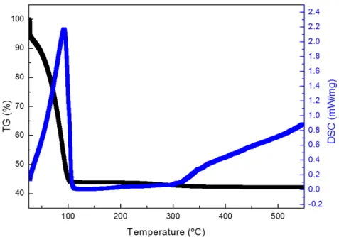
The thermal behaviour of the vehicle was studied via Thermogravimetric-Differential
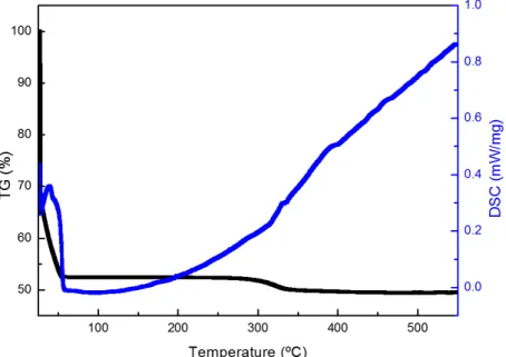
Scanning Calorimetry (TG-DSC). This way, the range of temperatures needed to burn out the vehicle can be established. The TG-DSC measurements were performed from room temperature to 550 °C. For Z40C3, the maximum peak of 2.15mW mg−1is observed for
92 °C as seen in Figure4.1, associated to an endothermic reaction. Considering that the solvent in this case is water which evaporates at 100 °C, a significant mass loss is observed at this temperature, which confirms the evaporation of the solvent. The ink is stable until around 250 °C, after which further mass loss suggests the beginning of CMC degradation. [5,6] It is noticeable that there is still ZnO powder present in the crucible until 550 °C since the data shows a positive mass value, reaching 40-50 % of initial mass for all ZnO NPs inks, the rest of which are shown in FigureII.1.
Figure 4.1: TG-DSC curves of Z40C3 ink.
For the HPC-based inks, maximum peaks of 0.35mW mg−1at 39 °C, 0.37mW mg−1
at 66 °C and 0.4mW mg−1at 66 °C are observed for Z40H5, Z40H10 and Z40H15 inks,
respectively, associated to an endothermic reaction, which in turn is associated to the evaporation of the solvent. Figure4.2shows the TG-DSC curves of Z40H5 ink. A compar-ison of all the TG-DSC curves are shown in AnnexII. The HPC-based inks are stable until around 300 °C after which further mass loss suggest the beginning of HPC degradation. For temperatures above 350 °C there is no notable mass loss suggesting that HPC was fully degraded. In conclusion, CMC and HPC-based inks are thermally stable under 250
4 . 1 . C H A R AC T E R I Z AT I O N A N D P R O P E R T I E S O F C E L LU LO S E COM P O S I T E S E M I CO N D U C T I N G I N K S A N D R E S U LT I N G P R I N T E D PAT T E R N S
and 300 °C, respectively. According to that and, since water and ethanol have boiling points below 100 °C (100 and 78 °C, respectively [1]) the influence of drying conditions on the print quality and electrical performance of the printed patterns was studied.
Figure 4.2: TG-DSC curves of Z40H5 ink.
This next part will focus on the annealing process but this time on ZnO NPs ink screen-printed on glass substrates. The idea is to verify through the Attenuated Total Reflectance-Fourier Transform Infrared Spectroscopy (ATR-FTIR), if thick films exhibit the same behaviour in relation to the increase in temperature, as in the previous subsec-tion concerning their ink form.
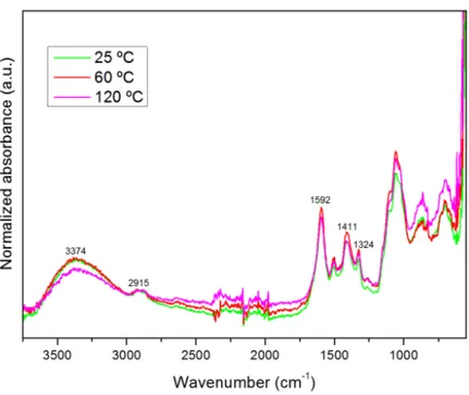
The drying conditions of the water content within the printed patterns of ink for Z40C3 was studied considering the obtained FTIR spectra. Figure 4.3shows the FTIR spectra for 25 °C, 60 °C and 120 °C. The spectra are normalized by the 2900cm−1band
which is quite insensitive to variations in the composition, crystallinity and water content of the cellulose. The spectra show that the carboxymethyl and hydroxyl functional groups the following peaks: the peak at 1592cm−1is related to C=O of -COO carboxyl group;
1411 cm−1 corresponds to -OH stretching; 1324 cm−1 is related to -C-H stretching in
symmetric planes of the CMC group. The broad absorption band at 3374 cm−1 is due
to stretching frequency of hydroxyl group (-OH) and can be associated with the water content within the printed patterns, which is the main band of interest to study water evaporation. The band at 2915cm−1 is due to carbon-hydrogen (C-H) stretching. [5,6, 28]
There is a notable reduction in the peak at 3374cm−1for 120 °C, indicating that with
C H A P T E R 4 . R E S U LT S A N D D I S C U S S I O N
Figure 4.3: FTIR spectra of Z40C3 for three temperatures, 25, 60 and 120 °C.
sample. Between 25 and 60 °C, the peak is coincident, meaning that between these two temperatures, drying at room temperature is more convenient. Even though at 120 °C the water content is the least, the objective for this work was to explore working conditions at room temperature which also simplifies the process, which is why the drying temperature was set at room temperature.
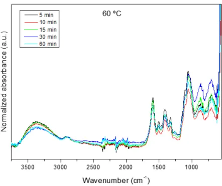
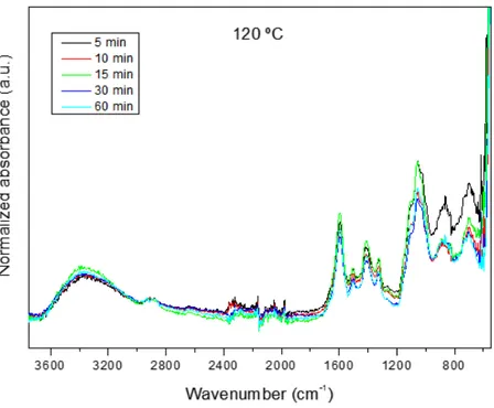
Figures4.4, 4.5and4.6 show the FTIR spectra for Z40C3 varying with time, at 25, 60 and 120 °C, respectively. For 25 °C, there is no significant reduction in the broad absorption band around 3374cm−1. However for 60 °C, there is a clear reduction in the
same peak over time, which corresponds to a greater reduction in the amount of water over time, whereas for 120 °C, these results are less apparent. These results show that annealing of these inks can be carried out at room temperature, on paper substrates, reducing the device fabrication process steps by avoiding high temperature and vacuum processes.
4 . 1 . C H A R AC T E R I Z AT I O N A N D P R O P E R T I E S O F C E L LU LO S E COM P O S I T E S E M I CO N D U C T I N G I N K S A N D R E S U LT I N G P R I N T E D PAT T E R N S
Figure 4.4: FTIR spectra of Z40C3 for 25 °C varying with time.
C H A P T E R 4 . R E S U LT S A N D D I S C U S S I O N
Figure 4.6: FTIR spectra of Z40C3 for 120 °C varying with time.
4.1.3 Structural and morphological characterization of the printed cellulose composite semiconducting layer
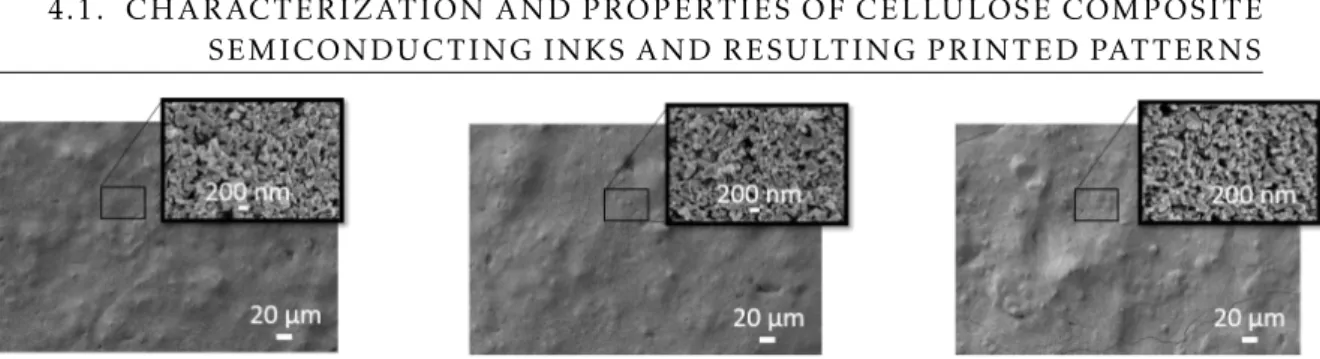
Morphology of the ZnO NPs in the ink printed onto different paper substrates was
examined by SEM. As can be seen in Figures4.7,4.8and4.9, all samples demonstrate agglomerates and macropores, which may be due to undispersed ZnO NPs in the solvent and rapid solvent evaporation, respectively. For the CMC-based samples, the morphology of the film remains the same except for FS2 paper, presenting some fissures. Comparing to the HPC-based based inks, the CMC-based samples present a smoother and homoge-neous surface. Cellulose fibers are most visible in H5Z40 samples, and in all samples, nanospheres, hexagonal nanorods and tripods are visible. Cracks in the semiconductor film can be seen more visibly for the HPC based inks (Figure4.8and Figure4.9), which may be due to rapid drying of the solvent (ethanol). A fast evaporation of the solvent leads to a poorly organized layer, increasing surface roughness. [29] Regarding the HPC-based samples, a higher concentration of HPC provides a smoother surface and less visible agglomerates.
The type of paper substrate which presents better uniformity and replicability is the office paper.
Figures4.7,4.8,4.9show a comparison of all the printed inks, side by side.
4 . 1 . C H A R AC T E R I Z AT I O N A N D P R O P E R T I E S O F C E L LU LO S E COM P O S I T E S E M I CO N D U C T I N G I N K S A N D R E S U LT I N G P R I N T E D PAT T E R N S
Figure 4.7: SEM images of Z40C3 ink printed on different substrates, from left to right,
office paper, tracing paper and FS2 paper.
Figure 4.8: SEM images of Z40H5 ink printed on different substrates, from left to right,
office paper, tracing paper and FS2 paper.
Figure 4.9: SEM images of Z40H15 ink printed on different substrates, from left to right,
office paper, tracing paper and FS2 paper.
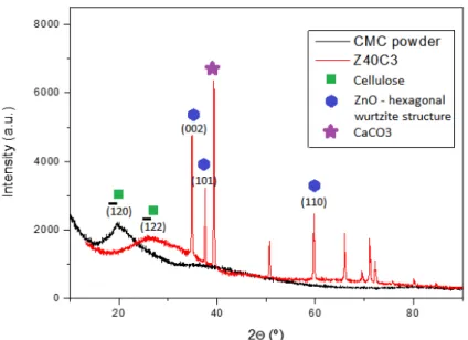
XRD diffractograms for the developed inks are shown in Figure4.10and Figure4.11.
In Figure4.10, there is a broad peak at 2Θ= 19.60°, (120), and in Figure4.11, the XRD diffractogram shows a broad peak at 2Θ= 19.94° (110), characteristic of CMC and HPC respectively (ICDD File: 00-056-1717). [5,30,31] However, for Z40C3 and Z40H5, the broad cellulose peak seems to dislocate to 2Θ = 26.36° (122) and 2Θ = 24.38° (200), respectively. Various factors could influence this apparent change in planes. The fact that glass substrates were used might influence the change in 2Θand therefore the planes, as well as possible interference of ZnO. The broad peak could also simply be associated to glass, due to the used glass substrates, and not to the suggested cellulose planes.
As to Z40C3, the distinct diffraction peaks at 34.88, 37.52 and 59.71° correspond to
(002), (101), and (110) planes, respectively, evidencing the formation of zinc oxide with a hexagonal wurtzite structure, in accordance with literature. [5,20] On the other hand at 39.36° calcium carbonate (CaCO3) is observable, which is due to the use of pigments
C H A P T E R 4 . R E S U LT S A N D D I S C U S S I O N
For Z40H5, distinct diffraction peaks at 31.70, 34.34, 36.18, 56.54° correspond to the
(100), (002), (101), and (110) planes, respectively, of a hexagonal wurtzite structure with hexagonal symmetry. [5] At 47.48°, the presence of CaCO3is also observed.
The crystallite size of both samples was calculated by the Debye-Scherrer method. This comes to approximately 17 nm for both samples and is in accordance with the particle size observed by SEM.
Figure 4.10: XRD diffractogram of CMC powder and Z40C3.
Figure 4.11: XRD diffractogram of HPC powder and Z40H5.
4 . 2 . E L E C T R I CA L C H A R AC T E R I Z AT I O N O F P R I N T E D Z N O T R A N S I S TO R S O N PA P E R
4.2 Electrical characterization of printed ZnO transistors on
paper
4.2.1 Influence of ink formulation
In this subsection, the influence of the ink formulation on the performance of the devices will be studied. This takes in account the type of cellulose derivative used in the ink formulation, its concentration as well as the ZnO NPs concentration for each ink. For these devices, all of the layers apart from the dielectric have been deposited by screen-printing. The theoretical value for the width (W) and length (L) of the electrodes are 2000µme 200µm, respectively. However, the determined value for W and L are 2072
±51µmand 136±30µmon average, respectively. This deviation in values is related to
screen-printing variations, more specifically, the spreading of ink which leads to wider W and shorter L values. In AnnexIan image of the screen-printed carbon contacts is displayed as well as a table with the considered number of samples for the determination of an average of W and L.
Table 4.1 provides the resume of the main electrical parameters obtained for the EGTs, which include turn-on voltage (VOn),IOn/Of f, transconductance (gm, (∂IDS/∂VGS)), subthreshold swing (SS) and saturation mobility (µsat). The electrical parameters were
obtained in the forward sweep direction, from negative to positive gate voltage, with
VDS=1 V and a scan rate of 200 mVs−1. The SS was calculated according to Equation4.1:
SS= ∂logIDS
∂VGS max
!−1
(4.1)
The saturation mobility (µsat) of the devices was determined through Equation4.2:
µsat = ∂
√
IDS
∂VGS
!2 2
L
W C (4.2)
WhereIDSis the drain current,VGS is the gate voltage, C is the capacitanceCDLof the
CHE, and W and L correspond to the width and length of the channel, respectively. The specific capacitance C of the ion gel is required for calculation of field-effect mobilities.
This has been determined by Cunha et al.[8] to be 5µF cm−2for the CHE in use.
Office paper was chosen as the substrate, since, in accordance to the previous chapter,
it presented best uniformity and replicability of the printed films. Figure4.12shows the transfer curves of the developed inks on office paper, underlying the influence of polymer
and ZnO NPs concentration, followed by table4.1summarizing the electrical character-ization. The developed inks have been summarized in a specific notation according to Table4.1, and the number of samples tested for each formulation was 5.
The devices exhibit a typical n-type behavior and low operating voltage (<2.5 V). The Ion/of f ratio for the CMC-based EGTs ranges from three to almost five orders of
C H A P T E R 4 . R E S U LT S A N D D I S C U S S I O N
Figure 4.12: Influence of the formulation of the semiconducting inks, dried at room tem-perature, on the transfer curves: polymer concentration (top) and ZnO NPs concentration (bottom).
Table 4.1: Electrical parameters of the EGTs considering CMC and HPC
Substrate VOn(V) IOn/Of f gm (mS) SS (V/dec) µsat(cm2V−1s−1)
Z40C3 0.7±0.21 (8.26±2.84)×104 0.41±0.13 0.25±0.09 8.9±2.8
Z50C3 0.3±0.29 (6.12±1.22)×103 0.2±0.17 0.29±0.13 2.9±3.8
Z40C5 0.5±0.43 (5.31±1.99)×103 0.2±0.15 0.2±0.1 0.3±1.9
Z40H5 1.2±0.22 (2.45±1.76)×104 0.2±0.06 0.1±0.1 4.1±1.5
Z50H5 0.6±0.21 (3.47±1.35)×104 0.6±0.33 0.2±0.05 1.3±5.9
Z40H15 0.7±0.0 (3.58±1.54)×103 0.7±0.0 0.4±0.02 1.6±0.01
i.e., the output current change per unit input voltage change (∂IDS/∂VGS) is dependent
on the gate capacitance besides the aspect ratio. A highgm is desired for circuit design, as it allows the desired drain-source current to be achieved at lower operating voltages. [9,14]
The EGTs exhibit gate leakage currents of 10−6 A. The use of papers with thinner
fibers, making the paper surface smoother, could result in reduced leakage current. [14] Relatively to the subthreshold swing (SS), which corresponds to the necessaryVGS to alter
theIDS by one decade, the devices all show a SS lower than 1, which indicates that the
4 . 2 . E L E C T R I CA L C H A R AC T E R I Z AT I O N O F P R I N T E D Z N O T R A N S I S TO R S O N PA P E R
devices can modulate more current with a lowerVGS, lowering power consumption. [5,
8] The CMC-based EGTs vary between 0.2 and 0.29 V/dec and HPC-based EGTs vary between 0.1 and 0.4 V/dec. The highest SS is 0.4 Vdec−1, for Z40H15, and the lowest SS
(0.1 V/dec) for Z40H5.
It is important to note theµsat values of Z50C3 and Z50C5: the standard deviation
is higher than the average value, which is due to the high viscosity of these inks, which can affect the printing quality, i.e., formation of clusters, rough film surface and
non-homogeneous surface combined with the irregular surface of paper.
For both cellulose derivatives, it is noticeable that higher polymer concentrations and higher ZnO NPs concentrations yield lower Ion/of f ratios. The highestµsat values were
close to 9cm2V−1s−1, corresponding to Z40C3.
There is noticeable hysteresis which increases with faster scan rates, associated to a slow response of the ions toVGS. This observed hysteresis behaviour can be attributed to a
combination of ion migration and charge trapping effects. [14,22] For slowerVGS scan
rates, the ions have enough time to diffuse into the semiconductor, promoting
electro-chemical doping. Hysteresis is a bistability in the operational transistor current. It is shown as a difference in IDS values observed during forward and backward sweeps of
the gate voltage (VGS). [22] Hysteresis in the current-voltage characteristics has
poten-tial characteristics in nonvolatile memory devices, however it is unwanted in standard integrated circuits. [8]
The biggest difficulty encountered during the development of the EGTs was related
to the screen-printing of the devices. Short-circuits between S and D contacts were frequently obtained which happened because of the ink spreading whilst being screen-printed, mostly due to nonuniform application of force and speed of the carbon ink layer. The semiconductor layer also proved difficult to reproduce since the alignment of the
mask in accordance with the previously deposited contacts depended not only on ink spreading, velocity and applied force, but also on the precision of the eye. These results therefore suggest that the best formulations consider the lowest polymer and ZnO NPs concentrations out of the formulated concentrations. Automatic screen-printing could also be used in order to avoid the previously mentioned screen-printing difficulties.
4.2.2 Influence of number of printed layers on EGTs performance
The influence of the number of printing passes of the semiconductor layer will be studied in this subsection. Up to five layers were screen-printed, with a drying period of around 5 minutes for each layer. Figure4.13compares the devices with different numbers
of semiconductor layers relative to the device performance, for Z40C3.
The results demonstrate a slight decrease of the electrical performance with the in-crease of semiconductor layers. The fact that the On current inin-creases (reducing the
C H A P T E R 4 . R E S U LT S A N D D I S C U S S I O N
Figure 4.13: Transfer curves of Z40C3 printed on office paper, comparing up to 5
semi-conductor layers.
Table 4.2: Electrical parameters of ZnO NPs ink printed on office paper, comparing up to
5 semiconductor layers.
Passes VOn(V) IOn/Of f gm (mS) SS (V/dec) µsat(cm2V−1s−1)
1x 0.8 8.26×10⁴ 0.41 0.25 8.9
2x 0.7 3.28×10⁴ 0.43 0.31 10.28
3x 0.6 2.04×10⁴ 0.25 0.35 5.02
4x 0.4 5.63×10³ 0.16 0.41 3.58
5x 0.5 2.07×10⁴ 0.39 0.41 7.87
increase of SS values. Therefore, surface roughness of the semiconductor layer must be reduced to provide maximum contact between semiconductor and electrolyte, resulting in better electrical performance.
There is a decrease in theVON with the increase of semiconductor layers. The results for 4 passes are not in accordance with the rest of the results and are therefore considered as an error in the screen-printing technique. These results continue to be dependent on the screen-printing technique and the small variations could be uncorrelated to the present study. The devices for the rest of this work were fabricated considering one layer of semiconductor ink to simplify the process.
The fact that only one layer of film is necessary in order to have a functional ZnO film at room temperature compatible with paper and without the need for sintering is very appealing in terms of simplicity for the fabrication of the devices.
4 . 2 . E L E C T R I CA L C H A R AC T E R I Z AT I O N O F P R I N T E D Z N O T R A N S I S TO R S O N PA P E R
4.2.3 Influence of drying conditions on EGTs performance
This next subsection will focus on the influence of the ink drying temperature on the electrical characterization of the devices. As done for FTIR-ATR, several devices were screen-printed on office paper and annealed at 25, 60 and 120 °C for 15 minutes. The
results are displayed in Table4.3. Z40C3 ink was used since it is the most reproducible ink with best results and 3 samples were used for each temperature. Figure4.14shows an example of the aspect of the printed Z40C3 film on office paper.
Figure 4.14: Aspect of printed semiconductor film for Z40C3, on office paper.
Figure 4.15: Transfer curves of printed ZnO EGTs on office paper and annealed at 25, 60
and 120 °C, showing three samples for each temperature.
Table 4.3: Electrical parameters of printed ZnO EGTs on office paper and annealed at 25,
60 and 120 °C.
Z40C3 VOn(V) IOn/Of f gm (mS) SS (V/dec) µsat(cm2V−1s−1)
25 °C 0.7±0.26 (8.26±3.50)×104 0.41±0.03 0.25±0.12 8.9±1.4
60 °C 0.7±0.15 (2.14±1.09)×103 0.40±0.20 0.28±0.05 9.7±4.5
120 °C 1.0±0.06 (4.05±8.64)×103 0.10±0.18 0.3±0.04 2.2±4.1
It is clear that annealing at 120 °C provides the worst results in terms ofµsat. This
C H A P T E R 4 . R E S U LT S A N D D I S C U S S I O N
the parameter values is elevated for the samples annealed at 60 and 120 °C, providing unreliable results. Thus, drying at room temperature is advantageous for the device performance and desirable for the fabrication of simpler, low cost and environmentally friendly devices.
4.2.4 Influence of cellulose-based paper substrate on EGTs performance
Taking advantage of the low processing temperature of the EGTs, other types of paper substrates were studied to compare electrical performance. Office paper, FS2 paper
and tracing paper were used as substrates for the devices (Figure 4.16). The electrical characterization is shown in Table4.4.
Figure 4.16: Transfer curves of printed ZnO EGTs on office paper, FS2 paper and tracing
paper using Z40C3 ink.
Table 4.4: Electrical parameters of printed ZnO EGTs using Z40C3 on office paper, FS2
paper and tracing paper.
Substrate VOn(V) IOn/Of f gm (mS) SS (V/dec) µsat(cm2V−1s−1)
Office 0.8±0.1 (8.26±3.50)×104 0.41±0.09 0.25±0.05 8.9±2.7
FS2 0.6±0.1 (8.20±4.69)×105 0.62±0.21 0.12±0.11 5.5±1.5
Tracing 0.5±0.4 (3.75±7.63)×103 0.13±0.07 0.35±0.02 2.2±1.6
FS2 paper had the highestIon/of f ratio (nearly 6 orders of magnitude) while office and
tracing paper allowed for anIon/of f ratio of 4 and 3 orders of magnitude, respectively. FS2
paper exhibits a much smoother and nanoporous surface contrasting with conventional printing paper. [1] This reduces surface roughness and therefore increases the device performance. [5] According to the output characteristics, the EGTs can reach highIDS
values at very lowVGS (2.5 V) andVDS (1 V) which are significantly higher for the office
paper EGTs. Tracing paper presents high standard deviation values for theIon/of f ratio, surpassing the average value, which is in accordance with the unreliability of the printed
4 . 2 . E L E C T R I CA L C H A R AC T E R I Z AT I O N O F P R I N T E D Z N O T R A N S I S TO R S O N PA P E R
film. The most reliable results originated from the office paper EGTs, which out of the
three papers, is the best choice.
4.2.5 Comparison of cellulose derivatives on EGTs performance
This subsection will focus on comparing the best formulations previously established from both cellulose derivatives, with an ethyl cellulose based formulation previously studied. [5] This will consider Z40C3, Z40H5 and Z40EC5, all with 40 wt.% ZnO NPs. The following Figure4.17compares these three formulations according to their electrical performance, followed by Table4.5summarizing these results.
Figure 4.17: Comparison of transfer curves from the three best formulations considering three cellulose derivatives.
Table 4.5: Electrical parameters of the printed ZnO EGTs on office paper considering
three samples for each of the three formulations.
Office paper VOn(V) IOn/Of f gm (mS) SS (V/dec) µsat(cm2V−1s−1)
Z40C3 0.7±0.26 (8.26±3.50)×104 0.41±0.03 0.25±0.12 8.90±1.37
Z40EC5 0.9±0.19 (2.59±0.89)×103 0.05±0.02 0.22±0.10 0.75±0.27
Z40H5 1.2±0.22 (2.45±0.18)×104 0.16±0.06 0.10±0.09 4.10±1.52
Figure4.18compares the gate leakage currents of each formulation, side by side. It is clear that the lowest leakage current originates from Z40C3, followed by Z40H5 and then Z40EC5.
All results still show some amount of hysteresis which can be reduced by decreasing paper roughness, compacting the paper, scaling down the built devices as well as reducing the gate electrode area. [5]
C H A P T E R 4 . R E S U LT S A N D D I S C U S S I O N
Figure 4.18: Comparison of transfer curves from the three best formulations considering three cellulose derivatives, showing each leakage current.
which is why the choice of the best ink will depend on the requirements and application. However, the high saturation mobility of Z40C3 (8.9cm2V−1s−1) as well as the easy
repro-ducibility of the semiconductor film makes this ink the preferable choice. Following these results, it is shown that the performance of both Z40C3 and Z40H5 surpass the perfor-mance of Z40EC5, not only in electrical characterization, but also by using eco-friendly solvents without the need for sintering, demonstrating the industrial applicability of these devices and an attractive alternative to previously formulated inks. [5]
C
h
a
p
t
e
r
5
C o n c l u s i o n a n d f u t u r e p e r s p e c t i v e s
5.1 Final conclusions
In this work, the main objectives were successfully achieved as follows:
1) The influence of different cellulose derivatives in regards to the semiconductors’ ink
performance in printed transistors were studied, with special attention on the dispersion of ZnO NPs in hydroxypropyl and carboxymethyl cellulose.
2) The developed cellulose-based inks were applied in flexible electrolyte-gated tran-sistors on paper at room temperature, taking advantage of screen-printing and using an ion gel based on a cellulose matrix with incorporated lithium ions. The electrical characterization of the ZnO NPs EGTs was performed in order to understand their per-formances.
Out of all the inks (in reference to Table 3.1), Z40C3 and Z40H5 presented best printing quality and reproducibility.
The study on drying conditions on solvent evaporation proved that CMC and HPC-based inks are thermally stable under 250 and 300 °C, respectively. Considering that the objective was to apply the cellulose-based inks at room temperature, the results prove it possible to implement these inks on flexible substrates such as paper.
Out of office paper, FS2 paper and tracing paper, office paper presented best
unifor-mity and replicability of the printed film.
Relatively to the best ink formulations, all devices exhibited a typical n-type behavior, low operating voltage (<2.5 V) and an Ion/of f ratio ranging from three to almost five
orders of magnitude. CMC and HPC-based inks both proved that higher polymer con-centrations and higher ZnO NPs concon-centrations yield lowerIon/of f ratios. The bestIon/of f
ratio encountered resulted from Z40C3 with a ratio of 8.26×10⁴, along with the highest
C H A P T E R 5 . CO N C LU S I O N A N D F U T U R E P E R S P E C T I V E S
the most reproducible ink.
Between the three types of tested paper substrates, FS2 paper had the highestIon/of f
ratio (nearly 6 orders of magnitude) whilst office and tracing paper allowed for anIon/of f
ratio of 4 and 3 orders of magnitude, respectively. Despite this, EGTs with office paper as
substrate proved the most replicable and therefore reliable choice.
The final comparison of cellulose derivatives showed that Z40C3 and Z40H5 both outperform Z40EC5 in electrical performance, with Z40C3 being the outstanding ink.
5.2 Future perspectives
Previous work by Carvalho et al. [5] showed that by using only screen-printing, ZnO NPs EGTs could be developed. This work showed great improvements by developing ZnO NPs EGTs, at room temperature, exploring different cellulose derivatives and using an
ion gel based on a cellulose matrix with incorporated lithium ions, thus improving device performance and simplifying the process as well as creating an eco-friendlier version of cellulose-based inks.
The use of an automatic screen-printing station would be beneficial, since many issues such as replicability and short-circuits between S and D contacts frequently obtained due to ink spreading because of nonuniform application of force and speed could be avoided. Consequently, a better understanding of the influence of snap-off, shear rate,
angle, geometry and squeegee type could be investigated.
For future work, it would also be interesting to focus on how the different polymers
af-fect the charge transfer between nanoparticles, including a study of channel conductivity in function of temperature.
This work brings new insights to advanced functional materials based on cellulose, toward a new generation of bioinspired electronics devices based on cellulose and inor-ganic functional materials. Cellulose has been explored extensively at CENIMAT/i3N and together with this work, this is certainly the beginning of challenging innovations as far as low-cost, flexible, eco-friendly electronics on paper is concerned.