Switching Arithmetic for DC to DC
Converters Using Delta Sigma Modulator
Based Control Circuit
K.Diwakar #1, V.Vinoth Kumar $2, N.Vignesh Prasanna#3 and D.Reethika*4 #
Department of Electronics and Communication Engineering
$
Department of Electronics and Instrumentation Engineering
*
Department of Computer Science and Engineering
#
Vel Tech University,Chennai, India.
*
St. Joseph’s College of Engineering, Chennai, India.
1
2
3
Abstract—In the proposed arithmetic unit for dc to dc converters using delta sigma modulator, a new technique is proposed for addition and multiplication of sampled analog signals. The output is in digital form to drive the converters. The conventional method has input signal limitation whereas in the proposed method the inputs can vary to full-scale. The addition of two discrete signals is done by sampling the two signals at a period called update period and feeding each signal to the input of signal dependant delta sigma modulator for half of the update period and combining the outputs for the update period. The extension of three discrete data addition can be carried out by using the same technique. For the multiplication of two discrete signals different method is adopted. One analog signal is fed to the input of first delta-sigma modulator (DSM1) after sampling. The sampled output of the second analog signal is negated or not negated depending on the bit state at the output of DSM1 and is fed to the input of second DSM(DSM2). The resulting bit stream at the output of DSM2 is the digital representation of the product of the sampled data of the two analog signals. In order to multiply three discrete data, the sampled output of third data is negated or not negated depending on the bit state at the output of DSM2 and is fed to the input of third DSM(DSM3). The resulting bit stream at the output of DSM3 is the digital representation of the product of the sampled data of the three analog signals. Using the proposed adder and multiplier circuits any expressions can be evaluated such that the average value of the digital output of the arithmetic unit over the update period gives the value of expressions during that period. The digital output of the arithmetic unit is used to drive the dc-dc converters.
Keywords— Adder, Arithmetic unit, DSM and Multiplier. I. INTRODUCTION
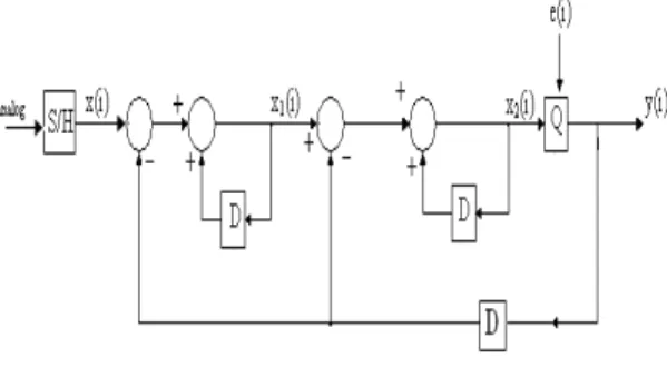
In the conventional discrete second order DSM [1],[2] sampling of input signal and DSM operation is performed by single clock signal with period TC and is shown in Fig.1. The block D is the delay unit of one
clock period (TC) and the block Q is binary quantizer. In Fig.1, x(i), x1(i), x2(i) and y(i) represent the ithsample of
input signal, first integrator output, second integrator output and quantizer output respectively. The quantization error signal during ithsampling period is denoted as e(i).
Fig. 1 - Conventional Second-Order DSM
The average value of the digital output during update period TU (TU >>TC) , is equal to the average value of
normalized input is defined as the input signal divided by feedback gain. The DSM becomes unstable when the modulus of the input signal is above 0.5n.
In [3], is presented the design of a mixed-signal 64-bit adder based on the continuous valued number system (CVNS). The 64-bit adder is generated by cascading four 16-bit radix-2 CVNS adders. Truncated summation of the CVNS digits reduced the number of required interconnections in the system, which in turn reduced the design complexity and hardware costs. The normal adders are not suitable for driving dc-dc converters.
The analog multiplier which is proposed in [4] is used for power and energy measurement and the power is measured with an accuracy of ±0.25%. In [5] is proposed cmos four quadrant analog multiplier which gives better bandwidth and less power dissipation but the accuracy is not improved. In [6] is proposed analog multiplier using operational amplifiers and the linearity error in the multiplier is 0.09%.
The objective of this proposal is that the output of the conventional bridge type dc-dc converter is to be controlled by different variables according to an expression. The variables can take sampled analog data and binary data. In conventional dc-dc converters, the control signal is applied to the input of conventional DSM. The digital output of conventional DSM is used as trigger pulses for the conventional bridge type switching converters. The output of the switching converters is applied to a dc load. For example, if dc motor is used as load, the speed can be controlled in both the directions. Let the dc motor is to be controlled by four variables
a,b,x and y. The variables can be analog or binary. The analog variables can be the demand signal from the operator, load cell signal, feedback signal etc. The binary signal can be the status of end limit switches, motor temperature switch, brake oil pressure switch etc. For example, consider the control expression (a+b)xy which involves the basic arithmetic operations like addition(subtraction) and multiplication(division).Let the DSM supply voltage is -10V and +10V and let each variable a,b,x and y can range from -10V to +10V.
The drawback of the conventional DSM is that when the magnitude of the normalized input exceeds 0.5, the conventional DSM becomes unstable [1],[2]. When the DSM is unstable the average value of the digital output is not equal to the average value of the discrete input over a period. If conventional DSM is used, the stable input signal range is -0.5n to +0.5n. Hence, the input signal is to be attenuated to -0.5n to +0.5nafter doing conventional analog addition and conventional analog multiplication. In the proposed DSM based arithmetic unit, the input signals are not attenuated and can range to full-scale and hence has better accuracy which depends on the arithmetic expression. The error signal is 0.025V in the proposed arithmetic unit when the expression (a+b)xy is evaluated. The percentage of error signal is 0.02% and the proposed arithmetic unit is better when compared to the multiplier which is proposed in [6]. The main advantage is that the output of the arithmetic unit gives the digital equivalent of the control expression and can drive the dc-dc converters directly through driver circuits for the full-scale range of the control variables.
II. PROPOSED ARCHITECTURE UNIT
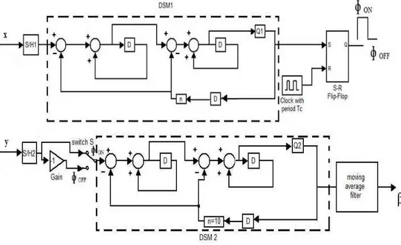
A. Block diagram of proposed signal dependent DSM
The block diagram of the proposed signal dependent DSM is shown in Fig.2. The main advantage of the proposed DSM is that it can function for the full scale range of the input signal. The S/H1 circuit samples the input signal i.e output signal from the proposed adder at a sampling period TU/2 and is denoted as z(i) or simply
z . The normalized input signal (znor = z/n) can range from -1 to +1 where n is feedback gain constant. The
sampled signal z is fed to the input of DSM. The sampled signal z is also used to control the operating period of DSM. The DSM circuit is operated by clock with period TC. The feedback gain is given by n|z|. The value of n
is selected to be greater than unity to satisfy the necessary condition for stability that the input z should be less than the feedback gain. Since the gain element is inserted in the feedback path, the average value of the output during each update period will be divided by the gain of the feedback path. In order to compensate the effect of signal dependant feedback gain, the operating time TO of the DSM circuit during each update period is varied
proportional to z. Therefore,
(1)
where k is the constant of proportionality. Substituting in (1) that when =n, results in . Substituting the value of k in (1), gives the value of TO as;
(2)
TU and TC are selected such that TU >> TC. The average values of outputs of the first integrator, second
integrator, and quantizer during ith update period are denoted as z1, z2and α respectively and the average value
of the quantizer error signal during ithupdate period is denoted as e. The sign block is used for a single bit
|
|
z
k
T
O=
|
|
|
|
z
=
z
maxquantizer. If the input signal to the sign block is above zero, the output is +1. If the input is less than zero, the output is -1and if the input is zero, the output will be zero. During a positive transition of update signal, the SR flip-flop is set. When the SR flip-flop is set (phase Φon), the switches s1 to s7 are closed (shown by thin dotted
lines) and DSM starts functioning. The DSM output consists of a sequence of pulses of magnitude +1,-1and 0. The resolution of DSM output, Δα is given by,
(3)
The resolution Δα is used to control the operating period of DSM such that the operating period is proportional to |z|. The resolution, Δα is integrated when the R-S flip-flop is set for a maximum period of TU/2.
The integral value of Δα, (Δα)cum is compared with |z|. When (Δα)cum>|z|, the SR flip-flop is reset (phase Фoff)
and the switches s1 to s7 are opened. DSM stops functioning and output is zero for the remaining sampling
period since the quantizer output is clamped to analog ground through the switch s8. All the integrators, denoted
as I1, I2, and I3 are reset to zero and cumulative addition of Δα also stops. Δα is selected such that (Δα)cum is less
than |zmax| (n). During next positive transition of update cycle the DSM operating cycle is repeated.
The time at which the states of different blocks are updated, is labeled on each block or on set of blocks (shown by thick dotted lines) in Fig.2. During each sampling period, the bit stream at the output of quantizer gives the digital representation of input signal. The output of the moving average filter (with gain
/ ) during
the period TU is equal to (a+b) in each update period. The timing–chart of the proposed DSM is shown in Fig.3.
For each period, TU/2(which is a constant), the DSM circuit operating time, TO (which is a variable proportional
to |z|) will be in the range 0 ≤TO ≤ TU/2.
In the proposed modulator znor can vary from -1 to +1 and the modulator is stable for the full range. The
input signal is over sampled at TU/2 and DSM input is dc signal for each sampling period because DSM is
operating at TC. For dc input if the DSM is operated with sufficiently low clock period the filter output during
TU(αi = α) will be a good approximation of the input.
Fig. 2 - Proposed signal dependent DSM
Fig. 3 - Timing Chart of Update Signal (Period TU), Clock Signal (Period TC ) and DSM Operating Signal (Duty TO in )
n
T
T
U C
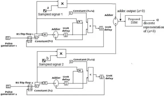
B. Block diagram of proposed adder
The proposed adder should add two analog signals a and b and should generate digital equivalent of a+b. Each variable can have maximum normalized value equal to unity. The proposed adder circuit is a combination of proposed multiplexer and proposed DSM. The block diagram of proposed adder circuit for switching arithmetic for dc-dc converters using delta-sigma modulator is shown in Fig.4. Both analog signals are sampled at TU. The ith samples are a(i) and b(i) but simply denoted as a and b respectively. The samples are combined
together such that the sample a is present for a period of 0 to TU/2 and the sample b is present for a period of
TU/2 to TU.
The pulse generator 1, generates a pulse of very short duration in the order of 0.1 µsec. and the period is
TU/2 without a phase delay. The pulse generator 2, generates a pulse of short duration with a period of TU/2 and
with the phase delay of TU/2.
The pulse generator 1, sets the flip-flop RS1. When RS1 is set, the value of clock period TC is continuously
added till the cumulative addition is equal to TU/2. Till this period, the sample of signal 1 is fed to the input of
analog adder. The other input of adder is zero and hence the output of conventional analog adder circuit is sampled signal 1 for a period of 0 to TU/2.
The pulse generator 2, sets the flip-flop RS2 after a delay of TU/2 and similar operation is repeated. The
result is that the output of adder is the sampled signal 2 for the next period of TU/2. The reason for doing such
addition of the two signals is that the normalized input signal range limitation of DSM should not be exceeded. The conventional method of adding two variables and generating digital equivalent for driving converters is by using conventional adder and conventional DSM. If conventional adder is used the maximum value of a+b
is equal to two. The maximum value of normalized input for which the conventional DSM is stable is equal to 0.5. Hence, conventional method of addition cannot be used for the full range of variables. In the proposed adder, multiplexing technique is used. The signal a is sampled at TU and fed to the proposed DSM for the first
half period of TU. The signal b is sampled at TU and applied to proposed DSM for the next half period of TU.
Hence, the maximum value of a+b never exceeds unity. The proposed DSM with signal dependant feedback gain operates for the full range of input signal. Since the normalized value of (a+b) falls within the range of -1 to +1, the signal dependant DSM can convert the full range of input signal to digital signal which will drive the converters. Ordinary analog addition of (a+b) before applying to the input of proposed DSM is not possible because the normalized value exceeds the full range of operation. Hence, this new technique for addition is proposed. Except the pulse generators and RS flip-flops, all the other blocks operate at the clock period TC. The
proposed DSM gives the digital representation of (a+b), when the proposed adder feeds at the input.
C. Block diagram of multiplier with two inputs
The block diagram of multiplier for two inputs (MUL2) is shown in Fig.5. In MUL2, only double sampling is used. The maximum normalized range of input signal for stable operation of DSM is limited by the condition that the integrators output should not exceed the maximum possible supply voltage. If the supply voltage of the circuit is 30V, the input signals can range from -0.98x30 V to +0.98x30 V. In Fig.5, the unit D represents a delay of one clock period. The first sample and hold circuit (S/H1) samples the input signal x at a sampling period TU. The sampled signal x is fed to input of DSM1. The DSM1 circuit is operating with clock of period TC
(TU >> TC). The SR flip-flop is reset (phase ФOFF) during each positive transition of clock signal. The output of
single bit quantizer, Q1 is in 1 state or in 0 state. When the quantizer output is in 1 state, SR flip-flop is set
(phase ΦON).
The second sample and hold circuit (S/H2) samples the input signal y at a sampling period TU. The DSM2
circuit is also operating with clock of period TC. The sampled analog input signal y is fed to input of DSM2
during phase ΦON. The variable y is negated and fed to DSM2 during phase ФOFF. During each sampling period,
the bit stream at the output of quantizer Q2, gives digital representation of product of sampled input signals. The
average value of bit stream at the output of Q2 during each sampling period namely β gives the discrete value of product of normalized samples of input signals ((x/n)×(y/n)) where n is feedback gain. Therefore, normalized value of β(βn) is equal to normalized product of input signals (xy/n).
Fig. 5 - proposed multiplier with two input (MUL 2)
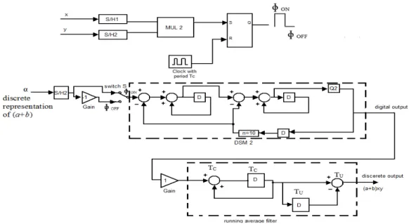
The multiplier with two-inputs can be extended for multiplication of multiple inputs. In Fig.6 is shown the method of extending two-input multiplier for multiplication of three inputs (MUL3). The output of MUL2 is in 1 state or in 0 state. When MUL2 output is in 1 state, SR flip-flop is set (phase ΦON). The third sample and hold
circuit (S/H3) samples the input signal α (proposed DSM output) at a sampling period TU. The DSM3 circuit is
also operating with clock of period TC. The input signal α is sampled and fed to the input of DSM3 during phase
Φon. The sampled signal is negated and fed to DSM3 during phase ФOFF .
During each sampling period, bit stream at the output of quantizer Q2 of MUL3, gives the digital
representation of product of sampled input signals. The output of the running average filter with gain
Tu Tcn k
2 .
= during each update period, gives the value of the arithmetic expression (a+b)xy. Ultimately, the
digital output from the quantizer Q2 of the proposed multiplier (MUL3) can be used as the trigger pulses for the
Fig. 6 - Proposed multiplier with three input signals (MUL3).
In Fig.7 is shown the conventional bridge type SC. The dc load is connected between the output terminals c
and d. When the discrete output of Fig.7 is +1, the switches Q1 and Q2’ are switched ON and the output terminal
c is +ve and d is –ve. When the discrete output is –1, the switches Q1’ and Q2 are switched ON and output
terminals d is +ve and c is –ve.
Fig. 7 - Conventional bridge type SC
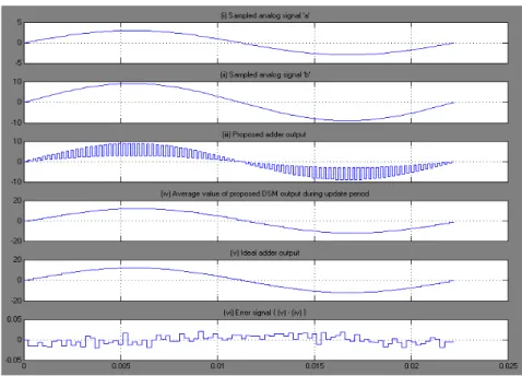
III. SIMULATIONRESULTS
The simulation is done using Matlab Simulink. In Fig.8, the first two waveforms show the input signals to the proposed adder. The output of the proposed adder is shown in Fig.8(iii).The output of the moving average filter with gain
2 /
2
Tu
Tcn of the proposed DSM which is used in the proposed adder is shown in Fig.8(iv).The
error signal which is obtained by comparing the outputs of the proposed adder and ideal adder is shown in Fig.8(vi).The maximum error signal is about 0.02V when the inputs varies from -10V to +10V.
Fig. 8 - Function of proposed adder (Horizontal axis- Time in sec., Vertical axis- Voltage in volts;TU =2.442 msec. and TC = 0.1μsec)
Fig. 9 - Functioning of proposed arithmetic unit. (Horizontal axis- Time in sec., Vertical axis- Voltage in volts; TU =2.442 msec., TC = 0.1μsec. and n = 10)
IV. CONCLUSION
The proposed switching arithmetic unit for dc-dc converter can evaluate all the arithmetic expressions such that the average value of the digital output of the arithmetic unit over the update period gives the value of expressions during that period. The variables can be analog signal or digital signal. The analog signal can take the full scale range. The maximum percentage of error while evaluating the expression (a+b)xy is 0.02% and is better than the recently proposed other multipliers
REFERENCES
[1] Norsworthy S. R., Schreier R. and Temes G. C. (1997) “Delta-Sigma Data Converters, Theory, Design and Simulation” New York, IEEE Press.
[2] Schreier R., Temes G.C.(2005) “Understanding Delta-Sigma Data Converters” IEEE Press.
[3] Mitra Mirhassani, Majid Ahmadi, and Graham A. Jullien, “Low-Power Mixed-Signal CVNS-Based 64-Bit Adder for Media Signal Processing” IEEE transactions on very large scale integration (vlsi) systems, Vol. 16, No. 9, September 2008.
[4] Giovanni Bucci, Edorado Fiorucci, Fabrizio Ciancetta,Daniele Gallo,Carmine Landi,Mario Luiso “Embedded Power and Energy Measurement System Based on an Analog Multiplier” IEEE Transactions on Instrumentation and measurement, Vol.62, No.8, August 2013.
[5] Nipa B. Modi, Priyesh P. Gandhi “Characterization of CMOS Four Quadrant Analog Multiplier” International Journal of Engineering Research and Applications (IJERA) Vol. 3, Issue 1, January -February 2013, pp.1276-1281.