Temperature and Deposition Time Efect on Properties and Kinetics of CdSe and
CdS
0.25Se
0.75Films Deposited by CBD
Elvia Angelica Sanchez-Ramireza,b, Maria de los Angeles Hernandez-Pereza*,
Jorge Ricardo Aguilar-Hernandezc, Elia Guadalupe Palacios-Beasa, Maricela Villanueva-Ibañezd
Received: June 06, 2016; Revised: May 04, 2017; Accepted: May 21, 2017
CdSe and CdS0.25Se0.75 thin ilms were grown by the Chemical Bath Deposition technique at diferent
temperatures (50-90°C) and deposition times (5-180 min). Both kinds of ilms are polycrystalline, constituted by nanostructured clusters of particles. CdSe ilms consist in a mixture of cubic and hexagonal phases (4-8 nm crystal size), whereas only the hexagonal phase is observed in the CdS0.25Se0.75 ones (6±1 nm crystal size). A decrease on the CdSe ilms density was observed due to the sulfur introduction into the crystal lattice. The composition of the ternary ilms is afected by both temperature and deposition time. The Band gap values (Eg) are afected by temperature, atomic composition and deposition time, decreasing from 2.09 to 1.93 eV, showing a quantum coninement efect mainly in the CdSe ilms. The ilms thickness, ranging from 30 to 600 nm, increases as a function of temperature and deposition time. Photoluminiscence signal is improved after thermal treatment, evidenced by the radiative broad bands observed at 1.84 and 2.20 eV.
Keywords: Nanostructured ilms, Semiconductors, Kinetics of deposition
* e-mail: [email protected]
1. Introduction
II-VI semiconductor compounds as thin ilms have been studied over the past decades. They can be prepared by several techniques such as laser ablation, spray pyrolysis, thermal evaporation, and chemical bath deposition (CBD), among others1-5. CBD ilms are obtained by spontaneous precipitation in alkaline medium, occurring when the ionic product exceeds the solubility product, by heterogeneous and homogeneous reactions taking place on the substrate and in the bulk solution respectively6; deposition occurs even at low temperatures and short times. This technique allows a close control on the ilm properties. CBD has been used to deposit several semiconductors including chalcogenide materials such as ZnSe, ZnS, CdS, CdTe and CdSe6-10. The need to develop new nanomaterials, expand their applications and improve their physical properties motivated the synthesis of complex ternary and quaternary compounds such as
CdSSe7,11-14, CdZnSSe7 and CoZnCdS15. Nanostructured CdSe thin ilms have been extensively studied and used in optoelectronic, photoelectrochemical and non-linear optics applications. The formation of ternary CdS1-xSex solid
solutions improves the physical properties of the binary CdSe. Tailoring the CdS1-xSex composition (x) allows the
enlargement of its response range in the visible spectrum, widening its applications. Notable achievements have been reported on the synthesis and characterization of CdS1-xSex
thin ilms by several techniques, most of them focused on the improvement of the optical, electrical and structural properties by modifying the composition. However, neither the kinetics of deposition nor the efect of temperature and time on the chemical nature of the ilms have been reported. In previous works, we reported the experimental procedure and the optimal Cd:S:Se bath atomic ratio to obtain CdS1-xSex
ilms with speciic compositions11,16. In the present study, the synthesis of CdSe and CdS0.25Se0.75 ilms carried out varying deposition time and temperature is reported, analyzing the efect of the variables and the introduction of sulfur ions into the CdSe crystal lattice on the structural, morphological and optical properties of the obtained ilms. Additionally, to understand the basic kinetics of the heterogeneous reaction, the growth rate, thickness and atomic composition were correlated with time and temperature. Low temperature photoluminescence measurements of CdS0.25Se0.75 were also performed to determine exciton recombination and/or free to bound transition.
aDepartamento de Ingeniería en Metalurgia y Materiales - ESIQIE, Instituto Politécnico Nacional,
Ciudad de México, 07738, Mexico
bDepartamento de Ingeniería Metalúrgica - UPIIZ, Instituto Politécnico Nacional, Zacatecas, 98160,
Mexico
cEscuela Superior de Física y Matemáticas, Instituto Politécnico Nacional, Ciudad de México, 07738,
Mexico
dLaboratorio de Nanotecnología y Bioelectromagnetismo Aplicado, Universidad Politécnica de
Sanchez-Ramirez et al.
1122 Materials Research
2. Experimental
2.1 Deposition
CdSe and CdS1-xSex ilms were deposited onto Corning
glass by the Chemical Bath Deposition (CBD) technique according to the procedure reported elsewhere1. 0.1M CdCl
2, 0.1M CS(NH2)2 and 0.1M Na2SeSO3 solutions prepared from analytical grade reagents were used as precursors. Deposition temperature was set at 50, 75 and 90°C. Alkaline pH of the bath was kept at 10.5 by adding 4M NH4OH; an excess of ammonia is required to avoid the formation of Cd(OH)2
17. 0.2M NH4Cl was used only for CdS0.25Se0.75 growth. To promote the homogeneity of the ilms, the precursors were pre-heated at the deposition temperature prior to be mixed. To obtain CdS0.25Se0.75 ilms it is necessary to employ an excess of Se16, therefore a 1:0.25:1.31 Cd:S:Se precursors ratio was employed. On the other hand, for the CdSe ilms the Cd:Se precursors ratio was kept at 1:1, as indicated in the literature1,11,18. The inluence of deposition time (5 to 360 min) on atomic composition, thickness and growth rate of the ilms was analyzed. Two atmospheres, vacuum (TT) and CdCl2 rich (TT CdCl2), were tested in order to improve the photoluminescence signal of the grown samples. Photoluminescence of CdS0.25Se0.75 ilms was measured from room temperature to 10K.
2.2 Films characterization
Structural properties were studied by X-ray difraction (XRD) employing a Bruker Advanced difractometer (Cu Kα=1.5406Å) operating in grazing angle (0.3-2°) coniguration. The surface morphology of the ilms was observed with a SEM JEOL JSM6701F equipped with an Energy Dispersive Spectroscopic (EDS) module. Optical absorption was measured using an UV-Vis spectrometer Perkin-Elmer Lambda35. Photoluminescence (PL) measurements were carried out by exciting with a He-Cd laser (442 nm), focused on the sample through a spherical lens; for the CdSe samples, a HeNe laser (633 nm, 1.9 eV) was also used. The outcoming radiation from the ilm was focused on a 1403-SPEX double monochromator and detected with a RCA-C31034 photomultiplier coupled to a photon counter, thermoelectrically cooled to improve the signal-noise ratio. The detected PL spectra were corrected for the spectral response of the system. A Sloan Dektak Proilemeter was used to measure the thickness of the samples.
3 Results and Discussion
3.1 Structural and morphological properties
As it is known, CdSe ilms crystalize in hexagonal2,3, cubic 4, 8, 18 or a mixture of both phases1,11. Films deposited
by using several techniques are polycrystalline in nature1-3. Figure 1a shows the XRD patterns of CdSe thin ilms grown at 50, 75 and 90 °C during 15 and 120 min. Due to the thin ilms obtained and the low crystalline quality of the samples, the substrate contribution for the ilms grown at 50 and 75 °C during 15 min is observed. As growth time and temperature increase, crystalline quality improves and four peaks become well deined, corresponding to the (100), (002), (110) and (112) planes of the hexagonal phase (JCPDS ile No 653436). Additionally, these relections, excepting that observed around 24.21°, match the (111), (220) and (311) planes of the cubic phase too (JCPDS ile No 882346). According to these results, ilms could have a mixture of both phases. Films show preferential orientation on (002) and (111) planes as previously reported in literature4,5,18. A small shift on the peaks position to higher angles from those corresponding to the JCPDS iles, observed in all ilms, can be associated to the presence of strains. In Figure 1b, two difraction peaks can be elucidated on the CdS0.25Se0.75 samples grown at 15 min, not observed in the corresponding CdSe XRD pattern. This result can be due to the higher thickness and better crystalline quality of the ilms, indicating a faster and more orderly crystallization rate in the case of the CdS0.25Se0.75 samples. As expected, the peaks are slightly shifted to higher angles (2θ=0.2°) due to the introduction of S into the crystal lattice of CdSe, resulting in the ternary solid solution formation. As reported in literature for CdS1-xSex12-13,19, CdS0.25Se0.75 ilms are
polycrystalline with hexagonal phase showing preferential orientation on the (002) plane related to the JCPDS iles No 50072. However, considering the similarity in the unit cell packing of cubic zinc blende and hexagonal wurtzite structures, the cubic phase contribution in these ilms could not be disregarded, as reported by Xie et al 12. In all cases, time and temperature increase both thickness and crystalline quality of the ilms, but there is no evidence of their inluence in the ilms strain. According to the crystal size values of the samples, estimated with the Scherrer’s equation using the full width at half maximum (FWHM) of the (111) and (002) planes, temperature does not afect the CdS0.25Se0.75 ilms (6±1 nm crystal size in all cases); regarding the CdSe ilms, the crystal size value slightly increases as temperature is increased, with estimated values of 4, 6 and 8 nm for the ilms grown at 50, 75 and 90 °C respectively.
Figure 1. XRD spectra of a) CdSe and b) CdS0.25Se0.75 ilms grown during 15 and 120 min at diferent temperatures.
Figure 2. High-resolution SEM micrographs of CdSe and CdS0.25Se0.75 ilms deposited during 15 and 120 min at diferent temperatures.
deposited during 15 min at 50 and 75°C show few clusters, that give rise by growth and coalesce to the denser ilms observed at 120 min. These results indicate that the XRD peaks deinition observed in Figure 1b is due to the higher crystalline quality of the CdS0.25Se0.75 ilms deposited at 15 minutes and not to their thickness, compared to CdSe. At the longest deposition time (120 min), the resulting ilms are denser, with similar morphology and narrower cluster size distribution than those obtained at shorter deposition times for all temperatures tested.
EDS analysis reveals an average 1.2:1 Cd:Se atomic composition for all the CdSe samples, suggesting that ilms possess Se vacancies at all time and temperature deposition
Sanchez-Ramirez et al.
1124 Materials Research
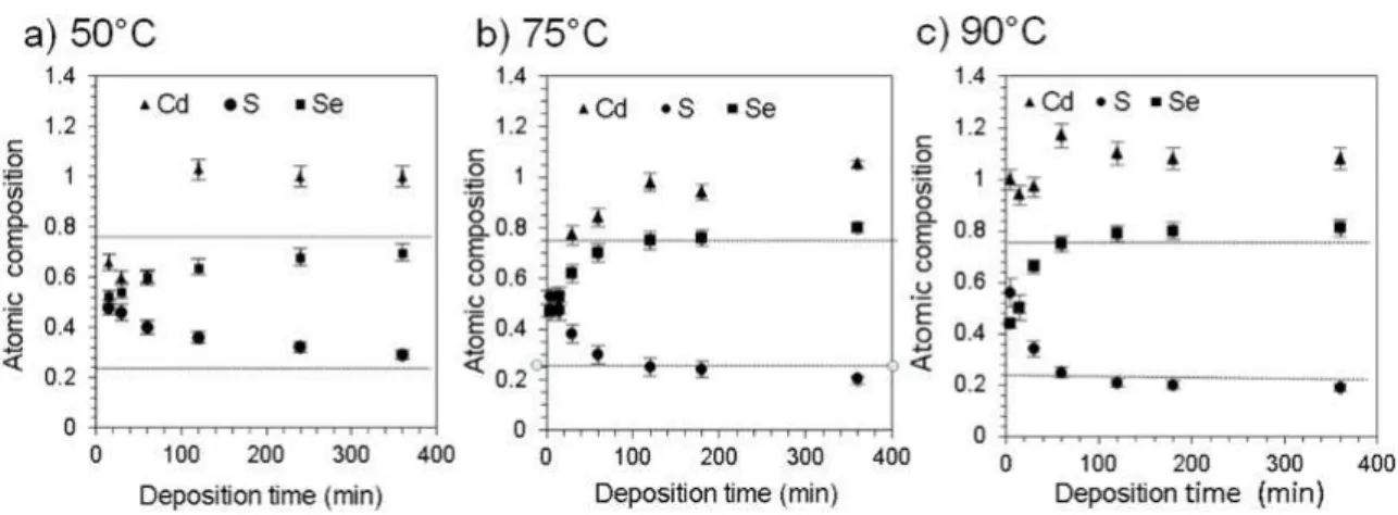
Figure 3. Efect of time on the atomic composition of CdS0.25Se0.75 ilms grown at a) 50, b) 75 and c) 90°C.
CdS0.25Se0.75, is obtained at 120 and 60 min for 75 and 90
°C respectively. For ilms prepared at 50°C, the expected composition is not attained even at 360 min, indicating that the sulfur substitution process is strongly accelerated by temperature. The Cd ion coeicient increases with both time and temperature, reaching a close to 1 constant value.
3.2 Optical properties
Optical properties of the CdSe and CdS0.25Se0.75 ilms were analyzed through absorption and photoluminescence studies. Figure 4a shows the absorption spectra of ilms deposited at 50, 75 and 90°C during 120 min, which were normalized with the highest signal in order to improve the comparison. A well-deined absorption edge is observed for all ilms, showing that ilms have good optical properties. Absorption edges of CdSe and CdS0.25Se0.75 ilms shift to red as a function of temperature. However, the addition of S to CdSe alloy provokes a blue shift of the absorption
Figure 4. a) Absorbance spectra and b) plot of (αhυ)2 vs (hυ) of CdSe and CdS
0.25Se0.75 ilms grown during 120 min at diferent temperatures.
edge. Considering that both CdSe and CdS0.25Se0.75 are direct band gap semiconductors, band gap values were estimated using the αhν=A(hν-Eg)1/2 equation, where α is
the absorption coeicient, A is a constant and n=1/2 for allowed direct transitions. The Eg value is obtained by extrapolation to α=0 in the (αh)2 vs h plot (Figure 4b) 11-12,20. As expected, E
g decreases according to temperature but increases with the formation of the ternary compound. The estimated CdSe Eg are 2.02, 1.96 and 1.90 eV for ilms grown at 50, 75 and 90°C respectively. These values are higher than Eg for the bulk material (1.74 eV) because of the small crystal size of the samples, as calculated from XRD (from 4 to 8 nm), whereby a quantum efect is predictable12,20-22. Regarding CdS
Figure 5. Energy band gap, Eg, of a) CdSe and b) CdS0.25Se0.75 ilms grown at diferent deposition time and temperature.
time on the Eg value for CdSe and CdS0.25Se0.75 ilms at diferent temperatures is depicted in Figure 5a and 5b respectively. In both cases, Eg decreases as a function of deposition time, until reaching a constant value for all temperatures. In the case of CdSe ilms, the decrease can be related to crystal size, which slightly diminishes too. However, as the crystal size for the ternary compound ilms is almost constant (6 nm), the reduction of Eg in this
case can be related to the change in the composition, as observed in Figure 3.
Figure 6a shows the room temperature photoluminescence results for the as-grown and the thermal-treated (TT) CdSe
and CdS0.25Se0.75 ilms. As it can be seen, no signal for the
as-grown CdSe samples was detected. Moreover, after the thermal annealing at 450°C, a broad band centered
Figure 6. a) Room temperature PL spectra of as grown and thermal treated (TT) CdSe and CdS0.25Se0.75 ilms and b) PL spectra of
CdS0.25Se0.75 ilms measured at diferent temperatures, 10≤T≤300K.
around 1.55 eV appears, it becoming better deined after annealing at 560°C. The PL signal at room temperature is signiicantly improved at annealing the CdS0.25Se0.75 sample with CdCl2 at 400°C; the spectrum shows two radiative broad bands, one at the low energy side, with a maximum around 1.84 eV and the second centered at 2.20 eV approximately. A similar spectrum has been already reported by Perna et al.23, corresponding to a CdS
0.2Se0.8, sample grown by laser ablation. Usually, those bands are related to deep levels, attributed to either sulfur or selenium vacancies, or else to non-radiative extrinsic defects due to structural disorders of the alloy. Figure 6b depicts the PL signal behavior with temperature corresponding to
the CdS0.25Se0.75 sample grown during 120 minutes. The
Sanchez-Ramirez et al.
1126 Materials Research
band observed at low temperature suggest that it is not due to exciton recombination. No noticeable shift of the bands can be observed. The high energy band could be assigned to transitions arising from native impurity levels, such as free to bound or donor-acceptor recombination.
3.3 Kinetics of deposition
The thickness of all the CdSe and CdS0.25Se0.75 ilms as a function of time and temperature are presented in Figure 7a and 7b, respectively. A typical time dependent S-shape curve is only observed in the CdSe ilms grown at 50°C as it occurs in just a few minutes17 it is rarely observed. In all other cases the thickness increase at a fast initial rate and the proiles show that the growth regime is taking place over six hours. It is clear that the introduction of S in the
Figure 7. Thickness of a) CdSe and b) CdS0.25Se0.75 ilms deposited at diferent time and temperature.
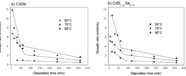
Figure 8. Growth rate variation of a) CdSe and b) CdS0.25Se0.75 ilms as a function of deposition time and temperature.
bath does not afect the thickness of the ilms, thus the kinetics of both CdSe and CdS0.25Se0.75 deposition is very similar. However, as already observed in Figure 2, ternary ilms deposited at short time (15 min) and low temperature (50°C) are less dense than binary ilms grown at the same conditions, thus nucleation of CdS0.25Se0.75 is slow and growth is extremely fast. The growth rate was estimated as the ratio between thickness (nm) and deposition time (min), Figure 8 presents the efect of time on growth rate of CdSe (a) and
CdS0.25Se0.75 (b) ilms. Growth rate strongly diminishes as
4. Conclusions
Nanostructured CdSe and CdS0.25Se0.75 thin ilms have been grown by CBD varying deposition time and bath temperature. CdSe ilms properties are modiied by the solid solution formation with the S ion added to chemical bath; better quality crystallization in hexagonal phase is promoted, Eg is increased but density of the ilms is diminished and no PL improvement is detected. Ternary ilms composition, x, depends on time and temperature while Cd:Se ratio of binary samples is not afected by these parameters. Temperature and time deposition promote high crystalline quality and the decrease of band gap values; concerning CdSe ilms this reduction is related to crystal size and in the case of
CdS0.25Se0.75 ilms it is associated to the composition change.
Room temperature PL of CdS0.25Se0.75 ilms is observed after annealing with CdCl2, two broad bands associated to cadmium or selenium vacancies and to structural disorder are observed. Low temperature PL of CdS0.25Se0.75 ilms indicates free to bound or donor-acceptor recombinations. The kinetics of the ilm formation is controlled by the chemical reactions taking place in both ternary and binary systems.
5. Acknowledgments
This work was supported by IPN-SIP contracts 20151801, 20161872 and 20161876. E.A.S.R. thanks the CONACYT and IPN for PhD and BEIFI grants.
6. References
1. Hernandez-Perez MA, Aguilar-Hernandez J, Contreras-Puente G, Vargas-García JR, Rangel-Salinas E. Comparative optical and structural studies of CdSe ilms grown by chemical bath
deposition and pulsed laser deposition. Physica E:
Low-dimensional Systems and Nanostructures. 2008;40(7):2535-2539.
2. Yadav AA, Barote MA, Masumdar EU. Studies on cadmium selenide (CdSe) thin ilms deposited by spray pyrolysis. Materials Chemistry and Physics. 2010;121(1-2):53-57.
3. Kumar V, Sharma DK, Sharma K, Dwivedi DK. Structural, optical and electrical characterization of vacuum-evaporated nanocrystalline CdSe thin ilms for photosensor applications.
Applied Physics A. 2016;122:960.
4. Hassanien AS, Akl AA. Efect of Se addition on optical and electrical
properties of chalcogenide CdSSe thin ilms. Superlattice and
Microstructures. 2016;89:153-169.
5. Chavan GT, Kamble SS, Chaure NB, Maldar NN, Deshmukh LP. Invoking stoichiometric protocols for chemical synthesis of CdSe thin ilms. Journal of Alloys and Compounds. 2016;680:139-145. 6. Pawar ST, Kamble SS, Pawar SM, Chavan GT, Prakshale VM, Chaure NB, et al. Constraints for ZnSe thin ilm growth and stoichiometry regulation. Journal of Materials Science: Materials in Electronics. 2016;27(10):10582-10591.
7. Deo SR, Singh AK, Deshmukh L, Susan MABH. Metal
Chalcogenide Nanocrystalline Solid Thin Films. Journal of
Electronic Materials. 2015;44(11):4098-4127.
8. Ben Nasr T, Kamoun N, Kanzari M, Bennaceur R. Efect of pH on the properties of ZnS thin ilms grown by chemical bath
deposition. Thin Solid Films. 2006;500(1-2):4-8.
9. Kim M, Sohn S, Lee S. Reaction kinetics study of CdTe thin ilms during CdCl2 heat treatment. Solar Energy Materials and
Solar Cells. 2011;95(8):2295-2301.
10. Šimurda M, Němec P, Formánek P, Němec I, Němcová Y, Malý P. Morphology of CdSe ilms prepared by chemical bath deposition:
The role of substrate. Thin Solid Films. 2006;511-512:71-75.
11. Sanchez-Ramirez EA, Hernandez-Perez MA, Aguilar-Hernandez JR, Contreras-Puente G. Bath atomic composition and deposition time inluence on the properties of nanostructured CdS0.5Se0.5
thin ilms synthesized by CBD. Materials Chemistry and
Physics. 2015;165:119-124.
12. Xie R, Su J, Liu Y, Guo L. Optical, structural and photoelectrochemical properties of CdS1xSexsemiconductor ilms produced by chemical
bath deposition. International Journal of Hydrogen Energy.
2014;39(7):3517-3527.
13. Siddiqui FY, Shaikh SU, Desale DJ, Upadhye DS, Mahajan SV, Ghule AV, et al. Band gap engineering by substitution of
S by Se in nanostructured CdS1−xSex thin ilms grown by soft
chemical route for photosensor application. Materials Science
in Semiconductor Processing. 2014;27:404-411.
14. Mariappan R, Ponnuswamy V, Ragavendar M. Characterization of CdS1−xSexthin ilms by chemical bath deposition technique. Optik - International Journal for Light and Electron Optics.
2012;123(13):1196-1200.
15. Kamble SS, Sikora A, Chavan GT, Pawar ST, Maldar NN,
Deshmukh LP. Design and fabrication of quaternary Co
1-x-yZnxCdyS thin ilms photoelectrochemical (PEC) cell. Materials Letters. 2017;186:247-251.
16. Sanchez-Ramirez EA, Hernandez-Perez MA, Aguilar-Hernandez J, Rangel-Salinas E. Nanocrystalline CdS1−xSexalloys as thin
ilms prepared by chemical bath deposition: Efect of x on
the structural and optical properties. Journal of Alloys and
Compounds. 2014;615(Suppl 1):S511-S514.
17. Hodes G. Chemical Solution Deposition of Semiconductor
Films. Boca Raton: CRC Press; 2002.
18. Khomane AS, Hankare PP. Structural, optical and electrical characterization of chemically deposited CdSe thin ilms.
Journal of Alloys and Compounds. 2010;489(2):605-608. 19. Kumar V, Dwivedi DK. Study on structural, optical and optical
properties of CdS0.5Se0.5 thin ilms for photovoltaic applications.
Optik - International Journal for Light and Electron Optics.
2013;124(16):2345-2348.
20. Hankare PP, Chate PA, Sathe DJ, Jadhav BV. X-ray and optical properties of chemically deposited nanocrystalline CdSe thin
ilms. Journal of Alloys and Compounds. 2010;503(1):220-223.
21. Ziabari AA, Ghodsi FE. Growth, characterization and studying of sol–gel derived CdS nanoscrystalline thin ilms incorporated
in polyethyleneglycol: Efects of post-heat treatment. Solar
Sanchez-Ramirez et al.
1128 Materials Research
22. Surendran S, Pokorný J, Jurek K, Bernstein E, Maly P. Temperature dependence of the optical energy gap of CdSSe
nanocrystals in glass. Materials Science and Engineering: B.
2003;104(1-2):54-57.
23. Perna G, Pagliara S, Capozzi V, Ambrico M, Ligonzo T.
Optical characterization of CdSxSe1−x ilms grown on quartz
substrate by pulsed laser ablation technique. Thin Solid Films.