Brazilian Journal of Physics, vol. 36, no. 2A, June, 2006 347
Energy Levels in Si and SrTiO
3
-Based Quantum Wells
with Charge Image Effects
T. A. S. Pereira, M. G. Bezerra, J. A. K. Freire, V. N. Freire, and G. A. Farias Departamento de F´ısica, Universidade Federal do Cear´a,
Campus do Pici, Caixa Postal 6030, 60455-900 Fortaleza-CE, Brazil
Received on 4 April, 2005
In the present work we develop a theoretical study to analyze how the image charges effects can modify the electronic properties inSiandSrTiO3-based quantum wells. We have used the method based on the calculation
of the image charge potential by solving Poisson equation in cylindrical coordinates. The numerical results show that the electron-heavy hole recombination energy can be shifted by more than 200 meV due to the combination of charge image andSiO2(SrTiO3)interface thickness effects.
Keywords: Energy Levels; Si;SrTiO3-based quantum wells
I. INTRODUCTION
The SiO2 gate thickness shrinkage to less than 50 ˚A is driving research efforts to find alternative oxides with high-k dielectric constant to allow for physically thichigh-ker films that can limit leakage current problems [1]. Recent research shows that SrTiO3, HfO2andTiO2 materials are the most promis-ing candidates to SiO2 replacement in development of new semiconductors devices. With the advances in the growth of SrTiO3 on silicon by epitaxy [2], the development of quan-tum confinement based optical devices is possible, following the steps of an original suggestion and demonstration of light emission inSi/SiO2 quantum wells (QWs) [3, 4], by simple replacement of silicon dioxide bySrTiO3. The understanding of the atomic structure at thesilicon/oxideinterface is still not complete. However, the ability to grow gate quality crystalline oxide films onSiin industrial scale is yet to be demonstrated. Droopadet al. [5] observed that the possible explanation for the formation of such an amorphous layer includes the diffu-sion of oxygen during the growth of the oxide layer reacting with the interfacialSiatoms. This would suggest that the in-terface layer is some form ofSiOxwithx≤2. Chamberset
al. [6] have shown that the interest in including an interfacial layer of SiO2suggests significant progress in order to reduce the leakage current, either because SiO2 acts as an electron tunnel barrier or because SiO2 at the interface increases the conduction band offset between SrTiO3andSi. Tuanet al. [7] show that theTiO2can not be grown directly onSibecause of thermodynamic instabilities, leading toTiSix andSiO2at the interface. However, TiO2 can be grown as an epitaxial film onSrTiO3(001) that can be grown epitaxially onSi(001) with negligible interface reaction.
In this work, we present results on electron–hole energy recombination from confined states in abruptSi/SiO2/SrTiO3 and Si/SrTiO3/TiO2 QWs. The aim is to search for high-k dielectric based light emission devices, which can be impor-tant in developing silicon-based technology for future nano-optoelectronic device integration. The dielectric mismatches among the materials of QWs are included through the conven-tional image potential for a point chargeQnear an interface [8].
II. THEORETICAL MODEL
The carrier Hamiltonian in Si andSrTiO3-based quantum wells can be written as
H(z) =−~
2
2 d dzi
µ
1 mi
d dzi
+VT(z), (1)
withi= electron or hole and the total effective potentialVT(z)
given by
VT(z) =V0(z) +Vim(z), (2)
whereV0(z)is the potential energy due to the conduction (or valence) band offset andVim(z)is the image charge potential
contribution, given by the Poisson’s equation due to the pres-ence of a point charge
− →
∇·hε(z)−→∇ φ(−→r)i=−Qδ(−→r −−→r0). (3) The solution in the cylindrical coordinates is independent of the azimuth angleϕ(see detail in Ref. [8]). In this case, we can writeφ(−→r)in the general form
φ(−→r) = ∞ Z
0
qJ0(qR)Aq(z)dq, (4)
where J0(qR) is the Bessel function of the zeroth order,
Aq(z)is a function determined by the boundary conditions of φ(−→r)at the interfaces. The solution for the image potential Vim(z)is
Vim(z0) =
Q 2
∞ Z
0
q£Aq(z0)−A0q(z0)¤dq, (5)
whereA0q(z0)is solution of (3) if the dielectric constant were
348 T. A. S. Pereira et al.
Using the above considerations, we solved the Schr¨odinger equation for the perpendicular motion:
Hi(zi)ψi(zi) =Einψi(zi) (6)
and the eigenvalues and eigenfunctions of this equation are calculated through a matrix transfer scheme [9].
III. NUMERICAL RESULTS
The heterostructures used in our simulations have been a TiO2/SrTiO3/Si andSrTiO3/SiO2/SiQW. All the parameters used forSrTiO3,SiO2,TiO2andSiare presented in Table I.
TABLE I: Parameters of the materials used in our theoretical calcu-lations [10-12].
Si SiO2 SrTiO3 TiO2
Eg(eV) 1.1 8.9 3.3 3.2
ε/ε0 11.7 2.1 300 100
me,⊥/m0 0.173 0.3 0.676 0.3454
mhh,⊥/m0 0.533 5.0 1.588 5.0208
In the present calculation two effects are considered, the charge image and the interface thickness. Fig. 1 shows the confinement potential VT(z) and the wave functions of
TiO2/SrTiO3/Si(left) andSrTiO3/SiO2/Si(right) heterostruc-tures with quantum well width of 5.0 nm andSiO2(SrTiO3) layers with thickness of 1.0 nm.
ConsideringTiO2/SrTiO3/Sisystem, and based on the work of Tuanet al. [7], the conduction band offset of 0.1 eV and 0.2 eV betweenSiandSrTiO3and betweenSiandTiO2, re-spectively were used – see Fig. 1 (left). In this structure the attractive character of the image charges in the well region in-troduce a sharp and deep potential profile which can trap car-riers close to the SrTiO3/Siinterfaces. This fact can be seen looking through the top of electron wave function evolution in Fig. 2 (left).
ForSrTiO3/SiO2/Sisystems electron confinement was not observed if we consider a band offset of 0.1 eV between Sr-TiO3andSi. In this structure we have used a band offset of 0.9 eV, as proposed by Zanget al. [13]. Thus, as shown in Fig. 1 (right), there are two confined states for electrons and four confined states for heavy hole in a narrow QW with width of 5.0 nm. We also observed that in this system theSiO2/Si interface does not permit interfacial confinement due to the repulsive character of the image charge in the well region – see Fig. 2 (right).
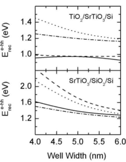
Figure 3 shows the results for electron-heavy hole recombi-nation energy inTiO2/SrTiO3/SiQW (top) andSrTiO3/SiO2/Si QW (bottom), as function of the QW width forSrTiO3(SiO2) layer with thickness of 1.0 nm and 1.5 nm. Solid and dashed lines represent carrier recombination energy including the ef-fects due to image charges.
Dashed dotted and dotted lines represent carrier recom-bination energy without image charges effects. The attrac-tive character of the image potential in the well region of
FIG. 1: ConfinementV(z) =V0(z) +Vim(z)potentials for 50 ˚A wide TiO2/SrTiO3/Si(left) andSrTiO3/SiO2/Si(right). Energy levels and
wave function are also depicted.
FIG. 2: Electron (top) and heavy hole (bottom) ground states wave functions confined in abrupt TiO2/SrTiO3/Si and SrTiO3/SiO2/Si
QWs, with well width of 4 to 6 nm.
TiO2/SrTiO3/Si QW, Fig. 3 (top), decreases the recombina-tion energy (solid and dashed lines), when compared with carrier recombination energy in QW without image charge ef-fect (dashed dotted and dotted lines). The repulsive image potential in the well region ofSrTiO3/SiO2/SiQW, Fig. 3 (bot-tom), increases the recombination energy. TheSrTiO3(SiO2) layer is expressive because it strongly affects the recombina-tion energy of the QWs. Fig. 3 also shows that increasing the thickness of theSrTiO3(SiO2)layer, the recombination en-ergy blue-shift inTiO2/SrTiO3/Siby about 40 meV and in
Brazilian Journal of Physics, vol. 36, no. 2A, June, 2006 349
FIG. 3: Electron-heavy hole recombination energy in (top) TiO2/SrTiO3/Si and (bottom)SrTiO3/SiO2/Si, as a function of the well width andSrTiO3(SiO2)layer with thickness of 1.0 nm (solid
and dashed dotted lines) and 1.5 nm (dashed and dotted lines).
In conclusion, we have studied image charges effects in TiO2/SrTiO3/SiandSrTiO3/SiO2/SiQWs. The image charges related potential structure (sharp and deep) can trap electrons close to theSrTiO3/Siinterfaces. In this system we also ob-served that the attractive character of the image potential in-side of the well region decreases the recombination energy. For SrTiO3/SiO2/Si QW we observed electron confinement only for a 0.9 eV conduction band offset between theSrTiO3 andSilayers. This structure does not have a sharp and deep potential profile due to the repulsive character of the image po-tential that increases the recombination energy, consequently the carrier do not presents an interfacial confinement.
Acknowledgement
T. A. S. Pereira and M. G. Bezerra were supported by Brazilian National Research Council (CNPq). The au-thors also would like to acknowledge the NanoSemiMat #550.015/01-9.
[1] J. Robertson, J. Vac. Sci. Technol. B18, 1785 (2000). [2] S. Migita, S. Sakai, J. Appl. Phys.89,5421 (2001). [3] R. Tsu, Nature364, 19 (1993).
[4] Z. H. Lu, D. J. Lockwood, J. -M. Baribeau, Nature378, 258 (1995).
[5] R. Droopad, Z. Yu, J. Ramdani, L. Hilt, J. Curless, C. Over-gaard, J. L. Edwards, J. Finder, K. Eisenbeiser, J. Wang, J. Wang, V. Kaushik, B-Y Ngyuen, B. Ooms, J. Cryst. Growth 227/228, 936 (2001).
[6] S. A. Chambers, Y. Liang, Z. Yu, R. Droopad, and J. Ramdani, J. Vac. Sci. Technol. A19,934 (2001).
[7] A. C. Tuan, et al., App.Phys. Lett.83, 3734 (2003).
[8] T. A. S. Pereira, E. W. S. Caetano, J. A. K. Freire, V. N. Freire, and G. A. Farias, Brazilian Journal of Physics34, 684 (2004).
[9] J. A. K. Freire,G. A. Farias, and V. N. Freire, Solid State Com-mun.106, 559 (1998).
[10] G. Theodorou, G. Tsegas, P. C. Kelires, E. Kaxiras, Phys. Rev. B60, 11494 (1999); J. R. Chelikowsky and M. Schluter, Phys. Rev. B15, 4020 (1997).
[11] B. Brar, G. D. Wilk, A. C. Seabaugh, Appl. Phys. Lett.69, 2728 (1996).
[12] M. Marques, L. K. Teles, V. Anjos, L. M. R. Scolfaro, J. R. Leite, V. N. Freire, G. A. Farias, E. F. da Silva Jr., Appl. Phys. Lett.82, 3074 (2003).
![TABLE I: Parameters of the materials used in our theoretical calcu- calcu-lations [10-12].](https://thumb-eu.123doks.com/thumbv2/123dok_br/18982254.457473/2.892.481.817.114.332/table-parameters-materials-used-theoretical-calcu-calcu-lations.webp)