Exploiting the Electrical Properties of thin
Films of Semiconducting Polymers
Rob erto M.Faria andO.N. OliveiraJr. InstitutodeFsicadeS~aoCarlos,USP C.P.369,13560-970S~aoCarlos,SP,Brazil
Received 22 May, 1998
A brief review is provided of the ways electrical properties of semiconducting polymers can be exploited. Emphasis is given to the analysis of electrical conductivity data, in particular to the importance of interchain processes that must be considered along with intrachain processes for bulk conductivity. Among the large variety of possible applications of thin lms of semiconducting poly-mers, the focus is placed on recent breakthroughs in producing diodes, eld eect transistors and electroluminescent devices out of these materials. The fabrication of ultrathin lms from semicon-ducting polymers, using the Langmuir-Blodgett and the self-assembly techniques, is discussed to illustrate the importance of processibility issues for any real application including these polymers.
I Introduction
Due to their remarkable intrinsic electrical insulat-ing characteristics, organic polymeric materials have been for a long time the subject of extensive dielec-tric and charge storage studies [1-3]. Elecdielec-trical break-down, charging-discharging mechanisms, thermoelec-tric and radiation eects, and dielecthermoelec-tric relaxation pro-cesses have been investigated from both experimental and theoretical points of view. Insulating polymers are now widely used as insulation in power cables in en-ergy distribution networks, and in dierent types of high accuracy equipment. The contribution of Prof. B. Gross in this area started at the early 70s, when he introduced uorinated polymers as extremely good electrets owing to their large charge storage capacity and remarkable mechanical properties [4]. The com-bination of such properties allowed these polymers to be applied as active membranes in electroacoustic de-vices [5]. Later on the family of polyvinylidene uoride (PVDF) found several applications as piezoelectric and pyroelectric devices, deriving from their ferroelectric ac-tivity [6].
Until the early 1980s, most studies and applications using electrical properties of polymeric materials only exploited their insulating and charge storage capabili-ties. A new turn, both in science and technology, took place in the 1980s with the advent of the conducting and semiconducting polymers [7], with polyacetylene being their foremost representative in the initial studies [8]. Several possible applications have since been suggested
and actually demonstrated in which the polymer is em-ployed not only as a passive, insulating element, but also with an active role, as in microelectronic device components [9].
One major diculty, which is even now a stumbling block for the widespread use of conducting polymers, is fabrication in the required form and shape. The rst conducting polymers produced were almost invariably insoluble and infusible. Over the years, new approaches have been implemented by various research groups in order to overcome the fabrication diculty. Such ap-proaches stem from synthetic chemistry methods [10] with incorporation of side groups that make the poly-mer soluble, new techniques for growing lms electro-chemically[11] and the use of functionalized acids to im-prove solubility in standard organic solvents [12]. These major eorts have now paid o, which is demonstrated by the large number of conducting polymers produced worldwide, some of them commercially available [13].
II Electrical conductivity of
semiconducting polymers
The singular - and most important - property of con-jugated polymers is their electronic conduction along a single chain. Under doping, the conductivity of a poly-meric lm may increase by up to fteen orders of mag-nitude, and the basic phenomenon causing this spec-tacular variation is the appearance of extended states in a chain. This starts with the generation of localized states in the forbidden gap of the one-dimensional elec-tronic structure, which are associated with induced con-formational defects combined with solitons, polarons and/or bipolarons. The electronic properties of these polymeric chains have opened up a new branch of in-vestigation in condensed matter, as well as a new class of materials - the so-called electronic plastics.
Since the bulk structure of organic polymeric lms is surely among the most complicated in condensed mat-ter, obviously the electronic conduction mechanisms in-volved in the charge transport of conducting and semi-conducting polymers are not as simple as described by the band model. In a simple picture one may split the electronic conduction in these materials into two con-tributions: i) along a single molecule and ii) interchain processes. This has been the subject of numerous in-vestigations since the late 1970s. In the following, we present a brief, generalized description of the two pro-cesses.
Figure 1. Two equivalent conformations for trans-polyacetylene.
Theoreticians have been involved in the challenging task of establishing a framework for the single chain conductivity. The rst widely successful model was the SSH model, developed by Su, Schrieer and Heeger
[22,23], in which the electrical conductivity is generated by solitonic defects in polyacetylene chains under dop-ing. Because of its simple chemical structure, the trans-polyacetylene molecule (innite chain) was considered as the prototype of a conjugated molecule for molecu-lar electronic conduction. Since trans-polyacetylene has two equivalent conformations (Fig. 1), the SSH model assumes a topological degenerate ground state [22,23]. The SSH approach involves a tight-binding calcu-lation for a single chain with cyclic boundary condi-tions, and neglects electron-electron interaccondi-tions, with the chain being a sequence of carbon atoms in which -bonds are represented by a spring constant K. The Hamiltonian in the SSH model is then expressed by:
H=, X
n [t
0+ (u
n ,u
n+1)]( c
+ n c
n+1+ c
+ n+1
c n)+
1 2M
X n
p 2 n+
K 2
X n
(u n
,u n+1)
2
: (1)
wherec n+and
c
nare the creation and annihilation op-erators, respectively. The rst sum in the expression is the kinetic energy of-electrons, wheret
0+ (u
n , u
n+1) is the linearized bond length dependence of the transfer integral t
n;n+1 ;u
n is the displacement of the n-carbon atom,t
o is the transfer integral of adjacent atoms whenu
n= 0, and
is the electron-phonon cou-pling constant. The second sum gives the kinetic energy of the lattice, where p
Figure 2. The dispersion relation E(k) versus k for a non-dimerized system leads to a half- lled band. EF is the Fermi energy.
Figure 3. For a dimerized system, a gap appears in theE(k) versuskplot at the Fermi level, the so-called Peierls gap.
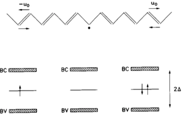
The bond alternation phenomenon (single-double to double-single sequences) in a trans-polyacetylene chain generates an electronic energy level in the mid-gap (see Fig. 4). This energy level, called a soliton, is spread over approximately 14 carbon sites and is ofp
z-orbital nonbonding character. Under strong chemical doping, the number of such states increases signicantly, gener-ating an extended state conguration and consequently increasing the chain conductivity. In any other conju-gated polymer each bond alternation generates a double level in the gap as shown in Fig 5.
Figure 4. A defect, represented by a change in the alterna-tion of the conjugated chain shown in the upper part of the gure, generates an electronic level within the gap. This electronic level is called a soliton. The gap energy is 2, corresponding to the ,
gap. BV and BC are the va-lence and conduction bands, respectively. The gure on the left represents a neutral molecule with spin, the central g-ure corresponds to a spinless positively charged molecule, and the gure on the right a spinless negatively charged molecule.
Figure 5. For conducting polymers other than trans-polyacetylene, a defect in the bond alternation generates a double level in the 2 gap. In the gure, bp
2+and bp
2, stand for the bipolaronic levels while p
+ and p
,stand for the polaronic levels. The gure in the middle represents the unstable exciton.
The levels in the forbidden band enhance the bulk conductivity of these highly disordered polymeric ma-terials. The bulk conductivity also depends strongly on interchain processes, as illustrated in a study of ac con-ductivity of protonated polyaniline [25]. In the PANi structure, the dopant molecules are not uniformly dis-tributed, but agglomerate forming dispersed conduc-tive islands [26]. Nevertheless, it is reasonable to ex-pect that traces of dopant molecules exist in the en-tire structure due to the diusion process. The original (undoped) matrix remains less conductive, with car-rier transport occurring via a hopping mechanismwhich seems to obey the random-free barrier model [27], and is therefore temperature dependent.
c
~
(!) =i!
0
2, i
2(!) !
2(1 ,)
h
0
2, i
2(!) !
i
,(1 + 2) i1(!)
! (2 +)
h
0
2, i
2(!) !
i
,(1,) i1(!)
!
(2)
d where f =! =2, and the indices 1 and 2 refer respec-tively to medium 1, comprising conductive islands with a real conductivity 1, and medium 2 comprising the matrix with real conductivity 2. The dielectric con-stants of medium 1 and 2 are 1 and 2, respectively. The conductive islands are assumed spherical, with being their relative concentration in terms of volume fraction. Since not all the molecules in the conduc-tive islands are strongly doped, is necessarily higher than the doping degree. The conductivity of the ma-trix,2(!), is assumed to occur by hopping in a disor-dered medium, governed by random free-energy barri-ers between the residence sites, and so obeying Dyre's equation [27] .
~
(!) =(0)
i! =min ln(1 +i! =min)
: (3)
min is activated following an Arrhenius process 0e
,Wmin=k T, where
0is a frequency factor andW ithe minimumvalue of the free-energy barriers. ~
D(
!) is es-sentially constant at low frequencies, i.e for! =min << 1, but rises at! =min 1. The physical reason for this is that at low frequencies the carrier has enough time to nd a dicult jump, requiring a high activation en-ergy. For increasing frequencies, the motion becomes more localized in time and the carrier has increasingly lower probability of facing a dicult jump. Hence the activation energy of the process tends to decrease.
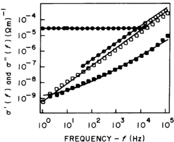
Figures 6 and 7 show both the real and the imagi-nary components,
0(
f) and"(f), of a.c. conductivity measured in PAN lms, with dierent doping degrees and at dierent temperatures, respectively. The con-tinuous curves are the ttings obtained from the model described by the combination of Eqs. (2) and (3). It is important to remark that the Kramers-Kronig rela-tions, in the frequency range employed here, do not fully determine "(f) out of
0(
f) and vice-versa. Related problems, derived from the non-local character of the Kramers-Kronig relations, have already been discussed in the literature [29].
Figure 6. The real and imaginary components, 0 and
", respectively, of the conductivity are plotted against the fre-quency,f, for two degrees of doping of a PAN lm. The real component is represented by full circles (moderately doped) and full squares (weakly doped), while the imaginary com-ponent is represented by empty circles (moderately doped) and empty squares (weakly doped). The measurements were carried out at 300K.
Figure 7. The real and imaginary components, 0 and
The bulk conductivity is an important physical pa-rameter not only because it monitors the doping e-ciency of polymer molecules, which bear charged de-fects in the chains, but mainly because its value di-rectly reects three-dimensional charge delocalization phenomena. The complete conduction process involves the interchain diusion rate, which depends on the in-terchain transfer integralt
? and on the intrachain free time
k [30]. The transfer integral t
? is related to the overlap of the electron wave function of two neighboring molecules and decays exponentially with increasing in-terchain distance. In summary, the successful applica-tion of the phenomenological model of a.c. conductivity is a clear indication that interchain processes must be taken into account when analyzing electrical properties of semiconducting polymers.
Further evidence of the importance of interchain (or interdomain) contribution to the measured electrical conductivity is provided by the analysis of experimental data from ultrathin polymer lms. One should expect that Langmuir-Blodgett (LB) as well as self- assembling (SA) lms made from conducting polymers should dis-play higher conductivity owing to the organized nature of such lms. However, measured d.c. conductivities for these ultrathin lms are consistently lower than for their counterpart, spin-coated or dip- coated lms [31]. The ultrathin lms also contain islands, because of the tendency of conducting polymers to aggregate, and the aggregation in Langmuir monolayers can be probed at the air/water interface using Brewster angle microscopy [32]. The assumption of conducting islands was also employed to explain conductivity data on LB lms of poly(3- hexylthiophene) [33]. The interdomain contri-bution may be the dominant one, because it is likely that any defect or pinholes, inevitable even in high qual-ity, uniform LB lms, may aect the connectivity be-tween domains. This reduces the measured conductiv-ity considerably, whereas for thicker lms connectivconductiv-ity may not be a problem, in spite of the higher number of defects the lms may possess.
III Examples of applications of
semiconducting polymers
Thin lms of weakly and moderately doped conjugated polymers are suitable for some applications as active materials in electronic and photonic devices. Among the wide variety of possible applications that have been reported in the literature, we shall discuss diodes, electroluminescent devices and eld-eect transistors (FETs).
III.1 Diodes
The physical principles as well as the processing re-quirements involved in electronic or photonic devices have as starting point the fabrication and characteriza-tion of a single diode. Two main rectier systems have dominated microelectronics since early years: the p-n junction and Schottky diodes. When semiconducting polymers are employed as the active thin layers of new devices, interface phenomena play a major role, and therefore the study of such phenomena is the rst, fun-damental step in device research. Owing to its simplic-ity, a diode structure is adequate for a rst study, and Schottky-barrier diodes are usually considered. The equation which governs the current across a Schottky interface is given by:
J =J satexp(
eV=nk T) (4)
where n is a factor taken as near unity for an ideal diode. However, in thin lms tunneling in-jection through metal/semiconductor interfaces is of-ten observed. At higher forward biases the cur-rent is limited by the bulk resistance, and in the case of thermionic emission the saturation current is J
sat = A
T
2exp(
eW =k T), where A
is the Richard-son constant, equal to 120 A=K
2cm2, and
W is the barrier height. This has been observed for diodes produced from poly(2-methoxy,5-(2'-ethyl-hexoxy)-1,4-phenylene-vinylene), known simply as MEH-PPV [34]. In fact, several experiments were performed with a thin lm diode of MEH-PPV, from which it could be un-equivocally concluded that both hole and electron in-jection phenomena are dominated by tunneling at low biases, showing a Schottky barrier higher than 17 V. Figure 8 shows that the J ,V characteristic curve of an ITO/MEH- PPV/Ca structure depends on the lm thickness, but it is nearly thickness-independent for an J,E(Eis the electric eld) characteristic curve. The device obeys a Fowler-Nordheim injection mechanism expressed by:
J /E 2exp(
,K =E) (5)
Figure 8. (a) Current density versus bias voltage character-istics for ITO/MEH-PPV/Ca structures of dierent thick-nesses. Full circles - 47.5 nm, Empty squares - 90 nm, Empty circles - 120 nm and Full squares - 210 nm. From ref. [34]. (b) Current density (J) versus electric eld (E) for the struc-tures of (a). These curves are very nearly independent of thickness, as shown in the insert for one particular thickness. From ref. [34].
Another set of interesting experiments were car-ried out with poly(o- methoxyaniline)(POMA) samples doped with HCl on one surface [35]. Figure 9 shows a clear rectication eect, in which the protonated sur-face region, consisting mainly of the conducting emeral-dine salt of poly(o-methoxyaniline) (POMA-ES), most probably acts as the contact injecting holes into the undoped bulk containing the emeraldine base poly(o-methoxyaniline) (POMA-EB). This rectication phe-nomenon is also consistent with the hypothesis that holes are the mobile carriers in the POMA structure. Very similar eects were observed with other dopants
(H3PO4 and toluene sulfonic acid, TSA) and also with polyaniline (PAN) lms [36]. The hole mobility in the POMA bulk was directly obtained from time-of-ight measurements, yielding 310
,4cm2/Vs, which is sim-ilar to that found in poly(p-phenylene vinylene) (PPV) [37]. Apparently, conjugated polymers possess simi-lar carrier mobilities when interchain hopping processes prevail [38].
Figure 9. Current versus bias voltage characteristics for a poly(o-methoxyaniline) sample doped on one surface with HCl, showing rectication. From ref. [35].
III.2 Electroluminescent devices
Fig. 11 for a luminescent diode ITO/MEH- PPV/Ca [34].
Figure 10. Absorption, photoluminescent emission and elec-troluminescent emission curves for PPV at 300K. From ref. [9].
Figure 11. Rectication curve (full circles) of a diode of PPV and the corresponding luminescence curve (empty cir-cles) as a function of the applied voltage. From ref. [34].
Since changes in the polymeric lm, following modi-cation of the polymer itself by chemical synthesis, or of the lm architecture, may cause the luminescent prop-erties to vary widely, the opportunity to tailor the mate-rials for specic applications exists. Thus, for the same polymer family (e.g. PPV and their derivatives) the color of emission may be changed from yellow-greenish to orange [39] to blue [40]. Furthermore, combination of dierent polymers may also vary the emitted color [41]. Many researchers have sought an enhancement in per-formance by employing the polymeric materials in the form of ultrathin lms. A certain degree of molecular control has already been demonstrated in the changes of uorescence properties of SA lms made from PPV [39]. In the latter work, the uorescence emission from PPV
was quenched by building adjacent layers of PPV/C60 (sulfonated fullerene), owing to the non-radiative elec-tron transfer from PPV to C60 [39]. This quench-ing behavior was observed earlier [42] in cast lms of PPV/C60. The novelty [39] was that the uorescence could be recovered if inert spacer layers (say of polyal-lylamine and sulfonated polystyrene (PAH/SPS)) were interposed between PPV and C60 layers. This option is not available in the spin-coated lms.
Using SA lms, it has been possible to build de-vices whose emission wavelengths can be altered and whose eciencies can be enhanced by altering the lm architecture. This was well illustrated by Rubner and collaborators [43,44], which showed that the light out-put of PPV SA lms could be increased by identifying optimized supramolecular architectures that contained PPV/SPS (polystyrene sulfonic acid) and PPV/PMA (polymethacrylic acid) layers. The output could be fur-ther enhanced if passive layers of SPS/PAH (polyally-lamine) were deposited adjacent to the aluminum elec-trode. This example again points to the advantage of employing materials whose properties can be tailored at the molecular level.
III.3 FETs
Here we provide a brief description of the fabri-cation process and characterization of FETs produced from poly(o-methoxyaniline), POMA. We believe that the results and their analysis illustrate the potential of conducting polymers and also the problems to be overcome for the successful application of these mate-rials in devices. Fig 12 shows a eld eect transistor of poly(o-methoxyaniline) (POMA-FET) where a highly doped p-silicon substrate, used as gate electrode, was covered with a thin, thermally grown SiO2 lm. Both source and drain electrodes were made from evaporated gold with a nger shape, with length L and width W. Drain current-voltage characteristic curves (I
D vs V
D), for dierent gate voltages, V
G, are shown in Fig. 13. The drain-source conductivity increases with negative V
Gvalues, indicating a p-type semiconductor as already demonstrated for a POMA lm.
The characteristics of a FET device are usually rep-resented by a plot of the drain currentI
Das a function of the voltage V
D, with the gate voltage V
G as a pa-rameter [45],
I D=
C ox
W =L[(V G
,V th)
V D
,1=2V 2 D]
: (6)
in which, for higher values ofV
I
D ;sat= (
W =2L)C ox(
V G
,V th)
2
: (7)
I
D ;satis the drain current in the saturation regime, V
th is the threshold voltage,V
Gis the gate voltage,
is the carrier mobility, and C
ox is the capacitance per unit area of the oxide layer. The conductivity of the POMA lm is given by = ne, where n is the carrier den-sity and e is the electronic charge. The results of Fig-ure 13 may be tted using = 1:710
,3 cm2 V,1 s,1, V
th=
,7:5 V and= 310
,8,1 cm,1. In comparison with what is found in the literature, the mobility here is high for a conjugated polymer with low conductivity.
Figure 12. Schematic diagram of a eld-eect transistor made from poly(o-methoxyaniline). A strongly p-doped sil-icon was used as gate, covered by a thin layer of SiO2. The drain and source electrodes were made from evaporated gold with a nger shape. A POMA layer is deposited through spin coating on top of this arrangement.
Figure 13. Drain current, ID, versus drain voltage,VD, for a POMA FET and dierent values of gate voltage, VG.
IV
Processing conducting
polymers
In the last two sections, a number of results and ex-amples were described in connection with thin lms of conducting polymers, with no mention of the diculties in producing such lms. We now elaborate on produc-tion diculties which have required intensive work not only in chemical synthesis but also in the engineering of conducting polymers. The focus will be on ultrathin lms, namely Langmuir-Blodgett (LB) [15-18] and self-assembled (SA) lms [18-21], since the requirements for producing these are usually the most stringent. In fact, the interest in these lms appeared owing to the possi-bility of enhancing material properties by some degree of molecular control. This stems from the encouraging results obtained with conducting polymers processed in a number of dierent ways, based on a rich variety of materials and on the immense potential for applica-tions.
In the Langmuir-Blodgett method, a very thin layer of the polymeric material, ideally a monolayer, is spread on an aqueous subphase which can then be transferred onto solid substrates in a layer-by-layer fashion. This method oers precise control over the lm thickness, with ultrathin (nm) lms being produced, and the pos-sibility of tailoring the lm properties by altering the lm architecture. Changes in architecture can be per-formed at two levels, either by modifying the poly-mer backbone or attaching side groups to the chains, and/or in the fabrication of superstructures similar to the semiconductor heterostructures produced by molec-ular beam epitaxy, in which two or more materials are employed.
polymers depend upon experimental conditions such as volume of solution spread, concentration of the spread-ing solution and even speed of barrier compression.
Such dependency arises in most cases from the ten-dency of conducting polymers such as polyaniline and its derivatives to form aggregates [46]. As a conse-quence, optimized experimental conditions for obtain-ing stable monolayers leadobtain-ing to high quality LB lms must be determined. By way of illustration, we men-tion a systematic study [47] in which several mixtures of functionalized acids and organic solvents were tried to render the parent polyaniline soluble, which could then be used to form stable Langmuir monolayers. Stabil-ity and transferabilStabil-ity were only achieved if the parent polyaniline was doped while on the aqueous subphase, requiring the use of low pH subphases [48]. Other approaches which have been employed for producing LB lms from polyanilines involve attaching long alkyl chains [49] or alkoxy groups [50] to the polymer back-bone. The resulting polyanilines are in some cases read-ily soluble in various solvents, thus allowing the forma-tion of LB lms. Yet another method uses mixed mono-layers in which the polymer is co-spread on an aqueous subphase with a lm-forming material such as the am-phiphilic fatty acids [51]. These mixed monolayers are readily transferred, leading to excellent lm uniformity [52].
Incorporation of long alkyl chains into polythio-phene chains has also been extensively used for pro-ducing LB lms [53]. In some cases, the mixed mono-layer approach was also employed, the modied poly-thiophene being spread on an aqueous surface together with fatty acids [54]. Such lms could be doped with NOPF6, and used as the semiconducting element in eld efect transistors (FETs) [33]. Polypyrroles are also extremely promising materials, because of their electrical properties. Producing LB lms from polypyr-role required until very recently very ingenious engi-neering methods, e.g. LB lms have been formed using in situ polymerization [55] or by employing alkyl pyr-role monomers [56]. An exciting new possibility has emerged recently with the advent of soluble polypyr-role [57]. This material is obtained by chemical synthe-sis employing functionalized acids, in a similar fashion to the solubility induced in polyanilines as described above. The fabrication of LB lms from the parent polypyrrole and mixed lms with fatty acids has been demonstrated [58]. The optical properties are very sim-ilar to those obtained with other polypyrrole lms, but
the conductivity is still relatively low, as has been the case for LB lms from other conducting polymers. For the PPV family, processibility is also of extreme impor-tance since PPVs are not soluble in organic solvents. Therefore ultrathin lms must be formed from soluble PPV precursors which are then converted into PPV, usually by thermal treatment [59]. PPV lms have been used in a variety of applications, such as in electrolu-minescent devices [60]. The advantages associated with the LB technology are also applicable to the SA lms, for which molecular control can be achieved [61]. In the SA technique, alternating layers of cationic and an-ionic polymers are adsorbed on a solid substrate [19]. Furthermore, the SA technique has an important ad-vantage in that it does not require sophisticated equip-ment. The LB and SA techniques may be considered as complementary.
Polymers varying from the widely studied polyani-lines and other conducting polymers to various poly-electrolytes have been employed and a number of poten-tial applications have been considered [61]. The most investigated and perhaps the most important one in the foreseeable future is in electroluminescent devices [43,44,62], as discussed in Section III. The actual devel-opment of any real world application is always preceded by systematic studies to establish property-structure re-lationships. For the SA lms, in particular, there are a number of issues to be addressed, starting with the process of adsorption itself. Determining the ideal time period for adsorption of a layer of a given material, and how the adsorption rate varies under dierent ex-perimental conditions are tedious but necessary tasks. Within this rationale, a systematic investigation was carried out on the kinetics of adsorption of a polyani-line derivative (POMA) onto glass substrates [63]. It was found that the adsorption occurs in two steps: a very fast, rst order kinetics process with characteris-tic times of 5 - 10 s, followed by a much slower process (characteristic time of100s), indicative of a Johnson-Mehl-Avrami-type adsorption. These processes corre-spond to nucleation of domains in the rst stage, fol-lowed by domain growth in the second stage, as shown by atomic force microscopy [63].
amount of material adsorbed varying according to a simple Langmuir isotherm. It is also worth stressing that even though the SA technique for conjugated poly-mers was initially entirely based on the electrostatic in-teraction, with adsorption of alternating polycationic and polyanionic layers, it is now possible to build high quality SA layers employing H-bond interactions [39].
V Concluding Remarks
In this paper we have focused on two important as-pects of the exploitation of semiconducting polymers in real world applications, namely the ability to build supramolecular structures from these materials, and the analysis of electrical properties of semiconducting poly-mer lms. Recent breakthroughs in fabrication tech-niques have made it possible to produce ultrathin lms of a variety of semiconducting polymers. However, ow-ing to the rich variety of new materials that can be pro-duced, novel developments in the fabrication of lms are likely to be an important issue for some time to come. With regard to the electrical properties, we have shown that interchain processes must be taken into account when analyzing the bulk electrical conductivity of semi-conducting polymer lms. This was illustrated by the application of a phenomenological model that includes carrier transport via an interchain hopping mechanism. Polyanilines, in addition, were considered as compris-ing conductcompris-ing islands dispersed in a less conductive, undoped matrix. Possible applications of the semicon-ducting polymers were also discussed, by taking specic examples in the fabrication of diodes, eld-eect tran-sistors and electroluminescent devices.
Acknowledgements
The authors are thankful to Dr. R.K. Onmori and C.F.O. Grae for helpful discussions. They are also indebted to FAPESP and CNPq for nancial support.
References
1. G.M. Sessler,Electrets, Topics in Applied Physics Series, Vol. 33 (Springer, Heidelberg, 1987). 2. J. Lewiner, D. Morisseau and C. Alquie (Eds),
Proceedings 8th International Symposium on Electrets, IEEE Catalog. No. 94 CH3443-9, (IEEE, N. York, 1994).
3. R. Gerhard-Multhaupt and A.S. DeReggi (Eds), IEEE Transactions on Dielectrics and Electrical Insulation3, 601 (1996).
4. B. Gross, G.M. Sessler and J.E. West, J. Appl. Phys. 47, 968 (1976).
5. B. Gross, in \Static Electrication", Institute of Physics, London, pp. 33-43 (1971).
6. T. Furukawa, Phase Transitions18, 143 (1989). 7. J.L. Bredas and R. Silbey, Conjugated Polymers,
(Kluwer Academic Publishers, Boston, 1991). 8. C.K. Chiang, J.C.R. Fincher, Y.W. Park, A.J.
Heeger, H. Shirakawa, E.J. Louis, S.C. Gau, A.G. MacDiarmid, Phys. Rev. Lett. 39, 1098 (1977). 9. N.C. Greenham and R.H. Friend, in Solid State
Physics Series, Vol.49, ed. by H. Ehrenreich and F. Spaepen, (Academic Press, San Diego, 1995, pp 1-149).
10. L. Robitaile, J-Y. Bergeron, G. D'Aprano, M. Leclerc and C.L. Callender, Thin Solid Films244, 728 (1994).
11. A.A. Athawale, S.F Patil and B. Deore, Polymer International45, 195 (1998).
12. Y. Cao, P. Smith and A.J. Heeger, Synth, Met. 55-57, 3514 (1993).
13. Y. Cao, G.M. Treacy, P. Smith and A.J. Heeger, Synth. Met. 55-57, 3526 (1993).
14. H.S. Nalwa (Ed.), Handbook of Organic Conduc-tive Molecules and Polymers, Vol. 4, Conductive Polymers: Transport, Photophysics and Applica-tions (John Wiley, N. York, 1997).
15. G.L. Gaines Jr., Insoluble monolayers at Liquid-Gas Interface, (Interscience, New York, 1966). 16. G.G. Roberts,Langmuir-Blodgett Films, (Plenum
Press, New York, 1990).
17. M.C. Petty, Langmuir-Blodgett Films - An In-troduction, (Cambridge University Press, Cam-bridge, 1996).
18. A. Ulman, An Introduction to Ultrathin Organic Films - from Langmuir-Blodgett to Self-Assembly, (Academic Press, New York, 1991).
19. G. Decher, J.D. Hong and J. Schmitt, Thin Solid Films210/211, 831 (1992).
20. Y. Lvov, G. Decher and H. Mohwald, Langmuir 9, 481 (1993).
21. M. Ferreira, J.H. Cheung and M.F. Rubner, Thin Solid Films244, 806 (1994).
22. W.P. Su, J.R. Schrieer and A.J. Heeger, Phys. Rev. Lett. 42, 1689 (1979).
23. W.P. Su, J.R. Schrieer and A.J. Heeger, Phys. Rev. B22, 2099 (1980).
24. R. Peierls, Quantum Theory of Solids, (Oxford University Press, Oxford, 1955).
25. J.M. Ginder, A.F. Richter, A.G. MacDiarmid and A.J. Epstein, Solid State Commun.63, 97 (1987). 26. D. Jeon, J. Kim, M.C. Gallagher and R.F. Willis,
Science256, 1662 (1992).
27. J. C. Dyre, J. Appl Phys. 64, 2456 (1988). 28. C.M. Lepienski, R.M. Faria and G.F. Leal
Fer-reira, Appl. Phys. Lett. 70, 1906 (1997).
30. Z.H. Wang, H.S. Javadi, A. Ray, A.G. MacDi-armid and A.J. Epstein, Phys. Rev. B 42, 5411 (1990).
31. L.H.C. Mattoso, O.N. Oliveira Jr. and M.Ferreira, Conducting Polymers (for Langmuir-Blodgett Film Fabrication), Polymeric Materials Encyclopedia,J.C. Salamone (ed.), Vol. 2C, (CRC Press, Boca Raton, FL, 1432 1996).
32. A. Riul Jr., H. Haas, A. Dhanabalan, M.A. Cotta and O.N. Oliveira Jr., 4o. Congresso Brasileiro de Polmeros, Salvador, Bahia (Brazil) (ABPOL, S~ao Carlos, 1997).
33. E. Punkka, M.F. Rubner, J.D. Hettinger, J.S. Brooks and S.T. Hannahs, Phys. Rev. B, 43, 9076 (1991).
34. I. D. Parker, J. Appl. Phys. 75, 1656 (1994). 35. S. Mergulh~ao, R.M. Faria, G.F. Leal Ferreira and
J. Sworakowski, Chem. Phys. Lett. 269, 489 (1997).
36. R.M. Faria and S. Mergulh~ao, unpublished results 37. M. Takiguchi, D.H. Park, H. Ueno, K. Yoshino
and R. Sugimoto, Synth. Met. 17, 657 (1987). 38. E.M. Conwell, H.Y. Choi and S. Jayadev, Synth.
Met. 49-50, 359 (1992).
39. M. Ferreira, O. Onitsuka, W.B. Stockton and M.F. Rubner, ACS Symposium Series, 672, 437 (1997).
40. Y. Kim, S. Kwon, D. Yoo, M.F. Rubner and M.S. Wrighton, Chem. Mat. 9, 2699 (1997).
41. J.A. Osaheni and S.A. Jeneke, Macromolecules 27, 739 (1994).
42. N.S. Sariciftci, L. Smilowitz, A.H. Heeger and F. Wudl, Science258, 1474 (1992)
43. O. Onitsuka, A.C. Fou, M. Ferreira, B.R. Hsieh and M.F. Rubner, J. Appl. Phys. 80, 4067 (1996). 44. A.C. Fou, O. Onitsuka, M. Ferreira, M.F. Rubner and B.R. Hsieh, J. Appl. Phys. 79, 7501 (1996). 45. S. M. Sze,Physics of Semiconductor Devices,
(Wi-ley, N. York, 1981).
46. S. Paddeu, M. K. Ram and C. Nicolini, J. Phys. Chem. B.101, 4759 (1997).
47. A. Riul Jr., L.H.C. Mattoso, G.D. Telles, P.S.P. Herrmann, L.A. Colnago, N.A. Parizotto, V. Baranauskas, R.M. Faria and O.N. Oliveira Jr.,
Thin Solid Films284-285, 177 (1996).
48. A. Riul Jr. L.H.C. Mattoso, S.V. Mello, G.D. Telles and O.N. Oliveira Jr., Synth. Met. 71, 2067 (1995).
49. M. Ando, Y. Watanabe, T. Iyoda, K. Honda and T. Shimidzu, Thin Solid Films179, 225 (1989). 50. L.H.C. Mattoso, S.V. Mello, A. Riul Jr., O.N.
Oliveira Jr. and R.M. Faria, Thin Solid Films 244, 714 (1994).
51. A. Dhanabalan, R.B. Dabke, S.N. Datta, N. Pras-anth Kumar, S.S. Major, S.S. Talwar, A. Q. Con-tractor, Thin Solid Films295, 255 (1997). 52. (a) A. Dhanabalan, A. Riul Jr., L.H.C. Mattoso
and O.N. Oliveira Jr., Langmuir13, 4882 (1997). (b) A. Dhanabalan, A. Riul Jr. and O.N. Oliveira Jr., Supramolecular Sci.,5, 75-81 (1998).
53. I. Watanabe, K. Hong and M.F. Rubner, Lang-muir6, 1164 (1990).
54. A. Pawlicka, R.M. Faria, M. Yonashiro, S.V. Canevarolo, Jr. and O.N. Oliveira, Jr., Thin Solid Films244, 723 (1994).
55. T. Shimidzu, T. Iyoda, M. Ando, A. Ohtani, T. Kaneko and K. Honda, Thin Solid Films160, 67 (1988).
56. K. Hong and M.F. Rubner, Thin Solid Films179, 215 (1989).
57. J.Y. Lee, D.Y. Kim, C.Y. Kim, Synth. Met. 74, 103 (1995).
58. A. Dhanabalan, S.V. Mello and O.N. Oliveira Jr., Macromolecules31, 1827 (1998).
59. D.D.C. Bradley and R.H. Friend, J. Phys. C: Con-dens. Matt. 1, 3671 (1989).
60. Y.Q. Liu, Q.L. Li, Y. Xu, X.Z. Jiang and D.B. Zhu, Synth. Met. 85, 1279 (1997).
61. G. Decher, Science277, 1232 (1997).
62. R. Osterbacka, A.J. Pal, K.M. Kallman and H. Stubb, J. Appl. Phys. 83, 1748 (1998).
63. M. Raposo, R.S. Pontes, L.H.C. Mattoso, Macro-molecules30, 6095 (1997).
64. L.H.C. Mattoso, L.G. Patterno, S.P. Campana and O.N. Oliveira Jr., Synth. Met. 84, 123 (1997).


![Fig. 11 for a luminescent diode ITO/MEH- PPV/Ca [34].](https://thumb-eu.123doks.com/thumbv2/123dok_br/18978681.456225/7.918.110.461.147.418/fig-luminescent-diode-ito-meh-ppv-ca.webp)

