Printed in Brazil - ©2007 Sociedade Brasileira de Química 0103 - 5053 $6.00+0.00
A
r
t
ic
le
A
r
t
ic
le
A
r
t
ic
le
A
r
t
ic
le
A
r
t
ic
le
*e-mail: [email protected]
#Present Address: Instituto de Química, Universidade Estadual de Campinas,
CP 6154, 13083-970, Campinas-SP, Brazil
Retention of Copper(II) Metal Ions in a Silicon-Glass Microfluidic Device
José A. Fracassi da Silva,*,#,a Claudimir L. do Lagob and Rogerio Furlanc
a
Laboratório de Sistemas Integráveis, Escola Politécnica, Universidade de São Paulo, Av. Prof. Luciano Gualberto Trav. 3, nº 158, 05508-900 São Paulo-SP, Brazil
b
Instituto de Química, Universidade de São Paulo, Av. Prof. Lineu Prestes 748, 05508-900 São Paulo-SP, Brazil
c
University of Puerto Rico at Humacao, Department of Physics and Electronics, CUH Station, 100 908 RD, PR, 00791, Humacao, Puerto Rico
Neste trabalho é descrita a construção de um microssistema em silício para retenção de íons cobre(II). Processo fotolitográfico convencional foi empregado para transferir o padrão de microcanais para o substrato de silício. Utilizando corrosão por íons reativos (RIE) com plasma de SF6, foram produzidos canais de 50 µm de largura e 10 µm de profundidade. Os canais foram selados com vidro de borossilicato utilizando-se a técnica de soldagem anódica. Para promover a retenção dos íons cobre(II), a superfície dos canais foi modificada através de reação de silanização com N-(β-aminoetil)-γ-aminopropiltrimetóxisilano. Os íons cobre(II) foram detectados amperometricamente na saída do canal utilizando-se um eletrodo de ouro. Os íons cobre(II) foram eluídos com HCl 50 mmol L-1 em um sistema micro-FIA com fluxo de 100 µL min-1. A reprodutibilidade em termos de área e altura do pico foram de 4,6 % e 10 %, respectivamente, para três injeções consecutivas de 600 µL de solução de cobre(II) 10 µmol L-1.
This work describes the construction of a silicon microchip for retention of copper(II) metal ions. Conventional photolithographic process was applied to transfer the generated pattern to silicon wafers. Using Reactive Ion Etching (RIE), SF6 based, channels 50 µm wide and 10 µm deep were produced. The channels were sealed with borosilicate glass using anodic bonding process. The surface of the channels were modified with N-(β-aminoethyl)-γ -aminopropyl-trimetoxysilane through a silanization reaction to promote the adsorption of copper(II) ions. An amperometric detector was placed at the microchip outlet and copper(II) ions were detected by a gold electrode at 0 V (against Ag/AgCl(KCl sat.) reference electrode). Copper(II) ions were retained and eluted with HCl 50 µmol L-1 in a micro-flow system at a flow rate about 100 µL min-1. Reproducibility in the peak area and height were about 4.6 % and 10 %, respectively, for three consecutive injections of 600 µL of 10 µmol L–1 copper(II) sample.
Keywords: microchip, sample treatment, copper ions, amperometric detection, silicon
Introduction
It is noticeable the tendency of miniaturization of analytical techniques and systems. After almost two decades of intense development, this tendency has proven not to be a fashion, and actually many analytical devices can be found in the market.
It was in the beginning of the 90´s that Manz and coleagues demonstrated in a seminal paper the viability
of the integration of analytical steps onto a single substract,1
called Micro Total Analysis Systems (µTAS) or simply microchip.1-4
After those pioneering works, many efforts have been undertaken to integrate several steps of analysis in a single microchip. There are numerous examples of micro-analytical systems that cover many applications and processes, such as pumping, mixing and diluting, precolumn and postcolumn reactors, injectors, filters, preconcentrators, cell sorters, detectors, and so on.5-8
Considering that in most situations the sample pretreatment is crucial for the success of the analysis,9
the analytical steps but also the connection with the macroscopic world.
Although glass or quartz, and more recently polymers, are the most commonly used materials for the fabrication of micro-analytical systems, there are many examples of devices built in silicon. In fact, the protocols for the microfabrication in silicon are very well established, as a result of several years of development of the microelectronic industry. To illustrate, applications can be found for conventional
liquid chromatography,2 ion chromatography,10
microchip electrophoresis,11,12 DNA amplification,13
protein identification,14 filter chamber15 or substrate for
bead immobilization,16,17 asymmetric catalysis,18 and
construction of valves19 and injectors.20
Although examples of microdevices that deal with metal ion liquid-liquid extraction21 or electrophoretic
separation of metal complexes22 can be found in the
literature, according to the knowledge of the authors there are not such examples of metal ions retention in such microchip devices using complex formation strategies. Through this kind of strategy high selectivity can be achieved by changing the characteristics of the stationary phase, or more specifically, the chelating agent immobilized to the channels surfaces.
In this work a silicon microchip for metal ions retention is proposed. The microchip was constructed using lithographic protocol to pattern channels in a silicon substrate. The silicon substrate was anodicaly bonded against a borosilicate glass in order to seal the microchannels. The usefulness of the device is demonstrated by the retention of copper(II) ions adsorbed to the modified surface followed by amperometric detection at the gold microelectrode placed at the microchip outlet.
Experimental
Reagents
All the chemicals were of analytical grade. Potassium chloride, hydrochloric acid, nitric acid, copper(II) sulfate, toluene, chloroform, and methanol were obtained from
Merck (Darmstadt, Germany). N-(β
-Aminoethyl)-γ-aminopropyltrimetoxysilane (AEAPTS) was obtained
from Pierce (Rockford, Illinois, USA). The reagents for the lithographic process were electronic grade and were obtained from J. T. Baker (Phillipsburg, NJ, USA). All the electrolytes and standard solutions were prepared by dissolving the reagents or diluting stock solutions in deionized water (Barnstead/Thermolyne, Dubuque, IA, USA).
Microchip fabrication and characterization
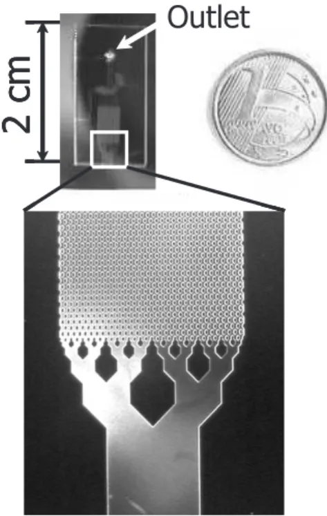
The microchip pattern presented in Figure 1 was generated using CAD and the mask was photo-plotted. The maximum resolution that can be obtained with this type of mask is about 40 µm. The pattern was transferred to <100> silicon wafers (p-type, 10-20 Ωcm, 380 µm thick), which were previously cleaned (RCA standard process)23 and
thermally oxidized (ca. 1 µm, T = 1150 °C, O2, 2 L min-1,
20 hours + N2, 2 L min-1, 30 min). The lithographic process
used positive photoresist (ONPR800, Tokyo Ohka Co., Japan) and the exposed silicon oxide was etched using a buffered oxide etching solution (BOE), which is a mixture of HF 49 % and NH4F 40 % (1:6, v/v) solutions. The wafers were loaded in the reactive ion etcher (home built) and processed using SF6 for 10 minutes (50 W of RF power, 20 Pa, 25 sccm flow). After silicon oxide was completely removed with BOE, the wafers were cut, RCA cleaned, and the small pieces were sealed with glass (Pyrex 7740, 2 mm thick) using an anodic bonding process (380 °C, 800V). A 0.25 mm hole was drilled in the glass before the sealing to serve as a fluid outlet. A silicone tube was glued at the side of the device, by using acetic silicone glue (General Electric, Waterford, NY, USA), defining the inlet.
The channels surfaces were modified according to the protocol proposed by de Jesus et al.24 The channels were
filled with a solution of 5 % AEAPTS in dry toluene for
30 minutes, washed with dry toluene, chloroform, and methanol, in this sequence. Finally, the microchip was left in an oven at 80 ºC for 24 hours to complete the cure of the deposited film.
In order to perform infrared characterization of the film, the same immobilization procedure was done with pieces of silicon wafers. In this case, the dimensions of the wafers were about 2 cm2. For the control sliver, the
whole immobilization procedure was conducted, except for the inclusion of the AEAPTS reagent. Fourier Transform Infrared (FTIR) spectra were obtained using a FTS-40 spectrophotometer (Bio-Rad, Hercules, CA, USA). Additional data concerning the characterization of the deposited film can be obtained elsewhere.25 Briefly, 4 cm2
control and surface modified silicon pieces were immersed on 2 mL of 50 mmol L-1 copper(II) aqueous solution. After
90 minutes, the wafers were washed with deionized water, dried under nitrogen, and 2 mL of a solution containing 50 mmol L-1 ethylenediaminetetraacetic acid (EDTA) was
put in contact with the pieces in order to promote the removal of the copper(II) adsorbed into the surface through complexation. After 60 minutes, the aliquots were taken to be analyzed by potentiometric stripping with a potential and deposition time of 0 V and 120 s, respectively, using an AutoLab PGStat 20 (EchoChimie). Data analysis showed that at least 2-fold increase in peak height was obtained for the solution in contact with the modified surface, when comparison with the control.
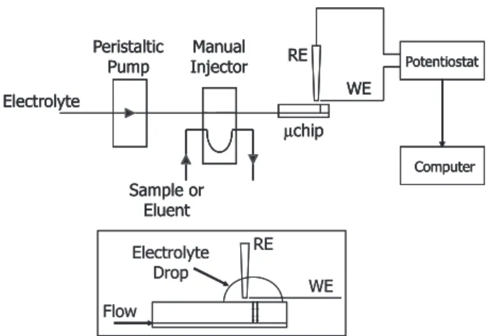
Micro-Flow Injection Analysis
Figure 2 shows the experimental setup for the micro-flow injection analysis (µFIA) experiments. A peristaltic pump (model 7331-10, Ismatec, Switzerland), operating at 100 µL min-1, delivered the fluids to the microchip inlet.
KCl 50 mmol L-1 was used as the carrier electrolyte. Using
a manual injector, copper(II) sample or eluent (50 mmol L-1 HCl) solutions were inserted into the flow. The volume
of the sample loop was 600 µL.
Amperometric detection was performed using a two-electrode cell configuration, as shown in the detail of Figure 2. The electrolyte drop formed at the microchip outlet assured the electrolytic contact between working and reference electrodes. Gold working electrodes were obtained from recordable compact discs (CD-R), and prepared according to Angnes and coworkers.26-28 Briefly,
the CD-R protective coating was removed with nitric acid, and a piece about 0.5 × 4 cm was cut using scissors. Nitrocellulose resin was applied to the gold surface to define the detection window (about 4 mm2) and the electric
contact pad. The electrical contact was achieved by putting
together the exposed gold surface and a piece of wire and firmly wrapping both with Teflon (plumbing) tape.28 A
miniature Ag/AgCl (KCl saturated) electrode provided a reference. The electrochemical cell was connected to a Model 400 electrochemical detector (EG&G Princeton Applied Research, Princeton, NJ, USA). The output current signals were acquired using a multifunction interface card (PCL 711, Advantech, Taipei, Taiwan) and a Pentium® II 233 MHz microcomputer. Data acquisition software was written in Delphi 5.0 (Borland Software, Scotts Valley, CA, USA). The copper(II) reduction current was monitored at 0 V applied to the working electrode.
Results and Discussion
The microchip design was based on the previous work of He et al.29 The basic concept entails the consecutive
splitting of the flow, by reducing the channel to a half of the original width. In the present case, the 1.6 mm inlet channel is divided until it reaches 50 µm in width. The divided flow is then distributed along identical units before it reaches the outlet confluence. This procedure not only guarantees the uniform distribution of the material, but also enhances the surface to volume ratio. It can be calculated that the volume of the region formed by the 50
µm channel ensemble is about 100 nL, assuming that the channel walls are perfectly perpendicular. Due to isotropic plasma etching corrosion, the channel walls appear non-perpendicular, which implies a slightly larger volume for this region. Figure 3 shows the channel profile obtained using the conditions mentioned in the experimental section.
Figure 4 shows FTIR spectra for both silicon dioxide and silicon dioxide with the immobilized film wafers. The Figure 2. Micro-flow with amperometric detection setup. Electrolyte and eluent were KCl 50 mmol L-1 and HCl 50 mmol L-1, respectively. The sample
loop was 600 µL and the flow rate was 100 µL min–1; RE, reference
spectrum for the silicon dioxide (Figure 4a) is the expected for a thermally grown oxide,30 presenting strong absorption
bands in 460 cm–1 (Si-O-Si bending), 800 cm-1 (O-Si-O
bending), and 1080 cm-1 (Si-O stretching). A characteristic
shoulder can be observed at 1254 cm-1. A weak band at
3640 cm-1 can be attributed to the presence of silanol groups
(Si-OH). Additional bands at 2800 and 3000 cm 1 can be
found in the spectrum of the modified surface (Figure 4b), and can be respectively attributed to C-H and N-H stretching. Other bands can be seen between 1300 and 1800 cm-1. In
this way, the FTIR spectrum offers a good confirmation of the presence of the immobilized AEAPS film.
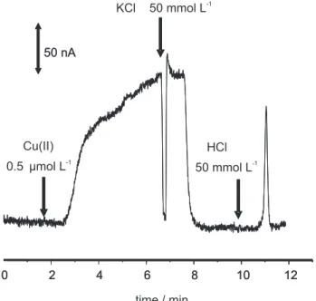
Figure 5 shows an example of the whole procedure for copper(II) retention using the microchip. In this experiment the copper(II) sample, eluent, and electrolyte were directly inserted in the flow. Before sample introduction, the microchip and connections were filled with 50 mmol L-1 KCl electrolyte. Additionally, a drop
was created at the detector point to make the electrical
contact between working and reference electrodes, and the data acquisition was turned on (t=0 in Figure 5). At approximately 1.5 min, 0.5 µmol L-1 copper(II) sample
solution was introduced into the flow. After 1 minute, the copper(II) reached the working electrode and the current started to rise. The copper(II) sample was passed into the microchip for approximately 7 minutes, when the flow was stopped and KCl 50 mmol L-1 electrolyte was inserted
into the flow. The microchip was washed with the electrolyte for 4 minutes, removing the copper(II) ions that were not retained by the bonded AEAPS. Finally, 50 mmol L-1 HCl eluent was introduced (at 10 minutes in
Figure 5) and a peak, related to the copper(II) that was retained, was observed.
As reported by Jesus et al.,24 N-(β -Aminoethyl)-γ-aminopropyl group (AEAPS) presents favorable stability constant for copper(II), but also exhibit selectivity for zinc(II), cobalt(II), nickel(II) and magnesium(II). Although these ions are possible interfering species, the potential applied to the gold electrode is not enough for the reduction of these ions. In this way, good selectivity for the device is expected. But is worthwhile to remember that high concentration of interfering species could shift the equilibrium for the complex formation and remove the linked copper(II) from the immobilized film. Also, the pH of the medium must be controlled to avoid the AEAPS protonation.
Figure 3. Microchannel profile obtained with scanning electron micros-copy (SEM) of a 50 µm channel.
Figure 4. Fourier transform infrared spectra of silicon slivers. (a) Control sliver; (b) piece of silicon after the immobilization procedure.
Figure 5. Signal obtained in the retention of copper(II) ions. At approxi-mately 1.5 min (a) 0.5 µmol L-1 copper(II) solution was injected and the
amperometric current slowly started to rise (retention step); at 7 min (b), KCl 50 mmol L-1 solution was injected into the microchip (washing step)
and the baseline current value was reestablished; at 10 min (c) HCl 50 mmol L-1 acting as eluent was injected and a peak related to the retained
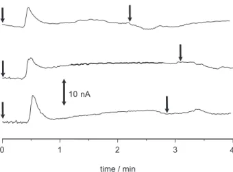
Figure 6 shows three consecutives experiments carried out under the same flow conditions of Figure 5. A manual injector was used with a sample loop of 600 µL for the introduction of both the samples and eluent. Only the elution step is shown in Figure 6. In these experiments, the sample was copper(II) 10 µmol L-1, that corresponds
to 6 nmol of copper(II) ions, and the eluent was again 50 mmol L-1 HCl. For each sample introduction, two elution
steps were performed, as indicated by the arrows in Figure 6. It can be noted that a slight signal is observed for the second elution step, which indicates that complete copper(II) removal was not reached. The reproducibility was about 4.6 % and 10 % in peak area and height, respectively.
Thus, complexation strategies are an attractive alternative for selective binding of metal ions in micro total analysis systems (µ-TAS). Here, the selected ligand was appropriate for copper ions retention, but other functional groups can also be immobilized to enhance the scope of applications.
Conclusions
A procedure for the construction of microchips in glass and silicon was established, for the retention of copper(II) ions. The use of photo-plotter masks reduces the costs of the devices, in detriment of the resolution achieved. Using photo-plotter masks, the minimum channel width is about 40 µm. Under the used experimental conditions, SF6 based plasma etching, operating in the RIE mode, produces microchannels 10 µm deep.
Copper(II) metal ions could be adsorbed into the microchip, and promptly detected using an amperometric Figure 6. Repeatability of the signal for three consecutive injections. The sample was 10 µmol L-1 copper(II), and the elution step was performed
twice. The arrows indicate the exact time the eluent was injected.
detector with a inexpensive gold microelectrode manufactured from CD-Rs. The analysis steps –washing, retention, and elution– were not optimized, but the total analysis time took about 5 minutes using 100 µL min-1
flow rate. Additionally, the sample could be easily manipulated by using an external injector and micro-flow setup. For the case of more diluted samples, the sample loop can also be augmented. Allied to the retention effect, which could be used for preconcentration purposes, this microchip system can also be used as a filter, by cleaning sample matrices and retaining undesirable components. Finally, the integration of the amperometric detector could be conducted through additional steps of metal deposition during the fabrication of the micro-device, but this was out of the scope of the current work.
Acknowledgments
The authors would like to thank Fundação de Amparo à Pesquisa do Estado de São Paulo (FAPESP), and NSF-DMR-0353730.
References
1. Manz, A.; Graber, N.; Widmer, H. M.; Sens. Actuators, B1990, 1, 244.
2. Manz, A.; Miyahara, Y.; Miura, J.; Watanabe, V.; Miyagi, H.; Sato, K.; Sens. Actuators, B1990, 1, 249.
3. Manz, A.; Harrison, D. J.; Verpoorte, E. M. J.; Fettinger, J. C.; Ludi, H.; Widmer, H. M.; Chimia1991, 45, 103.
4. Manz, A.; Harrison, D. J.; Verpoorte, E. M. J.; Fettinger, J. C.; Paulus, A.; Ludi, H.; Widmer, H. M.; J. Chromatogr.1992, 593, 253.
5. Figeys, D.; Pinto, D.; Anal. Chem.2000, 72, 330A.
6. Reyes, D. R.; Iossifidis, D.; Auroux, P.-A.; Manz, A.; Anal. Chem. 2002, 74, 2623.
7. Auroux, P. -A.; Iossifidis, D.; Reyes, D. R.; Manz, A.; Anal. Chem.2002, 74, 2637.
8. Vilkner, T.; Janasek, D.; Manz, A.; Anal. Chem.2004, 76, 3373. 9. Lichtenberg, J.; de Rooij, N. F.; Verpoorte, E.; Talanta2002,
56, 233.
10. Kang, Q.; Golubovic, N. C.; Pinto, N. G.; Henderson, H. T.; Chem. Eng. Sci.2001, 56, 3409.
11. Harrison, D. J.; Glavina, P. G.; Manz, A.; Sens. Actuators, B 1993, 10, 107.
12. Fintschenko, Y.; van der Berg, A.; J. Chromatogr., A1998, 819, 3.
13. Lee, T. M. H.; Hsing, I.-M.; Lao, A. I. K.; Carles, M. C.; Anal. Chem.2000, 72, 4242.
15. Andersson, H.; van der Wijngaart, W.; Enoksson, P.; Stemme, G.; Sens. Actuators, B2000, 67, 203.
16. Andersson, H.; Jönsson, C.; Moberg, C.; Stemme, G.; Electrophoresis2001, 22, 3876.
17. Andersson, H.; Griss, P.; Stemme, G.; Sens. Actuators, B2002, 84, 290.
18. Andersson, H.; Jönsson, C.; Moberg, C.; Stemme, G.; Sens. Actuators, B2001, 79, 78.
19. Andersson, H.; van der Wijngaart, W.; Griss, P.; Niklaus, F.; Stemme, G.; Sens. Actuators, B2001, 75, 136.
20. van der Moolen, J. N.; Poppe, H.; Smit, H. C.; Anal. Chem. 1997, 69, 4220.
21. Minagawa, T.; Tokeshib, M.; Kitamori, T.; Lab Chip2001, 1, 72.
22. Lua, Q.; Collins, G. E.; Analyst2001, 126, 429.
23. Madou, M.; Fundamentals of Microfabrication, CRC Press: New York, 1997, ch. 1.
24. de Jesus, D. P.; Neves, C. A.; do Lago, C. L.; J. Braz. Chem. Soc.2001, 12, 123.
25. Fracassi da Silva, J. A.; Furlan, R.; Proceedings of the Second MIT Conference on Computational Fluid and Solid Mechanics, Cambridge, MA, USA, 2003.
26. Angnes, L.; Richter, E. M.; Augelli, M. A.; Kume, G. H.; Anal. Chem.2000, 72, 5503.
27. Richter, E. M.; Augelli, M. A.; Kume, G. H.; Mioshi, R. N.; Angnes, L.; Fresenius J. Anal. Chem.2000, 366, 444. 28. Richter, E. M.; Augelli, M. A.; Magarotto, S.; Angnes, L.;
Electroanalysis2001, 13, 760.
29. He, B.; Tait, N.; Regnier, F.; Anal. Chem.1998, 70, 3790. 30. Lau, W. S.; Infrared Characterization for Microelectronics,
Word Scientific Publishing Co.: Singapure, 1999.
Received: January 4, 2007 Published on the web: December 10, 2007