João Ricardo Carvalho Magalhães de Carvalho
Design of a CMOS Amplifier for Breast
Cancer Detection
Dissertação para obtenção do Grau de Mestre em Engenharia Eletrotécnica e Computadores
Orientador: Prof. Doutor Luis Augusto Bica Gomes de
Oliveira, FCT-UNL
Presidente: Júri:
Prof. Doutor Pedro Miguel Ribeiro Pereira Arguente: Prof. Doutor João Pedro Abreu de Oliveira
Vogal: Prof. Doutor Luis Augusto Bica Gomes de Oliveira Licenciado em ciências de engenharia eletrotécnica
e computadores
Design of a CMOS Amplifier for Breast Cancer Detection
Copyright © João Ricardo Carvalho Magalhães de Carvalho, Faculdade de Ciências e Tecnologia, Universidade Nova de Lisboa.
Acknowledgments
First I would like to thank my parents who have always been there for me, then I would like to thank professor Luis Oliveira for all the support and patience shown during this project.
Resumo
Faculdade de Ciências e Tecnologia
Departamento de Engenharia Electrotécnica e de Computadores Mestrado Integrado em Engenharia Electrotécnica e de Computadores
por João Ricardo Carvalho Magalhães de Carvalho
Nos detectores de radiação como o Positron tomography (PET), são utilizados amplificadores de transimpedância (TIA), que têm a função de transformar um sinal de corrente produzido por um fotodetector, num sinal de tensão com uma amplitude e forma desejada.
O amplificador de transimpedância deve ter o menor ruido possível, de forma a maximizar o sinal produzido. Nesta dissertação é proposta uma topologia de circuito onde é acrescentado um ramo auxiliar a entrada do conhecido TIA de feedback. No ramo auxiliar um bloco de transcondutância diferencial é utilizado para converter um sinal de entrada de tensão num sinal de corrente. Este sinal de corrente é em seguida convertida num sinal de tensão por um segundo amplificador de feedback, complementar ao primeiro, este sinal tem a mesma amplitude do produzido pelo ramo principal mas esta 180º fora de fase. Com este circuito o sinal de entrada do TIA aparece na saída como diferencial indo-se tirar partido deste facto para se tentar reduzir o ruido.
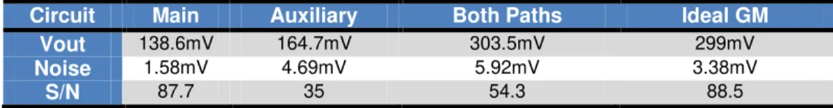
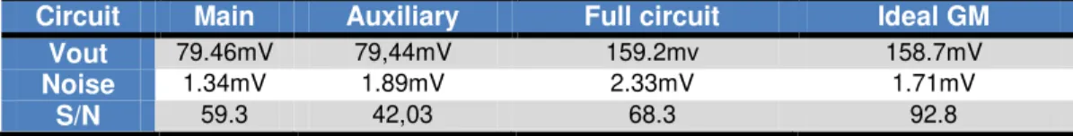
A topologia proposta é testada com dois dispositivos diferentes, o Foto díodo avalanche (APD), e o Fotomultiplicador de Sílico (SIPM). Das simulações concluímos que quando utilizamos o SIPM com Rx=20kΩ e Cx=50fF a relação sinal ruido aumenta, passando de 59 quando se usa apenas o feedback TIA, para 68.3 quando se utiliza o ramo auxiliar.
Os valores foram obtidos com um consumo total do circuito de 4.82mW. Apesar da relação sinal ruido ter melhorado no caso do SIPM, esta vem com um custo no consume total de energia.
Palavras chave
Abstract
Faculdade de Ciências e Tecnologia
Departamento de Engenharia Electrotécnica e de Computadores Mestrado Integrado em Engenharia Electrotécnica e de Computadores
by João Ricardo Carvalho Magalhães de Carvalho
A transimpedance amplifier (TIA) is used, in radiation detectors like the positron emission tomography(PET), to transform the current pulse produced by a photo-sensitive device into an output voltage pulse with a desired amplitude and shape.
The TIA must have the lowest noise possible to maximize the output. To achieve a low noise, a circuit topology is proposed where an auxiliary path is added to the feedback TIA input, In this auxiliary path a differential transconductance block is used to transform the node voltage in to a current, this current is then converted to a voltage pulse by a second feedback TIA complementary to the first one, with the same amplitude but 180º out of phase with the first feedback TIA. With this circuit the input signal of the TIA appears differential at the output, this is used to try an reduced the circuit noise.
The circuit is tested with two different devices, the Avalanche photodiodes (APD) and the Silicon photomultiplier (SIPMs). From the simulations we find that when using s SIPM with Rx=20kΩ and Cx=50fF the signal to noise ratio is increased from 59 when using only one feedback TIA to 68.3 when we use an auxiliary path in conjunction with the feedback TIA.
This values where achieved with a total power consumption of 4.82mv. While the signal to noise ratio in the case of the SIPM is increased with some penalty in power consumption.
Keywords
Contents
Acknowledgments ... v
Resumo ... vii
Abstract ... ix
Chapter 1 Introduction ...1
1.1 Motivation ...1
1.2 Objectives ...2
1.3 Thesis Organization...3
1.4 Contributions ...3
Chapter 2 Photon detection ...5
2.1 Basics ...5
2.2.1-Avalanche Photodiodes (APD) ...6
2.2.1.1- Linear Mode ...6
2.2.1.2- Geiger mode ...6
2.2.2-Silicon Photomultipliers (SIPM) ...7
Chapter 3 Noise ...9
3.1 Thermal noise ...9
3.2 Flicker Noise ...11
3.3 Noise Cancellation...11
Chapter 4 Single stage MOS Amplifiers ...13
4.1 Common Source Stage ...13
4.1.1 Low frequency model neglecting ...13
4.1.2 Low frequency model with ...14
4.2 Common Gate Stage ...15
4.2.1 Low frequency model neglecting ...15
4.2.2 Low frequency model with ...17
Chapter 5 Transimpedance Amplifiers ...19
5.1 Feedback TIA ...19
5.1.1 Transimpedance function ...20
5.1.2 Noise Analysis ...22
5.2 Common Gate TIA...26
5.2.1 Transimpedance Function ...26
5.2.2 Noise Analysis ...28
5.3 Regulated Common Gate ...31
5.3.1 Transimpedance Function ...31
5.3.2 Noise Analysis ...32
6.1 Feedback TIA with Auxiliary Path ...37
6.2 transfer function ...40
6.3 Noise Function ...41
6.3.1 Main path noise ...42
6.3.2 Auxiliary path noise ...43
6.4 Simulation result ...45
6.4.1 Simulation Setup ...45
6.4.2 Using an APD at the input ...47
6.4.3 Using an SIPM at the input ...53
6.4.4 Comparing APD with SIPM...58
Chapter 7 Conclusions ...61
APPENDIX A1 ...63
Noise in Second-Order Networks ...63
APPENDIX B1 ...65
Optimization of a Folded-Cascode OTA Using Mathcad ...65
List of Figures
Figure. 1.1 - Radiation Detector ...2
Figure. 1.2- TIA with input current pulse id and output pulse v0 ...2
Figure. 2.1 - p-n photodiode ...5
Figure. 2.2- Current Pulse ...6
Figure. 2.3- APD simplified model ...7
Figure. 2.4- Simplified SiPM structure ...7
Figure. 3.1- Thermal noise resistor model ...10
Figure. 3.2- MOSFET thermal noise model ...10
Figure. 3.3- Noise cancelling theory using. ...12
Figure. 3.4- Noise figure in relation with path gain. ...12
Figure. 4.1- Common Source amplifier with resistive Load ...13
Figure. 4.2- Small-signal model of the Common-Source amplifier without r0 ...14
Figure. 4.3- Small-signal model of the common-source stage with ...14
Figure. 4.4- Common Gate With Resistive Load ...15
Figure. 4.5- Small signal model of the common-gate amplifier without r0 ...15
Figure. 4.6- Small signal model input impedance without r0 ...16
Figure. 4.7- Small signal of the common-gate amplifier with r0 ...17
Figure. 4.8- Small signal model input impedance with r0 ...18
Figure. 5.1- Feedback TIA ...19
Figure. 5.2- Feedback with a VCVS ...21
Figure. 5.3- Feedback TIA noise sources ...22
Figure. 5.4- Feedback TIA resistor noise ...24
Figure. 5.5- Common Gate TIA ...26
Figure. 5.6- Common-Gate with a voltage post-amplifier ...27
Figure. 5.7- Common Gate TIA noise sources ...28
Figure. 5.8- Small signal model of the CG with noise source ...29
Figure. 5.9- Regulated Common Gate ...31
Figure. 5.10- RCG TIA incremental circuit with noise sources. ...33
Figure. 5.11- Small signal model of the RCG with noise sources ...33
Figure. 6.1- Proposed circuit. ...38
Figure. 6.2- Class-AB CMOS inverter ...38
Figure. 6.3- Complete Transconductance element of the auxiliary path ...39
Figure. 6.4- Inverter noise contribution to the main path ...41
Figure. 6.5- Full circuit noise sources ...41
Figure. 6.6- Feedback TIA with GM noise ...43
Figure. 6.7- Simplified Folded Cascode without polarizing circuit...45
Figure. 6.8- Input and output of the GM block ...47
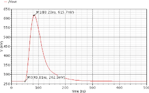
Figure. 6.9- Vin and Vout of the GM with an APD ...48
Figure. 6.10- Vout of the MAIN and AUXILIARY path with an APD...48
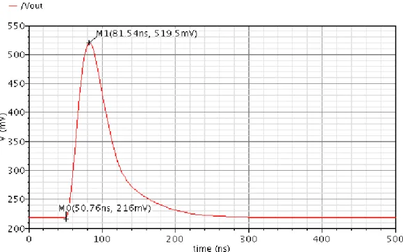
Figure. 6.11- Vout of the full circuit With an APD as the input ...49
Figure. 6.12- Vout of full circuit when using 83k/100f ...51
Figure. 6.13- GM Input and Output using a SIPM ...53
Figure. 6.14- Comparison between the Main and Auxiliary Path with a SIPM ...54
Figure. 6.15- SIPM full circuit Vout ...54
Figure. 6.16- Vout when using 38k/50f in the feedback with a SIPM...56
Figure. 6.17- APD with a 20k/100f as the feedback ...58
Figure. 6.18- Full circuit Vout with an APD and 20k/50f ...59
Figure: B.1- Folded-Cascode Amplifier ...65
Figure. B.3- Gain in relation to Channel Length. ...67
Figure: B.4- GBW in relation to . ...67
Figure. B.5- 2º pole frequency in relation to ...68
List of Tables
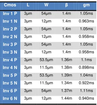
Table 6.1- W/L values of the transconductance block ...46
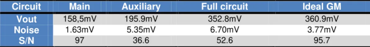
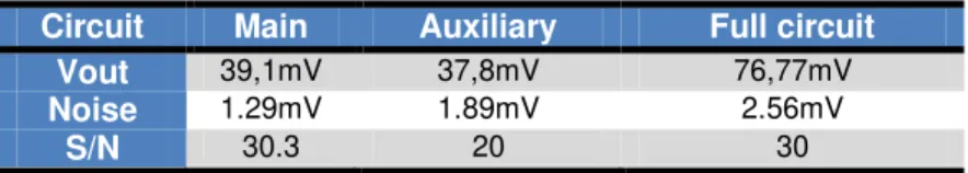
Table 6.2- Noise when using 100kΩ/100fF ...49
Table 6.3- Signal to Noise Comparison with an APD ...50
Table 6.4- Noise when using an APD and 83kΩ/100fF ...51
Table 6.5- signal to noise ratios for with an APD ...52
Table 6.6- feedback noise values when using 20kΩ/50fF with a SIPM ...55
Table 6.7- Signal to Noise Comparison using a SIPM and 20kΩ/50fF ...56
Table 6.8- Noise for 38kΩ/50fF with a SIPM ...57
Table 6.9- Signal to noise ratio for 38kΩ/50fF ...57
Table 6.10- APD 20kΩ/50fF ...59
Table 6.11- APD 20kΩ/50fF ...60
Abbreviations
APD
ADC
CS
CG
LNA
NF
NMOS
OA
PMOS
RCG
SIPM
TIA
VCVS
Avalanche Photodiode
Analog-to-Digital Converter
Common Source
Common Gate
Low Noise Amplifier
Noise Figure
Nchannel Metal-Oxide-Semiconductor
Operational Amplifier
Pchannel Metal-Oxide-Semiconductor
Regulated Common Gate
Silicone Photomultiplier
Transimpedance Amplifier
Chapter 1
Chapter 1 Introduction
1.1 Motivation
Radiation detectors are used in medical imaging, nuclear science and optical fields. In this work the focus will be the use of radiation detectors in medical applications, for the detection of breast cancer, using positron emission tomography (PET).
Breast cancer is one of the leading causes of dead among women; one in eight women will develop breast cancer during their lives [1]. Earlier detection of breast cancer improves the chances of it being treatable, thus reducing the mortality rate [3].
The current standard method of detection for breast cancer is the x-ray mammography, this technique has some limitations, like the fact that in women with high breast density it becomes difficult to detect the presence of tumors [2] other limitation is the fact that a mammography is unable to distinguish between a benign or malign tumor, this leads to a excessive number of biopsies being done, the PET is a response to the limitations of the mammography [3].
The PET scanner main function is the detection of cancer cells, this is achieved by taking into account a biological particularity of the cancer cells, their metabolism is higher than that of a normal cell. This means cancer cells will need a bigger quantity of glucose to support their higher metabolism.
To detect these cells a patient is injected with -fluoro-deoxy-glucose (FDG) which is a glucose with radiation markers, this glucose is absorbed in greater quantity by the cancer cells, due to their higher metabolism, making their detection possible [3].
The radiation produced by the FDG is detected by the scintillating crystal at the front end of a radiation detector, this crystal transforms incident radiation in to a light pulse, this pulse is then detected by a light sensitive device such as an avalanche photodiode (APD) or a silicon photon multiplier (SIPM).
The light sensitive device converts the light pulse, produced by the scintillating crystal into a current pulse, this current pulse is then transformed into a voltage pulse by a transimpedance amplifier (TIA) with a desired amplitude and shape to be used by an analog to digital converter (ADC).
Figure. 1.1 - Radiation Detector
The most commonly used light detectors are the Avalanche Photodiodes (APD), recently a new type of photo detector emerged, the Silicon Photomultiplier(SIPM), this detector has several advantages over the APD, like, a much higher gain, and a lower biasing voltage [4], this advantages come with a cost, The SIPM have much higher capacitance than the APD, this makes the use of the existing TIAs with the SIPM problematic.
The amplitudes and peaking time of the voltage pulse, are limiting factors to the performance of the detector. If the amplitude of signal produced by the TIA is too low, or the peaking time too high, the detector is going to have a lower resolution. A lower resolution leads to an increase in the radiation dose needed to be administer, or a increase in the examination time, both of this option exposes the patient to a higher dose of radiation[5].
Due to what was described the transimpedance block is a limiting factor on radiation detectors.
1.2 Objectives
The objective of this thesis is design and test of a TIA circuit that is used to transform a current pulse generated by an APD and a SIPM in to a voltage pulse with a suitable amplitude and shape Fig. 1.2 producing the less amount of noise possible.
t
100 ns
0
t
mv
o(
t
)
V
omt
I
dmi
d(t)
t
dFigure. 1.2- TIA with input current pulse id and output pulse v0
From Fig. 1.2 we have the magnitude of the current pulse and the time constant,
In this work two light detectors are used in conjunction with the proposed TIA, the more widely used APD (Avalanche Photomultiplier) and the more recent SIPM (Silicon Photomultiplier). This is done to compare the signal to noise ratio we are able to achieve with the two detectors in conjunction with the proposed circuit.
The APD was assumed to have an input capacity , and current pulse amplitude of . The SIPM is considered to have an input capacity and a current pulse amplitude of .
The output voltage pulse should be above 300mV, the necessary voltage amplitude for the ADC, and the peaking time 40ns, this must be achieved with the lowest amount of power consumption possible while having low noise.
(1.1a) (1.1b)
1.3 Thesis Organization
This thesis is divided in seven chapters, and, one appendix where noise equations for second order systems are deduced.
The first chapter starts with a small exposition of radiation detectors and the fields in which they are used, followed by the objectives and structure of this work, ending with a summary of the achieved results.
Chapter 2 consists of a brief overview of the function principles of photomultipliers, more specifically the APD (Avalanche Photomultiplier) and SPIM (Silicon Photomultiplier),
Chapter 3 is dedicated to the study of thermal noise in resistor and MOS transistors as well as flicker noise and noise cancelation.
On Chapter 4 two single stage amplifiers are study more specifically the Common-Source amplifier and the Common-Gate amplifier.
On Chapter 5 three existing TIA circuits are shown and, the feedback TIA, and the RCG TIA, for each one the transfer and noise function are deducted.
Chapter 6 is dedicated to the study of the proposed noise canceling circuit and its components, and the comparison between the use of and APD or a SIMP as the input photomultiplier.
Chapter 7 is where the make the final conclusions of the work done as well as plans for the future work that can be done in conjugation with was learned during this project.
1.4 Contributions
CHAPTER 2
Chapter 2 Photon detection
2.1 Basics
The considered photo detectors have as the base a p-n junction photodiode, where an incident photon with sufficient energy generates a current pulse; this current is then used to measure the light passing through.
When a p-n junction photodiode is reversed biased, an electric field is created; this field causes the holes in the p-type and the electrons in the n-type material to move away from the junction, causing a widening in the depletion region Fig. 2.1.
When a photon of sufficient energy interacts with the field an electron-hole pair is created. The field created by the reverse bias forces the electron and the hole from the par to drift respectably to the n and p sides Fig. 2.1, this movement of the electrons and holes generates a flow of photocurrent in the external circuit [6].
Depletion Region
n p
Photon
V
Figure. 2.1 - p-n photodiode
2.2.1-Avalanche Photodiodes (APD)
An APD is a p-n junction where the electric field is strong enough that a single charge carrier injected into the depletion layer, generates an electron-hole pair, that if created in the region of the strong electric field, has enough energy to generate another electron-hole pair by accelerating the electron or the hole with enough energy to impact in to the crystal lattice and through a process known as impact ionization generate another pair, thus generating an avalanche of secondary pairs [7].
This avalanche effect as two behaviors, one when the biased voltage is lower that the breakdown voltage, APD working in linear mode, and another then the biased voltage is higher that the breakdown voltage, the APD is working in Geiger mode.[7]
2.2.1.1- Linear Mode
If the biased voltage is lower that the breakdown voltage, the creation of new pair eventually starts to decline, because the rate at which new pair are created is lower than the rate at which they exit the high energy field region and are collected. This means that the number of pairs created by a single photon is limited to a fixed amount, for that reason the photocurrent generated is proportional to the incident flux of photons. In this mode of operation the internal gain is limited to M where M is the number of electron-hole pairs created on average by each absorbed photon and its value is in the order of tens or hundreds [7].
2.2.1.2- Geiger mode
In Geiger mode the biased voltage, is higher than breakdown voltage, this means that the electric field is so high that the avalanche created by a single charged carrier is self-sustaining. The rate at which new electro-hole pairs are created is higher than the rate a witch they are collected.
This self-sustaining avalanche causes a swift rise in the current .to the milliamp range in mere nanoseconds [8], Fig. 2.2 where the leading edge of the avalanche pulse marks the arrival time of the detected photon.
t
I
dmi
d
(t)
t
dThe current in a Geiger mode APD continues to flow until the avalanche is quenched by lowering the bias voltage to the same or below value of the breakdown voltage, this can be achieved using a resistance in series with the APD. As the current grows the voltage drop on the resistance causes the quenching of the APD. This effect reduces the voltage dropped across the high-field region, therefore slowing down the rate of growth of the avalanche, until a steady-state condition is reached where the bias voltage is decreased to the breakdown voltage, stopping the avalanche.
In Geiger-mode there is a chance that the avalanche stops early and photons go undetected, The number of electron-holes pairs created is typically higher that , much higher than in linear mode [7].
One problem with this type of APD is that they cannot be used to detected light. Intensity, the electrical pulse produced by the detection of one or more photons is indistinguishable; they can only be used to detect the presence of a light signal [8].
In this work a simplified model for the APD is used Fig. 2.3, this circuit is used to simulate the current pulse similar to the one in Fig. 2.2
i
dC
dFigure. 2.3- APD simplified model
Where a current source is in parallel with a capacitor this basic circuit simulates the effects of an APD when the values of and are properly set. The values used where 2,5μA for the current source and 10pF for the capacitor.
2.2.2-Silicon Photomultipliers (SIPM)
SIPM are a recent and promising class of light sensors that are comprised of a series of self-quenching, Geiger-mode APD connected in parallel Fig. 2.3. [4],[9]
Bias
V
The parallel connection unlike the Geiger Mode APD allows the SIPM to carry information on light intensity. What makes this detectors so promising is its high quantum efficiency, the probability of a photon being absorbed in the active region of the device, the much higher gain when comparing with the linear APD, low bias voltage, insensitivity to magnetic fields, a good time resolution and a small size [9].
CHAPTER 3
Chapter 3 Noise
Electronic noise is a random fluctuation in an electrical signal, these fluctuations are present in all electronic circuits, noise can be caused by physical phenomena due to the nature of the materials in use, or by external interferences.
Noise is random in nature, for that reason its instantaneous amplitude cannot be determined making its study somewhat difficult, while we cannot determine the noise amplitude, by observing noise signals for some time and using this data to create statistical models we are able to determine its average power [11],[12]
The presence of noise in electronic circuits is inevitable, for that reason it is important to analyze its impact on the degradation of the desired signals so that its effects can be minimized.
In this chapter the main noise sources in CMOS transistors are presented.
3.1 Thermal noise
Thermal noise, also called Jonhsom noise or Nyquist noise is the result of random thermal motion of charge carriers inside an electrical channel; this motion introduces a variation in the voltage measured across the conductor even when the average current is zero. The thermal noise power is proportional to the absolute temperature and can be quantified by,
(3.1)
where k is the Boltzmann constant, T the temperature in Kelvin and the bandwidth of the system, to simplify it is assumed that .
n2
v
i
n 2Figure. 3.1- Thermal noise resistor model
Where and are, respectively,
(3.2) (3.3)
with the Boltzmann constant, and T is assumed to be 300K.
Thermal noise in MOS transistors is also present due to carrier motion through the channel, thermal noise is the main source of noise in transistor, and can be modeled as a voltage source connected to the gate or a current source connected between the drain and source
2
v
i
n 2 nFigure. 3.2- MOSFET thermal noise model
If the transistors are operating in triode we have [13]
(3.4) (3.5)
(3.6) (3.7)
where is the transistor transconductance and γ is assumed to be 2/3 for long-channel transistors and higher for small submicron transistors.
3.2 Flicker Noise
Flicker noise in MOS transistors is caused by a physical phenomenon, this noise is believed to be caused by the imperfections on the interface between the gate oxide ( ) and the silicon substrate ( ), this imperfections lead to charge carriers being randomly trapped and released causing the appearance of noise in the drain current.
This phenomenon is more prevalent at low frequencies, for this reason flicker noise is also called 1/f noise. Flicker noise is modeled as a voltage source in series with the gate and is given by [11]
(3.8)
From (3.8) we have K that is a bias independent constant that varies with the technology in use, Is the gate oxide capacitance, W and L the width and length of the transistor. One way to reduce flicker noise is the use of a cleaner fabrication process; this reduces the value of K, thus reducing flicker noise. The exponent c varies between 0.7 and 1.2 but is usually closer to 1.
Flicker noise in p-channel devices is generally smaller than in n-channel devices of the same dimensions and fabricated with the same CMOS process, this is believed to be caused by the fact that in p-channel devices, the channel is farther away from the interface, this decreases the likelihood of a charged carry being randomly trapped and released [12].
Flicker noise is still being actively studied, to better understand its origins, and how to better predict its appearance.
3.3 Noise Cancellation
RF receivers require LNAs with a sufficient large gain, a noise figure (NF) below 3 db, good linearity and a matching resistor that ensures impedance matching ,
VIN V o Current Measurement Path Voltage Measurement Path Rs RIN
IRIN
VRIN αVRIN
IRIN rm
t
t
noise noise noise v2 Rs v2 RINFigure. 3.3- Noise cancelling theory using.
The output signal of the NC-LNA of Fig. 3.3 is the difference between the voltage measurement path and the current measurement path . knowing that the gain is
(3.9)
and the noise factor
(3.10)
If we set the relative gain of both the voltage measuring and current measuring paths so that we have
(3.11)
the input signal appears differential at the output while the matching resistor noise appears as common-mode. In Fig. 3.4 we can see the relation between the noise figure and the relative gain of the paths, when the noise figure equals zero.
N
F
[d
B
]
Path Gain [rm/α]
NF=0
Figure. 3.4- Noise figure in relation with path gain.
CHAPTER 4
Chapter 4 Single stage MOS Amplifiers
4.1 Common Source Stage
The common-source amplifier Fig. 4.1 is a basic single-stage amplifier that converts variations in its gate-source voltage to a small drain current, this current flows through a resistor load to generate an output voltage, this stage as a high input and output impedance and voltage gain[11],[16].
V
oV
DDR
XM
1V
inFigure. 4.1- Common Source amplifier with resistive Load
Since the bulk and source of the transistor are connected to the same voltage potential the body effect can be ignored during the study of the common-source.
4.1.1 Low frequency model neglecting
g
m1V
gs1V
gsR
DV
inV
outFigure. 4.2- Small-signal model of the Common-Source amplifier without r0
From the small-signal model we have
(4.1)
From (4.1) the gain can be written as
(4.2)
4.1.2 Low frequency model with
Now the small-signal model of the Common-Source amplifier taking into account Fig. 4.3 is analyzed
g
m1V
gs1V
gsR
DV
inV
outr
0Figure. 4.3- Small-signal model of the common-source stage with
From the circuit on Fig. 4.3 we can see that is in parallel with so by using (4.2) and replacing with the equivalent parallel resistance we obtain
(4.3)
Replacing we obtain
4.2 Common Gate Stage
A Common-Gate amplifier produces an output at the drain by sensing the input signal at the source as can be seen in Fig. 4.4 [11],[16]. In addition to the gain the input impedance is also obtain for this amplifier.
V
oV
DDR
M
1V
V
inB
R
S DFigure. 4.4- Common Gate With Resistive Load
As was the case with the common-source amplifier we start by analyzing the simpler small-signal model of the common-gate without taking into account, from the circuit, we the equations of the gain and impedance. We then repeat the process for the circuit with .
In the common-gate amplifier since the source is connected to a variable voltage source, and the bulk to a constant voltage source we have to take into account the body effect [16], the body effect is represented in the small signal model by an voltage controlled current source which depends on source-bulk voltage.
4.2.1 Low frequency model neglecting
4.2.1.1 Gain
g
m1V
gs1V
gsR
DV
g
mV
V
inR
S
out
sb
From Fig. 4.5 the current passing through can be written as
(4.5)
And
(4.6)
Since
(4.7)
If we replace (4.5) and (4.7) in (4.6) we obtain
(4.8)
4.2.1.2 Input Impedance
In Fig. 4.6 it´s shown that the input impedance is viewed from the source of transistor
g
m1V
gs1V
gsR
DV
g
mV
out
sb
i
i
Z
inFigure. 4.6- Small signal model input impedance without r0
From Fig. 4.6 we can see that , for this reason (4.6) can be written as
(4.9)
from (4.9) we can write as
4.2.2 Low frequency model with
4.2.2.1 Gain
The small-signal model of the Common-Source amplifier taking into account can be seen in Fig. 4.7
g
m1V
gs1V
gsr
0R
DV
outg
mV
sbV
inR
S
Figure. 4.7- Small signal of the common-gate amplifier with r0
From the circuit we can see that the current flowing through is equal to the current flowing through , so we have
(4.11)
With we can write as
(4.12)
Since the current through is equal to
(4.13)
From the circuit can be expressed as
(4.14)
Replacing (4.12) and (4.13) in (4.14) we have
4.2.2.2 Input Impedance
To obtain the impedance at the source taking into account we analyze the circuit of Fig. 4.8
g
m1V
gs1V
gsr
0R
DV
outg
mV
sbZ
ini
i
Figure. 4.8- Small signal model input impedance with r0
From the circuit in Fig. 4.8 we have that and since
(4.16)
with
(4.17)
we have
CHAPTER 5
Chapter 5 Transimpedance Amplifiers
In this chapter we are going to describe three existing types of transimpedance amplifiers used to transform the current signal produced by the APD or the SIPM into a voltage pulse with a suitable amplitude and shape. The circuits described n this chapter are; the feedback TIA, the Common Gate TIA and the Regulated Common Gate TIA.
5.1 Feedback TIA
The feedback TIA will be shown in a little more detail than the CG TIA and RCG TIA since this is the base of the proposed circuit.
The feedback TIA consists of an operational amplifier (OA) with a first order RC feedback loop as can be seen in Fig. 5.1.
C
f
R
f
I
d
C
d
V
o
-
A
(
s
)
5.1.1 Transimpedance function
If we assume that the OA present in the feedback is ideal, the transimpedance function is simply the feedback impedance [17],
(5.1)
(5.2)
Since the first pole of the OA can be located close to the other poles of the circuit we cannot assume that the AO is ideal [18], for that reason the AO is assumed to have a dominant pole. With a dominant pole the gain of the circuit can be written as
(5.3)
where is the low-frequency gain of the OA and is assume to be much larger than one, . We also know that the gain-bandwidth product of the OA is
(5.4)
From the circuit we have
(5.5)
where
(5.6)
and assuming that
(5.7a) (5.7b) (5.7c) we obtain [18],
We have a two pole transimpedance function that can be written as
(5.9)
Comparing (5.9) with (5.8) we obtain
(5.10a) (5.10b)
Since and must be of the same order it is assumed that they are real an equal, with the same time constant. Since the proposed circuit is going to be tested with both an APD and a SIPM we are going to compare the two of them when using a feedback TIA.
When using an APD we have a low input capacitance and a small current pulse . Making and the minimum value needed to achieve the required peaking time, replacing the this values in (5.10a) and (5.10b), we easily obtain with and a , both are acceptable values.
With the SIPM we have a much higher value of and a smaller feedback resistance, , replacing this values in (5.10b) for , we have
, this value of B is too small for the technology in use today, this means that then using a SIPM in conjunction with a feedback TIA, the time constant is going to be high.
. To allow for a higher value of B can be lowered while maintaining the same pulse shape by using a second stage Voltage Controlled Voltage Source (VCVS) Fig. 5.2, with a voltage gain h. This second stage must be wide band enough to assure that the pulse shaping performed by the first stage TIA is not significantly affected.
C
fR
fId
C
d-
A
(
s
)
V
oh
VCVS
Figure. 5.2- Feedback with a VCVS
With the second stage VCVS (5.9) can be written as
(5.11)
(5.12)
This method allows us to have a higher output voltage pulse while maintaining the same .
5.1.2 Noise Analysis
The feedback TIA as two noise sources the OA and the resistor of the parallel RC circuit, the noise of the OA can be simulated as a voltage source at the input and the noise generated by the resistor can be simulated by a current source in parallel with , both noise sources can be seen in Fig. 5.3, Since we are going to use wideband TIAs flicker (or 1/f) noise is not considered.
R
fI
dC
dV
o
-
A
(
s
)
C
fnf
na
V
I
Figure. 5.3- Feedback TIA noise sources
5.1.2.1 Noise contribution of OA
The input transistor is assumed to be the dominant noise source of the OA, the spectral density of the input noise voltage of the OA is
(5.13)
Where is the transconductance of the input transistor of the OA. First we are going to calculate the noise contribution of OA, for that reason we are going to ignore the current source
Fig. 5.3 while calculating the noise function N(s).
Assuming that
(5.15a) (5.15b) (5.15c) We have
(5.16)
N(s) has one zero and two poles and can be express as
(5.17)
Where
(5.18a) (5.18b) (5.18c)
To obtain the rms output noise voltage equation (A.5) from the Appendix is used
(5.19)
From (5.18a) and (5.18c) we can write
(5.20)
Replacing (5.18b) and (5.20) in (5.19 ) and assuming we obtain
(5.21)
When using an APD, assuming that , , and
For the SIPM with that , , and we obtain
5.1.2.2 Noise contribution of
The noise generated by the resistor can be simulated by an current source in parallel with the resistor as can be seen in Fig. 5.3, where
(5.22)
The current source that simulates the noise produced by the resistor can be replace with two current sources Fig. 5.4. The current source that is connected to the output of the amplifier can be neglected since it is connected to a low impedance node [18], this means that we only have to consider the current source at the input, since this current source is in the same place as the noise function can be written as
(5.23)
C
fR
fI
dC
dV
o
-A(s)
nf
I
nf
I
Figure. 5.4- Feedback TIA resistor noise
From the Appendix using equation (A.7) we have
(5.24)
(5.25)
When using an APD, assuming that , , and we obtain
For the SIPM with that , , and we obtain
The noise contribution of the resistors is very small in comparison to the noise of the OA, if we compare the two noise contribution we have
(5.26)
Replacing (5.20) on (5.26), assuming the use of an APD as the input with we get
(5.27)
5.2 Common Gate TIA
The Common-Gate TIA Fig. 5.5 is another type of TIA that can be used to transform the current pulse of a light sensitive device into a voltage pulse.
V
oV
DDR
XM
1C
dI
dC
XI
B1V
BFigure. 5.5- Common Gate TIA
5.2.1 Transimpedance Function
Neglecting thebody effect, the input impedance of the common-gate isapproximately
(5.28)
from the circuit the current at the source of the transistor is [18]
(5.29)
this current is the same as the one at the load impedance , this means that,
(5.30)
with
(5.31)
(5.32)
From (5.32) we have two poles,
(5.33a) (5.33b) To keep the value of low so as to keep the DC voltage drop in low, a voltage post-amplifier can be connected to the output of the common-gate TIA as can be seen in Fig. 5.6, this amplifier would function in the same way as the one at the feedback TIA, by amplifying the output by a factor of h we can replace for .
V
oV
DDR
XM
1C
dI
dC
XI
B1V
Bh
VCVS
Figure. 5.6- Common-Gate with a voltage post-amplifier
With the post-amplifier the transfer is now
(5.34)
With a APD at the input we have and if we make we obtain and we can use , with
Replacing the input APD by a SIPM means that now and , for
5.2.2 Noise Analysis
The Common-Gate TIA as three noise sources, the first one is the noise generated by the bias current source, the second one is the thermal noise generated by the M1 transistor, and finally represents the noise of the resistor [19]. This three noise sources are shown in Fig. 5.7.
V
oV
DDR
XM
1C
dI
dC
XI
B1I
nBI
n1I
nxFigure. 5.7- Common Gate TIA noise sources
Where the respective spectral densities of each noise source are
(5.35a) (5.35b) (5.35c)
Assuming that the MOS transistors noise coefficient is γ=1, and assuming that the bias current source is replaced by a transistor with a constant value of and transconductance, we have from [19] that for
5.2.2.1 Noise contribution of
In the case of we have
(5.36)
(5.37)
The noise generated by cannot be minimized because it consists only of variables used to determine the circuit time constants.
5.2.2.2 Noise contribution of
In the case of since it is in the same position as we can use equation (5.32)
(5.38)
in this case we have a two pole, using equation (A.7) and (5.35c) we have
(5.39)
where and are respectably (5.33a) and (5.33b). In this case the noise can be reduced by using a small value of , since this is the only variable on (5.39) that we can change without affecting the circuit time constant.
5.2.2.3 Noise contribution of
To calculate the noise contribution of the incremental circuit of Fig. 5.8 is used, there we have the incremental resistance of the bias current source and the transistor model resistance .
C
XR
XR
r
C
do1
oB
V
gsV
nog
m1V
gsI
n1Figure. 5.8- Small signal model of the CG with noise source
Taking into account that and and assuming that we have [19]
Using equation (A.5) and knowing that and we have
(5.41)
From (5.28) the only way to minimize the noise contribution of is by increasing the value of
5.3 Regulated Common Gate
The regulated Common-Gate TIA was developed as a response to the shortcomings of the common-gate TIA. The RCG TIA can be described as a common-gate stage (transistor , with bias current and load resistor ), with a voltage amplifier with gain A (common-source transistor with active load ) Fig. 5.3 [19].
Vo
VDD
IB2
RX
M1
M2
IB1 Cd Id
(RoB2 )
(RoB1 )
CX
Vo
VDD
RX
M1
Cd
Id
CX
IB1 -A
(a) (b)
Figure. 5.9- Regulated Common Gate
In Fig. 5.9a we can see the RCG circuit and in Fig. 5.9b a simplified version where the feedback loop created by the extra voltage gain stage can be easily seen.
5.3.1 Transimpedance Function
We can see on Fig. 5.3b that the common-source transistor with active load is an amplifier stage with voltage gain A [19]
(5.42)
Where is the incremental resistance of the load . The input impedance can be written as
(5.43)
(5.44a) (5.44b) (5.44c) (5.43) Can be simplified to
(5.45)
From Fig. 5.9 since the input current is divided between and the input impedance we have for the incremental source current of [18]
(5.46)
This current flows through
(5.47)
So from (5.46) and (5.47) we have
(5.48a) (5.48b)
The transimpedance function is then [18]
(5.49)
The advantage of this circuit when comparing with the CG is that now doesn’t rely exclusively on , this means that for a maximum value of we can have a much smaller while maintaining the same time constant.
With a SIPM at the input and , and for we now have which is an acceptable value.
5.3.2 Noise Analysis
V
oV
DDI
B2R
XM
1M
2I
B1C
dC
XI
I
I
I
n1 n2 nB1 nB2Figure. 5.10- RCG TIA incremental circuit with noise sources.
The spectral densities of the noise sources are
(5.50a) (5.50b) (5.50c) (5.50d)
The equivalent noise circuit with the noise sources can be seen in Fig. 5.11.
RoB
ro1
gm1Vgs1
Cd
Vi InB1
Vgs1
gm2Vi
In1
InB2
In2
Z =X R //X C X
Vno
ro2 2 RoB1
5.3.2.1 Noise contribution of
For the noise [18] assuming that
(5.51a) (5.51b) (5.51c)
We have
(5.51)
Where
(5.52)
With and from (5.48a) and (5.48b)
Using (A.5) on (5.51) to obtain the rms output noise voltage due to the common gate transistor noise we have
(5.53)
Replacing (5.50a) and (5.52) on (5.54) and considering that we obtain
(5.54)
5.3.2.2 Noise contribution of
For the noise source we have [18]
(5.55)
With , and from (5.52) (5.48a) and (5.48b), respectively Using equation (A.5) the rms noise voltage due to is
(5.56)
(5.57)
The noise contribution of can be decreased, by increasing the value of
5.3.2.1 Noise contribution of
For the noise source since it is in the same place as we use (5.49). Using equation (A.7) on (5.49) we obtain
(5.58)
Replacing (5.50c) on (5.58) we obtain
(5.59)
5.3.2.1 Noise contribution of
For the noise since it is in the same place as we use (5.55). Using equation (A.5) on (5.55) we obtain,
(5.60)
Replacing (5.52) and (5.50d) on (5.60) and considering that we obtain
(5.61)
CHAPTER 6
Chapter 6 Proposed Circuit
In this chapter the proposed circuit is presented and studied, we start with a brief introduction to the circuit, then we deduce the transfer and noise function of the circuit, this is followed by the simulations results, where the circuit is tested with an APD and a SIPM at the input, the results are then compared with the known feedback circuit.
Finally the APD and the SIPM are compared with each other when in use with the same feedback values.
6.1 Feedback TIA with Auxiliary Path
The circuit in study consists of two feedback TIAs connected at the input with one of then having a extra transconductance block. The objective of this work is to, try and reduce the noise produced by the TIA, when used in conjunction with a photo-detector, by adapting a noise canceling circuit used in RF circuits,
This circuit has two path, the main path where we have a simple feedback TIA and an auxiliary path where a Gm block inverts the input voltage signal produced by the APD or SIPM into a current signal, this signal is then converted back to a voltage signal by a second feedback TIA complementary to the one presented on the main path, this results in a signal with the same amplitude but 180º out of phase [15]. During this work we will refer to the feedback TIA without the transconductance block as the main path and the TIA with the transconductance block at the input as the auxiliary path
C
fR
fI
dC
dV
o-
A
(
s
)
C
fR
f-
A
(
s
)
G
mt
t
Main Path
Auxiliary Path
Figure. 6.1- Proposed circuit.
The transconductance block GM in Fig. 6.1 is in its simplest form a Class-AB CMOS inverter, as can be seen in Fig. 6.2, this block is used to invert the phase of the input signal by 180º without adding gain. In this circuit the voltage measurement is provided by the auxiliary path and the current measurement by the main path.[15]
M
1M
2in
out
V
I
C
LoadFigure. 6.2- Class-AB CMOS inverter
From Fig. 6.2 can be written as
(6.1)
Inv 2
Inv 3 Inv 4 Inv 5 Inv 6
Inv 1
Vdd
Vdd
Vdd Vdd Vdd Vdd
Cint
I V
o2
Io1
o1
Vo2
Gm
Figure. 6.3- Complete Transconductance element of the auxiliary path
The circuit shown in Fig. 6.3 as no internal nodes and has a good linearity in V-I conversion if the β factors of the n-channel and p-channel transistors are perfectly matched. [20] The output differential current of the circuit Fig. 6.3 is
(6.1)
Where
For differential output signals and are virtually loaded with
(6.2a) (6.2b)
And for common mode output signals
(6.3a) (6.3b)
The dc gain of the transconductor can be increased by loading the differential inverters Inv1 and Inv2 with a negative resistance, this can be achieved by making
, simply by making the width of Inv 4,5 slightly smaller than that of Inv 3,6. This negative
resistance can be implemented without adding extra nodes to the circuit, this can be used to adjust the gain of GM to ensure that the input and output signals are as equal as possible. [20]
6.2 transfer function
We have for the main and auxiliary path the same transfer function as the one from the feedback TIA studied in chapter 3 but with opposite signs, assuming that the transconductance block inverts the phase by 180º without adding gain or adding internal nodes.
For the main path we have as was seen in chapter 5
(6.2)
By comparison the transfer function of the auxiliary path is going to be equal but with a different sign
(6.3)
Combining the paths we obtain
(6.4)
This means that when using this circuit we have double the voltage gain while using the same values as where used in the feedback TIA.
6.3 Noise Function
From [18] we know that the noise effect of the transconductance block on the main path is
Inv 1 Vdd
2
vn
Figure. 6.4- Inverter noise contribution to the main path
Where
(6.5)
From [19] we now that the differential output noise of the transconductor of Fig. 6.3 is
(6.6)
Where is the total sum of all the transconductances of the six inverters present on the GM block, this will later be proven problematic when dealing with an APD an its low current pulse amplitude. The total noise sources of the full circuit can be seen in Fig. 6.5.
Id Cd
Vo
Gm
Cf
Rf
-A(s) Inf
na
Vngm Ingm
Cf
Rf
-A(s) Inf
na
Main Path
Auxiliary Path
6.3.1 Main path noise
In the main path we have as noise sources the GM block, the OA noise and the feedback resistor, as was shown in chapter 5 the feedback resistor can be ignored, since in the feedback TIA the noise caused by the OA is dominant, this leaves us with only the need to calculate the noise contribution of the OA and the GM
6.3.1.1 Noise contribution of GM
We start by calculating the noise impact of on the main path, for that reason the other noise sources are going to be ignored for now; since is in the same place as we can use equation (5.18a) replacing for we have
(6.7)
From equation (A.5) from the appendix we have
(6.8)
From (5.17) and (6.5 )with we obtain
(6.9)
Assuming that we have
For the APD with , ,
And for the SIPM with , ,
6.3.1.2 Noise contribution of OA
Now we only need to calculate the noise contribution of the OA from (5.21) we have with
(6.10)
Assuming that we have
With a SIPM with , ,
6.3.2 Auxiliary path noise
In the auxiliary path we have to calculate the noise contribution of the OA and the GM, the resistor noise as was said before can be ignored.
6.3.2.1 Noise contribution of GM
We start by calculating the noise contribution of GM, since the current source that simulates the noise contribution of GM is in the same place as as can be seen in Fig. 6.6, we can use equation (5.23)
C
fR
fV
o-
A
(
s
)
ngm
I
Figure. 6.6- Feedback TIA with GM noise
From the Appendix (A.7) we have for (5.23)
(6.11)
Replacing (6.6) in (6.11) we have
(6.12)
The value of is highly dependent on the feedback resistor, this means that when using an APD at the input can be very high due to the high values of needed to compensate the low input signal generated by the APD. Assuming that we have;
For the APD with , and
For the SIPM with , and
As was expected we have a much higher value of when using an APD at the input, further on this relation between the noise generated by GM on the auxiliary path and the feedback resistor will be shown during the simulation.
6.3.2.2 Noise contribution of OA
Now that we have the noise generated by GM we only need to calculate the noise contribution of the OA from (5.21) we have with
(6.13)
In the case of the APD with , and assuming that
In the case of the SIPM with , and assuming that
6.4 Simulation result
6.4.1 Simulation Setup
The circuit in test was design using Cadence Virtuoso Analog Design Environment version 5.1.41,using 130μm transistor model Bsim version 3.3 with a 1.2V Vdd and simulated using Spectre Circuit Simulator version 7.11.
6.4.1.1 OA Block
The Operational amplifier in use is a Folded-Cascode Operational-transconductance amplifier (OTA) Fig. 6.7, with an open loop gain of 62dB. This amplifier was design and optimized as a project from design of analog circuits and Systems class, under the supervision of professor João Goes using Mathcad as can be seen in appendix B1.
V
DDV
NM7
NM6
NM8
NM11
NM9
NM10
NM12
PM7
PM6
PM5
PM4
V
V
V
B1
B4 B2
V
ipB3
V
in
V
out
Figure. 6.7- Simplified Folded Cascode without polarizing circuit
When a feedback is applied to this amplifier, the gain decreases to 45.4 dB, when using a feedback with 100kΩ and 100fF, as is the case when an APD is in use, and to 31.4dB for a feedback of 20kΩ and 50fF, in the case of the SIPM.