Afonso da Cunha Ferreira
Licenciado em Ciências de Engenharia de Micro e Nanotecnologias
Perylene Diimide acceptors: Fabrication
and characterization of electron-only,
hole-only devices and solar cells
Dissertação para a obtenção do Grau de Mestre em
Engenharias de Micro e Nanotecnologias
Orientador: Paul Blom, Professor Doutor, Max Planck Institute for Polymer Research
Co-orientador: Isabel Ferreira, Professora Doutora,
Faculdade de Ciências e Tecnologia da Universidade Nova de Lisvoa
Júri:
Presidente: Prof. Doutor Rodrigo Ferrão de Paiva Martins
Arguente: Prof. Doutor Luiz Fernando Ribeiro Pereira
Vogal: Prof. Doutora Isabel Maria Mercês Ferreira
Perylene Diimide acceptors: Fabrication and characterization of electron-only, hole-only devices and solar cells
Copyright ©Afonso da Cunha Ferreira, Faculdade de Ciências e Tecnologia, Universidade Nova de Lis-boa.
Acknowledgments
I would like to start off by sending a sincere thank you to everyone who helped me throughout my academic years and in my dissertation. It has been a challenging but rewarding time in my life. I realize that it will not be possible to mention every single person from these 5 years and I apologize to those who I forgot to include in these acknowledgments, however I will try to make justice to everyone.
First of all, I would like to thank Dr. Paul Blom and Dr. Irina Crăciun for giving me the opportunity to work alongside such an amazing team at Max Planck Institute for Polymer Re-search (MPIP), in an institute and reRe-search group with great recognition in the field, and for an experience that will not be forgotten. Thank you for your support and knowledge input during my time there.
Also a special thanks to Selen for all your help and mentoring. Thank you for all your pa-tience while introducing me to a research topic I was not too much familiar with and for guiding me almost every day and teaching me the ropes of conducting proper scientific research.
Thank you so much to my co-advisor, professor Dr. Isabel Ferreira, that besides the distance was always ready to help in any problem that I encountered. Thanks for being such a good teacher, for all those long meetings helping me understand and analysing results and specially for the last minute rescues. The last few weeks were very stressful but the professor was very supportive and available. I thank you again.
A big thanks to all my friends from across the world that I met in Erasmus. You already know that you have a permanent couch here in Portugal and I hope to continue seeing you guys for years to come. A-town friends forever.
Thanks to my colleagues and friends who I have met at university and who have accompa-nied me from the start. A special mention to both the original and adopted members of the iconic house "Basolho", that became really close friends of mine and with whom I have shared wonderful moments. Çim.
Also I could not help but to send a huge, huge hug to all the "gang" from Queijas and out-skirts and life-long best friends. I don’t think I need to say who you are because you all already know. We are all stepping into a different phase in our lives that is full of uncertainty and where we may not see each other all the time, but I know for sure that this friendships will endure. É para a vida "mos putos".
Abstract
The thrust towards energy conservation and reduced environmental footprint has fueled inten-sive research for alternative low cost sources of renewable energy. Organic photovoltaic cells (OPVs), with their low fabrication costs, easy processing and flexibility, represent a possible viable alternative. Perylene diimides (PDIs) are promising electron-acceptor candidates for bulk heterojunction (BHJ) OPVs, as they combine higher absorption and stability with tun-able material properties, such as solubility and position of the lowest unoccupied molecular orbital (LUMO) level. A prerequisite for trap free electron transport is for the LUMO to be located at a level deeper than 3.7 eV since electron trapping in organic semiconductors is uni-versal and dominated by a trap level located at ∼3.6 eV. Although the mostly used fullerene
acceptors in polymer:fullerene solar cells feature trap-free electron transport, low optical ab-sorption of fullerene derivatives limits maximum attainable efficiency. In this thesis, we try to get a better understanding of the electronic properties of PDIs, with a focus on charge carrier transport characteristics and the effect of different processing conditions such as annealing tem-perature and top contact (cathode) material. We report on a commercially available PDI and three PDI derivatives as acceptor materials, and its blends with MEH-PPV (Poly[2-methoxy-5-(2-ethylhexyloxy)-1,4-phenylenevinylene]) and P3HT (Poly(3-hexylthiophene-2,5-diyl)) donor materials in single carrier devices (electron-only and hole-only) and in solar cells. Space-charge limited current measurements and modelling of temperature dependentJ-V characteristics con-firmed that the electron transport is essentially trap-free in such materials. Different blend ratios of P3HT:PDI-1 (1:1) and (1:3) show increase in the device performance with increasing PDI-1 ratio. Furthermore, thermal annealing of the devices have a significant effect in the solar cells that decreases open-circuit voltage (Voc) and fill factor FF, but increases short-circuit current
(Jsc) and overall device performance. Morphological studies show that over-aggregation in
Resumo
O recente impulso para a conservação de energia e redução da pegada ambiental tem vindo a alimentar intensa investigação ciêntifica por fontes alternativas de energia renovável e de baixo custo. Células fotovoltaicas orgânicas (OPVs), tendo custos de fabricação baixos, sendo de fácil processamento e permitindo dispositivos mecânicamente flexíveis, representam uma possível alternativa viável. Derivados de perileno diimida (PDIs) são candidatos promissores para a substituição de derivados de fulereno em células solares de heterojunção de volume (BHJ). Os PDIs combinam uma maior absorção e estabilidade com a possibilidade de ajustamento de certas propriedades do material, tais como a solubilidade e a posição da orbital molecular desocupada mais baixa (lowest unoccupied molecular orbital, LUMO). Um pré-requisito para o transporte de electrões livre de "armadilhas"energéticas é que o LUMO esteja abaixo de 3.7 eV, uma vez que o aprisionamento de electrões em semicondutores orgânicos é universal e dominado por um nível energético de armadilhamento localizado a ∼3.6 eV. Embora os fulerenos mais
usados como material aceitador de electrões em células solares de sistemas polímero:fulereno disporem de um transporte de electrões livres de armadilhamento, a baixa absorpção óptica dos derivados de fulereno impõe um limite máximo na eficiência obtenível. O objectivo deste trabalho consistirá em obter uma melhor compreensão das propriedades eletrónicas dos PDIs (com foco no transporte de portadores de carga) e o efeito de diferentes condições de processamento, tais como o tratamento térmico, material do contacto superior (cátodo), entre outras. Nós reportamos sobre um PDI disponível comercialmente e três derivados de PDI como materiais aceitadores de electrões e a sua combinação com os materiais dadores de electrões, MEH-PPV (Poli [2-metoxi-5- (2-etilhexil oxi) -1,4-fenilenovinileno]) e P3HT (poli (3-hexiltiofeno-2,[2-metoxi-5-di-il)), em dispositivos com um único portador de carga (electrões, eletron-only, e buracos, hole-only) e em células solares. Medições de correntes limitadas por cargas espaciais e modelagem de características J -V dependentes de temperatura, confirmam que o transporte de eletrões, em tais materiais, é livre de armadilhamento. Misturas de P3HT:PDI-1 com diferentes proporções de (1:1 e (1:3) mostram um melhoramento no desempenho do dispositivo com o aumento da proporção de PDI-1. Além disso, o tratamento térmico dos dispositivos tem um efeito significativo nas células solares, efeito esse que diminui a tensão em circuito aberto (Voc) e ofill factor (FF), mas que aumenta
a corrente de curto-circuito (Jsc) e o desempenho geral do dispositivo. Estudos morfológicos
Contents
1 Introduction 1
1.1 Conjugated polymers . . . 1
1.1.1 Carrier transport . . . 3
1.1.2 Electronic trapping in organic semiconductors . . . 4
1.2 Device characteristics of organic solar cells . . . 5
1.3 Perylene Diimides . . . 6
2 Materials and Methods 7 2.1 Substrate Cleaning . . . 7
2.2 Solution synthesis . . . 7
2.2.1 Solution Solvents . . . 7
2.2.2 Donor and acceptor materials . . . 7
2.2.3 Active Layer Solution (P3HT:PDI and P3HT:PCBM) . . . 7
2.3 Device fabrication . . . 7
2.3.1 Material deposition . . . 7
2.3.2 Contact evaporation . . . 8
2.3.3 Thermal Annealing . . . 8
2.4 Device characterization . . . 8
2.4.1 Atomic force microscopy (AFM) . . . 8
2.4.2 Electrical characterization . . . 8
2.4.3 Simulation . . . 8
3 Results and Discussion 9 3.1 P3HT:PCBM system . . . 9
3.2 Donor:PDI systems . . . 11
3.2.1 AFM characterization of PDI films . . . 11
3.2.2 MEH-PPV:PDI-1 . . . 13
3.2.3 P3HT:PDI-1 . . . 15
3.3 PDI derivatives . . . 23
4 Conclusions and future perspectives 30
List of Figures
1.1 Schematic representation of the electronic bonds between carbon atoms (above) and the chemical structure of polyacetylene, comprising of alternating single and double bonds between the carbon atoms (below). Adapted from . . . 2 1.2 Schematic layout of a typical bulk-heterojunction solar cell. A section of the
active layer is enlarged to illustrate the processes of light absorption and charge generation/collection. . . 2 1.3 Schematic energy-band diagram of a bulk-heterojunction organic solar cell. The
solid lines represent the energy levels of the donor, while the dashed lines represent the energy levels of the acceptor. Adapted from . . . 3 1.4 Schematic energy level diagrams in single carrier devices. Both are under forward
bias . . . 3 1.5 Schematic representation of bimolecular recombination and the four processes
involved in recombination by trapping: (a) bimolecular, Langevin recombination, (b) electron capture, (c) electron emission, (d) hole capture, and (e) hole emission. 4 1.6 Typical current density-voltage characteristic of an organic bulk-heterojunction
solar cell. The characterization parameters Jsc,Voc, and FF are indicated. The
maximum-power point (Mpp) is also shown, where the maximum powerPmaxthat
the solar cell can supply is represented by the filled rectangle. . . 5 1.7 Illustration of the chemical structure of the PDI base structure and the possible
positions for the tuning of its properties. . . 6
3.1 J-V characteristics of P3HT:PCBM (1:1 wt/wt) solar cells (a) under light and (b) in dark. (c)Voc vs light intensity of the same solar cells. . . 10
3.2 AFM pictures of pristine PDI-1 films annealed for 30 min at (a) 50°C, (b) 60°C and (c) 80°C. . . 12 3.3 AFM height images of P3HT:PDI-1 blend films with different PDI fraction, cast
from CB and CF, non-annealed and annealed. (a) As-spun P3HT:PDI-1 (1:1 wt/wt) film cast from CB; (b) As-spun P3HT:PDI-1 (1:1 wt/wt) film cast from CF; Annealed (10 minutes at 100°C) P3HT:PDI-1 (1:1 wt/wt) film cast from CF; and annealed (10 minutes at 100°C) P3HT:PDI-1 (1:4 wt/wt) film cast from CF. 13 3.4 J-V characteristics for the non-annealed (blue) and post annealed (red)
MEH-PPV:PDI-1 (1:4 wt/wt) devices (a) under light and (b) in dark. The inset of (b) shows the differential plot of the data according to equation 3.1. . . 14 3.5 (a) Experimental J-V characteristics (symbols) of a non-annealed (blue) and
annealed (red) MEH-PPV:PDI-1 (1:4 wt/wt) EO device and (b) again of a non-annealed device at reverse bias. The solid line is an automatic linear fit to the experimental data with slope 1. . . 15 3.6 Temperature-dependentJ-V characteristics of a non-annealed EO device with a
MEH-PPV:PDI-1 (1:4 wt/wt) active layer system. . . 15 3.7 (a) ExperimentalJ-V characteristics (symbols) before and after three consecutive
annealing steps of 5 min at 120°C of a P3HT:PDI-1 (1:1 wt/wt) EO device, with a layer thickness of about 120 nm. (b) Fitting (solid lines) of the non-annealed (blue)(reverse bias) and post annealed (red) EO devices, calculated using equation 1.1. For the non annealed device a Vbi of 0.12 V was used. . . 16
LIST OF FIGURES
3.8 Temperature dependent experimentalJ-V characteristics (symbols) of P3HT:PDI-1 (P3HT:PDI-1:P3HT:PDI-1 wt/wt) (a) non-annealed and (b) post annealed EO devices. The solid lines are fits to the experimental data, obtained with Pasveer’s model (eq.1.3). . . 17 3.9 Experimental J-V characteristics (symbols) of a P3HT:PDI-1 (1:1 wt/wt) EO
(red)(reverse bias) and HO (blue) device, with layer thickness of ∼210 nm. The
solid lines are fits to the experimental data, calculated with eq.1.1 for SCL cur-rents. For the electron-only device, aVbi of 0.35 V was used. . . 18 3.10 J-V characteristics for the non-annealed (red) and annealed (blue) P3HT:PDI-1
(1:1 wt/wt) devices (a) under light and (b) in dark. (c) Light intensity dependence of Voc for annealed and non-annealed devices. . . 19
3.11 J-V characteristics for the non-annealed (black), pre annealed (blue) and post annealed (red) P3HT:PDI-1 (1:1 wt/wt) solar cells (a) under light and (b) under dark. . . 20 3.12 J-V characteristics of P3HT:PDI-1 (1:1 wt/wt) solar cells with a LiF/Al cathode
(red) and a Ba/Al cathode (blue), post annealed (symbols) and non-annealed (solid lines). . . 20 3.13 (a)J-V characteristics under light of a P3HT:PDI-1 (1:3 wt/wt) solar cell, with
a LiF/Al cathode. (b) Voc of a P3HT:PDI-1 (1:3 wt/wt) solar cell (symbols) as
a function of light intensity. . . 21 3.15 (a)J-V characteristics for P3HT:PDI-1 (1:3 wt/wt) devices with a Ba/Al
cath-ode, before annealing (blue) and post annealed (red). (b) Light intensity depen-dence of Voc of an non-annealed solar cell. . . 22
3.14 Experimental J-V characteristics (symbols) of a P3HT:PDI-1 (1:3 wt/wt) EO (red) and HO (blue) device, with layer thickness of ∼105 nm. The solid lines are
fits to the experimental data, calculated with eq.1.1 for SCL currents. For the hole-only device, a Vbi of 0.3 V was used. . . 22 3.16 Room-temperature J-V characteristics of solar cells with a P3HT:PDI-1 (1:3
wt/wt) system and with LiF/Al (red) and Ba/Al (blue) as cathode. . . 23 3.17 (a) ExperimentalJ-V characteristics of non-annealed (red), pre annealed (green)
and post annealed (blue) EO devices with a P3HT:PDI-2 (1:1 wt/wt) active layer, with thickness of ∼75 nm. (b) Fitting (solid lines) of the electron currents
(symbols) with eq.1.1 for SCLC. . . 24 3.18 Temperature dependent experimentalJ-V characteristics (symbols) of
P3HT:PDI-2 (1:1 wt/wt) (a) non-annealed, (b) pre annealed and (c) post annealed EO de-vices, with a layer thickness of∼75 nm. The solid lines are fits to the experimental
data, obtained with Pasveer’s model. . . 25 3.19 Experimental J-V characteristics (symbols) of a pre annealed P3HT:PDI-3 (1:1
wt/wt) electron-only device, with an active layer thickness of∼110 nm. The solid
lines are fits to the experimental data, calculated with eq.1.1 for SCLC. . . 26 3.20 ExperimentalJ-V characteristics (symbols) of a P3HT:PDI-3 (1:1.5 wt/wt)
non-annealed (bue) and post non-annealed (red) EO device, with an active layer thickness of ∼130 nm. The solid lines are fits to the experimental data, calculated with
eq.1.1 for SCLC. A Vbi of 0.05 V was used for the non-annealed device. . . 27 3.21 Temperature dependentJ-V characteristics (symbols) of a non-annealed
P3HT:PDI-3 (1:1.5 wt/wt) EO device, with an active layer thickness of∼130 nm. The solid
LIST OF FIGURES
3.22 ExperimentalJ-V characteristics (symbols) of a P3HT:PDI-4 (1:1 wt/wt) EO de-vice, non-annealed (bue) and post annealed (red), with a Ba/Al cathode with and an active layer thickness of∼190 nm. The solid lines are fits to the experimental
data, calculated with eq.1.1 for SCL currents, while the dashed lines are linear fits with slope 1 that delimit the ohmic region of the current. For the non-annealed device, a Vbi of 0.2 V was used. . . 28 3.23 Experimental J-V characteristics (symbols) of a P3HT:PDI-4 (1:1 wt/wt) EO
device, non-annealed (bue) and post annealed (red), with a LiF/Al cathode with and an active layer thickness of ∼95 nm. The solid lines are fits to the
experi-mental data, calculated with eq.1.1 for SCL currents, while the dashed lines are linear fits with slope 1 that delimit the ohmic region of the current. A Vbi of 0.3 V was used. . . 29 3.24 Temperature dependentJ-V characteristics (symbols) of P3HT:PDI-4 (1:1 wt/wt)
(a) non-annealed and (b) post annealed EO devices. The solid lines are fits to the experimental data, obtained with Pasveer’s model. . . 29
A1 Illustration of the chemical structure of the solution solvents Chloroform and Chlorobenzene. . . 35 A2 Illustration of the chemical structure of the donor materials P3HT and MEH-PPV
and the acceptor materials Commercial PDI-1 and PCBM. . . 35 A3 (a) Schematic representation of a device sample, top view. Illustration of the
solar cell, electron-only and hole-only device structures used for this work. . . 36 A4 Picture of a Vactec thermal evaporation system. This system allows for the
evaporation of a number of different metals, under a typical pressure of around 5 x 10⁻⁷ mbar, supporting up to 9 samples at a time. . . 36
A5 Picture of the I-V setup, put together at MPIP. The system allows for the control of the device temperature via liquid nitrogen. . . 37 A6 Light intensity dependence ofVocof a non-annealed MEH-PPV:PDI-1 (1:4 wt/wt)
solar cell. . . 37 A7 Dark current characteristics at forward bias of a non-annealed (blue) and post
an-nealed (red) P3HT:PDI-1 (1:1 wt/wt) solar cell . The inset shows the differential plot of the data according to equation 3.1. . . 38 A8 Dark current characteristics at forward bias of a non-annealed P3HT:PDI-1 (1:3
wt/wt) solar cell. The inset shows the differential plot of the data according to equation 3.1. . . 38 A9 Temperature dependent experimentalJ-V characteristics (symbols) of a
P3HT:PDI-1 (P3HT:PDI-1:3 wt/wt) EO device. . . 39 A10 ExperimentalJ-V characteristics of all working areas of P3HT:PDI-1 (1:3 wt/wt)
solar cells with a cathode of (a) LiF/Al and (b) Ba/Al. . . 39
List of Tables
3.1 Average metrics of the P3HT:PCBM (1:1 wt/wt) solar cells. For the study of this system 3 devices were characterized. . . 10 3.2 Average metrics of the MEH-PPV:PDI-1 (1:4 wt/wt) non-annealed and post
an-nealed solar cells, with a active layer thickness of ∼260nm. For the study of this
layer system 3 devices were characterized. . . 14 3.3 Fit parameters used for modelling the temperature-dependentJ-V characteristics
of a non-annealed and annealed P3HT:PDI-1 (1:1 wt/wt) EO device with a layer thickness of 120 nm. . . 17 3.4 Average metrics of the P3HT:PDI-1 (1:1 wt/wt) non-annealed and annealed
de-vices, with a layer thickness of ∼120 nm. For the study of this system 4 devices
were characterized. . . 18 3.5 Average metrics of the P3HT:PDI-1 (1:1wt/wt) devices with a Ba/Al cathode
and an active layer thickness of 80 nm. For the study of the systems 3 devices were characterized. . . 18 3.6 Average metrics of the non-annealed and annealed P3HT:PDI-1 (1:1 wt/wt) solar
cells with a LiF/Al and Ba/Al cathode. For the study of the systems 3-4 devices were characterized. . . 20 3.7 Average metrics of the P3HT:PDI-1 (1:3 wt/wt) non-annealed and annealed solar
cells with a Ba/Al cathode and a layer thickness of 105 nm. For the study of this active layer system 3 devices were characterized. . . 22 3.8 Comparison of the figures of merit of the non-annealed P3HT:PDI-1 (1:3 wt/wt)
solar cells with a LiF/Al and Ba/Al cathode. . . 23 3.9 Fit parameters used for modelling the temperature-dependentJ-V characteristics
of a non-annealed and annealed P3HT:PDI-2 (1:1 wt/wt) EO device with a layer thickness of ∼75 nm. . . 25
3.10 Fit parameters used for modelling the temperature-dependentJ-V characteristics of a non-annealed P3HT:PDI-3 (1:1.5 wt/wt) EO device with a layer thickness of
∼130 nm. . . 27
Chapter 1
Introduction
There is an ever-growing need to address both energy and environmental issues, product of gen-erations of over-exploitation of fossil fuel sources and the increased associated industries, which represent one of the most beneficial and, at the same time, injurious aspects of modern times. Solar energy offers the advantages of being renewable and clean, thus making solar cells attrac-tive as a prospecattrac-tive alternaattrac-tive energy source. Although still lacking in terms of efficiencies and lifetime, comparing to their inorganic counterparts, organic photovoltaic cells (OPVs) benefit from relatively low fabrication cost, easy processing, and flexibility [1–3]. The development of OPVs has progressed rapidly with the synthesis of new organic materials, control of processing condition such as annealing and the use of additives [4], as well as the introduction of various device structures such as the tandem and inverted structure [5, 6]. Within the line of thought of using new organic materials, Perylene diimides (PDIs) are promising electron-acceptor materials for fullerene-free bulk-heterojunction (BHJ) OPVs, and will be the main focus of this work. This thesis fell within the ambit and in a way complements the undergoing PhD project of Or-ganic Electronics and Photovoltaics, in the research group of Molecular Electronics of the Max Planck Institute for Polymer research (MPIP) in Mainz, Germany. In the work presented here, we examine a commercial PDI and three PDI derivatives as acceptor materials in fullerene-free organic photovoltaic cells with the purpose of getting a better understanding of their electronic properties, mainly their charge transport characteristics. OPVs and single carrier devices are fab-ricated, where we test different blend ratios of commercial PDI with MEH-PPV (Poly[2-methoxy-5-(2-ethylhexyloxy)-1,4-phenylenevinylene]) and P3HT (Poly(3-hexylthiophene-2,5-diyl)) donor materials, as well as different processing conditions (such as annealing temperature and top contact (cathode) material). Additionally, some atomic force microscopy (AFM) morphology work was carried out to study aggregation problems in PDI based films.
1.1
Conjugated polymers
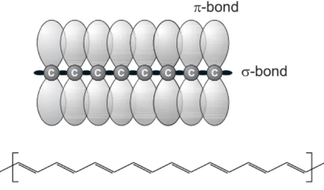
Organic photovoltaics are made of electron donor and electron acceptor materials rather than semiconductor p-n junctions. The molecules forming the electron donor region of organic PV cells, where exciton electron-hole pairs are generated, are generally conjugated polymers pos-sessing delocalized π electrons that result from carbonp orbital hybridization (see figure 1.1). These π electrons can be excited, by light in or near the visible part of the spectrum, from the molecule’s highest occupied molecular orbital (HOMO) to the lowest unoccupied molecular orbital (LUMO), denoted by a π−π∗ transition. The energy bandgap between these orbitals
determines which wavelength(s) of light can be absorbed [7].
CHAPTER 1. INTRODUCTION
Figure 1.1: Schematic representation of the electronic bonds between carbon atoms (above) and the
chemical structure of polyacetylene, comprising of alternating single and double bonds between the carbon atoms (below). Adapted from [10].
The conversion of photon energy into free charge carriers is explained by the following steps (also illustrated in figure 1.2, where the structure of a typical BHJ solar cell can be seen, followed by the correspondent energy-band diagram in figure 1.3):
• Light is absorbed in the donor material and thus excitons (i.e. strongly bound electron-hole pairs) are created in the polymer chain. Conjugated polymers have very high absorption coefficients, but, only narrow absorption bands, which can be circumvented by novel materials and/or multijunction (tandem cells) systems;
• The photogenerated excitons are strongly Coulomb bound due to the low dielectric constant in organic materials, and the correspondingly low screening length. These need to be dis-sociated and in order for that they need to reach an acceptor site, which is done only by diffusion. However excitons have very short diffusion lengths, reason why for the use of bulk-heterojunction solar cells, which consists of an intermixed system of donor and acceptor materials;
• If the acceptor material/molecule is energetically favorable (i.e. the energy gain is bigger than the exciton binding energy) dissociation takes place, sending an electron into the acceptor and leaving a hole in the donor polymer. A polaron pair is formed;
• This pair still needs to be dissociated (since it is still Coulombically bound). This time, dissociation is assisted by an electric field (composed of built in voltage, plus an applied voltage), therefore photocurrent strongly depends on applied voltage;
• Finally the electrons and holes are transported to the respective electrodes, driven by the electric field, and moved by the hopping transport process, where they can then be collected;
+ -+ +
-3 4
5 2
1
Substrate
LiF/Al
Active blend ITO/PEDOT:PSS
1. Exciton generation 2. Exciton diffusion Charge recombination 4. Charge transport
3. Charge dissociation
5. Charge collection
Organic Active Layer
Figure 1.2: Schematic layout of a typical bulk-heterojunction solar cell. A section of the active layer is
enlarged to illustrate the processes of light absorption and charge generation/collection.
CHAPTER 1. INTRODUCTION
h+
e
-Figure 1.3: Schematic energy-band diagram of a bulk-heterojunction organic solar cell. The solid lines
represent the energy levels of the donor, while the dashed lines represent the energy levels of the acceptor. Adapted from [11].
1.1.1 Carrier transport
Charge carrier transport properties are a important part of a solar cell characterization. The electron and hole transport should be measured separately and for this purpose, single carrier devices are often used. These are fabricated by selectively blocking the carriers of opposite sign by changing the work function of the relevant contacts. For hole-only (HO) devices, a high work-function metal like gold (Au) is used as top contact. As for electron-only (EO) devices, to suppress/block hole injection, one can use a thin oxide barrier, such as aluminum oxide (Al2O3)
for the bottom contact. A schematic representation of single carrier devices can be seen in 1.4. In such devices, a space-charge limited current (SCLC) is often observed. This is because when a semiconductor polymer layer is contacted by an ohmic contact that can readily inject a large number of charge carriers and another electrode that can extract these charges, the current flow will be limited by a buildup of space charge due to the low carrier mobility found in such materials. The total amount of charge carrier injected into the insulator is linearly proportional with the voltage. The current is given by the amount of charges multiplied by their velocity. Since both the amount of charges as well as the velocity (mobility × electric field) are linearly
proportional with the voltage, this results in a quadratic dependence of the current density on voltage. Considering only one charge carrier, the SCLC density flowing across a layer with thickness L is given by [12, 13]
JSCL=
9 8ǫµ
V2
int
L3 (1.1)
whereǫis the dielectric constant of the material (estimated to be 3 for organic semiconduc-tors),µthe carrier mobility andVintthe internal voltage in the device. Electrostatically there is a limit for the build up of space charge in a semiconductor when the integral of the space-charge induced field over the semiconductor thickness is equal to the applied voltage. Then, the SCLC is reached, which is the maximum current that can be sustained. The internal voltage drop
ß²±¼»æ ×ÌÑñÐÛÜÑÌæÐÍÍ
Ý¿¬¸±¼»æ ß« ó
õ
ײ¶»½¬·±² Ì®¿²-°±®¬
(a)Hole-only device
ß²±¼»æ Ô±©
©±®µº«²½¬·±² Ý¿¬¸±¼»æ Ô±©
©±®µº«²½¬·±² ó
õ ײ¶»½¬·±²
Ì®¿²-°±®¬
(b)Electron-only device
CHAPTER 1. INTRODUCTION
across the active layer is related to the applied voltage Va by
Vint=Va−Vbi−VRs (1.2)
whereVbiis the built-in voltage which arises from the difference in work function of the bottom and top electrode and VRs is the voltage drop across the series resistance of the substrate. The built-in voltage is determined from the J-V characteristics as the voltage at which the characteristic becomes quadratic, corresponding to the SCL regime. For organic semiconductors the SCLC equation 1.1 is only valid at low voltages. At higher voltages the charge carrier mobility increases with increasing electric field and carrier density,ρ. As a result the current is no longer quadratic with voltage, but increases more rapidly. In one of his works Pasveeret al.
[15] established a unified theoretical description of the fullT,ρ an E dependence of µ:
µ(T, ρ) =µ0(T) exp
1
2(σ
2
−σ)(2ρa3)δ
(1.3a)
µ(T) =µ0c1 exp
h
−c2σ 2i
(1.3b)
δ ≡2µ ln(σ
2
−σ)−ln(ln4)
σ2 , µ0≡
a2
v0e
σ (1.3c)
withc1 = 1.8×10⁻⁹ ,c2 = 0.42, and whereσ≡σ/kBT (σ represents the width of the Gaussian
distribution of localized states), a is the site spacing/lattice constant. This parametrization is particulary true for not too high densities.
1.1.2 Electronic trapping in organic semiconductors
In many organic semiconductors a big limiting factor is the presence of electronic traps. The exact origin of such trap states is still in debate, but the main proposed sources are impurities, structural defects, geminate pairs and self-trapping in intermolecular states [16]. Traps affect strongly the charge transport properties since trapped charge carriers do no longer take part in the charge transport. However, their columbic charge will influence the electric field distribu-tion in a device and therewith the transport. Further, if the release rate for trapped carriers is sufficiently low, there will be a significant time necessary to reach quasi-thermal equilibrium conditions. This causes delay and hysteresis effects in alternately operated devices. A prereq-uisite for trap free electron transport is that the LUMO should be deeper than 3.7 eV since electron trapping in organic semiconductors is universal and dominated by a trap level at ∼3.6
eV [17]. Therefore, having a LUMO level at ∼3.8 eV with PDI-1, should allow for trap-free
electron transport. Traps also act as recombination centers, being recombination of electrons
+ +
E
tE
vE
c(a) (b) (c) (d) (e)
Figure 1.5: Schematic representation of bimolecular recombination and the four processes involved in
recombination by trapping: (a) bimolecular, Langevin recombination, (b) electron capture, (c) electron emission, (d) hole capture, and (e) hole emission. Adapted from [18].
CHAPTER 1. INTRODUCTION
and holes, a process by which both carriers are annihilated. The main two mechanisms of re-combination are bimolecular and trap-assisted rere-combination, which are illustrated in figure 1.5. Bimolecular recombination (figure 1.5a), also known as non-geminate recombination, is usually considered to be of the Langevin-type. Direct band-band recombination of free carriers does not exist as such in organic disordered semiconductors, so, for two oppositely charged carriers to recombine, they first have to find each other [19, 20]. That is described by the Langevin re-combination rate. Trap-assisted rere-combination, i.e. Shockley-Read-Hall (SRH) rere-combination, is a two-step process where a trap state captures a charge carrier that subsequently recombines with a mobile carrier of the opposite sign due to their Coulombic interaction. This process is illustrated in figure 1.5b-d and is often described by the following recombination rate
RSRH = CnCpNtnp
Cn(n+n1) +Cp(p+p1)
(1.4a)
p1n1 =Ncv exp
−Egap
kT
(1.4b)
where Cn and Cp are the capture cross sections for electrons nand holes p, respectively. Ncv is the effective density of states;Ntis the density of electron traps; andp1n1follows the relationship
shown in equation 1.4b [18].
1.2
Device characteristics of organic solar cells
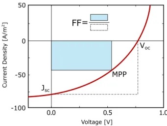
An organic solar cell based on conjugated polymers consists on, the later, being sandwiched between two electrodes with asymmetric work function. To determine the performance of a solar cell, the device is characterized in dark and under illumination. An example of a typical J-V curve of an organic solar cell can be seen in figure 1.6. From such graph a few important performance parameters can be extracted, mainly the open circuit voltage, short circuit current, fill factor, and maximum power. Open circuit voltage (Voc) is the maximum photovoltage the
cell can supply and is the voltage for which the current under illumination is zero. Similarly, the current that runs through the cell at zero voltage corresponds to the short circuit current (Jsc). Being power the product of current and voltage, the point of the curve where J ×V is
maximum, represents the maximum power output (Pmax). Finally, the fill factor (FF) is a way of
calculate the quality of theJ-V characteristic, and is given by the ratio ofPmaxand the product
MPP
Voc
Jsc
FF=
0
-50
-100 50
0.0 0.5 1.0
Cu
rr
e
n
t
D
e
n
s
it
y
[A
/m
2]
Voltage [V]
Figure 1.6: Typical current density-voltage characteristic of an organic bulk-heterojunction solar cell.
The characterization parameters Jsc, Voc, and FF are indicated. The maximum-power point (Mpp) is
also shown, where the maximum power Pmax that the solar cell can supply is represented by the filled
CHAPTER 1. INTRODUCTION
ofJsc×Voc. This parameters allow us then to determine the power conversion efficiency (PCE),
η, of the cell, which is given by the ratio between Pmax and the incident power, Pin:
η= Pmax Pin
= JscVocF F
Pin
(1.5)
1.3
Perylene Diimides
Perylene-3,4,9,10-tetracarboxylic acid diimide derivatives, also known as perylene diimides (PDIs), are n-type organic semiconductors and common non-fullerene acceptors used in OPVs. PDIs generally show high thermal, chemical, and light stabilities, good electron-accepting abilities due to the well placed LUMO energy, and excellent electron mobilities [21–24]. Compared to fullerenes, PDIs show a strong and broad absorption in the visible spectral region and their op-toelectronic properties are easily tuned by tailoring the substituents on the imide-N, bay, and/or non-bay positions (see figure 1.7). This makes PDIs promising candidates to replace fullerenes, however they have been falling short in terms of performance. Traditional PDI derivatives show over-strong aggregation, leading to formation of large (tens to hundreds of nanometers) crys-talline aggregate domains. In these structures, excitons decay into intermolecular states and the well-ordered PDI domains act as charge traps, severely limiting exciton diffusion/separation efficiencies and further the PCE of the devices [25]. To avoid over aggregation and PDI colum-nar stacking, non-placolum-nar PDI derivatives such as dimers [26] or star-shaped structures [27] are beginning to be used, which have demonstrated a certain increase in PCEs. However, much remains to be known about PDIs and their derivatives.
N
O O
R
R'
R''
N
O O
R
R:peri-function
solubility aggregation photostability
R':bay-function
optical electrochemical solubility
R'':orto-function
optical electrochemical solubility planarity
Figure 1.7: Illustration of the chemical structure of the PDI base structure and the possible positions
for the tuning of its properties.
Chapter 2
Materials and Methods
The work conducted in this dissertation involved the synthesis of different active layer solutions and fabrication and characterization of various organic solar cells. Following substrate cleaning, spin coating of the relevant blends and deposition of electrodes was done. Active layer films and final devices were morphologically and electrically characterized, respectively. This chapter summarizes relevant materials, techniques and software programs used.
2.1
Substrate Cleaning
The devices were fabricated on 3×3 mm, pre-patterned ITO coated glass substrates (OPVs
and hole-only) and non-coated ones (electron-only). The substrates were treated/cleaned with a sequential process of scrubbing with water and neutral soap for 6 minutes, 5 minute long ultrasonic baths (both in acetone and isopropanol) and 25 minutes of UV-Ozone. The entire above mentioned cleaning process was done in air, inside a ISO class 6 cleanroom.
2.2
Solution synthesis
2.2.1 Solution Solvents
Commercial Chlorobenzene (CB) and Chloroform (CF) were obtained from Sigma Aldrich. Their chemical structure can be found in the Appendix, auxiliary figure A1.
2.2.2 Donor and acceptor materials
Commercial regioregular poly(3-hexylthiophene-2,5-diyl) (P3HT) was purchased from Solarmer Materials Inc. Commercial Perylene Diimide (PDI) and Phenyl-C61-butyric acid methyl ester (PC61BM) were purchased from Sigma-Aldrich Co. LLC, and the PDI derivatives were supplied
by the group of Prof. Müllen, from the MPIP. For convenience, these materials will be from now on referred to as PDI-1 (commercial PDI), PDI-2, PDI-3 and PDI-4. The structure of the aforementioned materials can be found in auxiliary figure A2, with the exception of the PDI derivatives due to confidentiality reasons.
2.2.3 Active Layer Solution (P3HT:PDI and P3HT:PCBM)
For preparation of the active layer, P3HT and the relevant PDI derivative were dissolved in CF at different concentrations and ratios, and then both heated and stirred overnight in a nitrogen filled glovebox (with typical O2 and H2O levels below 1 ppm). Solutions were then filtered
through a PTFE syringe filter. P3HT:PCBM solutions were prepared in an identical fashion, in this case with a ratio of 1:1 and concentration of 30 mgml-1.
2.3
Device fabrication
2.3.1 Material deposition
CHAPTER 2. MATERIALS AND METHODS
Al4083) was filtered with a 0.45 µm filter directly onto the substrate and, unless otherwise noted, a standardized program was used to spin coat at 2500 rpm, in room temperature. After spin coating of this layer, the samples were annealed/dried in the oven at 140°C for 10 minutes. As for the active layers itself, right after filtering the prepared solution, spin-coating of the active layers was done inside a nitrogen filled glovebox.
2.3.2 Contact evaporation
Top and bottom metal contacts were deposited through a specific shadow mask for each of the two layers, which results in four active areas with 1 x 10⁻⁵ m2, 1
.5 x 10-5 m2, 3
.75 x 10-5 m2 and
9.95 x 10⁻⁵ m2. The device structure and sample layout of the single carrier devices and OPVs
are depicted in auxiliary figure A3. This process was conducted in a vacuum evaporator system (from Vactec LLC, auxiliary figure A4) under a typical pressure around 5 x 10⁻⁷ mbar. During
the evaporation process the sample were constantly rotated for improved layer uniformity. In electron-only (EO) devices, an aluminum (Al) anode layer, with a thickness of 30 nm is evapo-rated prior to spin-coating of the active layer, then left in outside air for 10 minutes to form an oxide layer of about 2-3 nm. Depending on the device (OPV, HO or EO), different top contacts were used. These consisted of either Barium/Aluminum (Ba/Al), Lithium Fluoride/Aluminum (LiF/Al) or Gold (Au). The Ba layer of 5 nm was deposited using a manual program at an initial rate of about 0.5 nm/s gradually moving up to 1 nm/s. Regarding the LiF layer, a total thickness of 1 nm was also deposited via a manual program, with a rate of about 0.1 to 0.2 nm/s. Aluminum and gold were deposited with an automatic program, both for a thickness of 100 nm. The programs starts with a low rate and ends with a rate of 1 nm/s.
2.3.3 Thermal Annealing
Thermal annealing of the devices, was performed on a hot plate inside a glovebox, either before top contact evaporation (pre annealing) or after (post annealing).
2.4
Device characterization
2.4.1 Atomic force microscopy (AFM)
Surface morphology characterization of the PDI as-spun and annealed films, was performed by Atomic Force Microscopy (Veeco Digital Instruments, DI 3100 Cl, standard tip 300 KHz).
2.4.2 Electrical characterization
Two different setups were used for electrical measurements of the devices fabricated. Current-voltage (I-V) curves, external quantum efficiency (EQE) and density filter measurements were done in nitrogen ambient using a Glovescan system from ECN. The other setup consists of a prototype system (see auxiliary figure A5) put together by technicians from MPIP, where is possible to measureI-V curves while controlling the temperature via liquid nitrogen. This way, is possible to perform temperature scans on the single carrier devices. To be noted that all measurements, for stability and degradation reasons, were done in the same day of fabrication.
2.4.3 Simulation
To model the measuredJ-V characteristics of the fabricated single carrier devices, two computer programs were used. The first only uses the Mott-Gurney’s law for space-charge limited current in a trap free intrinsic semiconductor (equation 1.1). The second is a pascal computer software, SIMsalabim 2.7, where Pasveer’s unified description of charge carrier mobility (equation 1.3a, which takes into account temperature, carrier density and electric field) and other models are available to fit the experimental data.
Chapter 3
Results and Discussion
This chapter presents the different experiments made and the discussion of the associated results. These will be divided into three parts: in section 3.1, P3HT:PCBM solar cells are fabricated and characterized to serve as reference cell; chapter 3.2 addresses the main focus of the work of charge carrier transport properties of a commercial PDI acceptor material in single carrier devices and solar cells based; in chapter 3.3, novel PDI derivatives, supplied by the group of Prof. Müllen, from the MPIP, are also tested in single carrier devices.
3.1
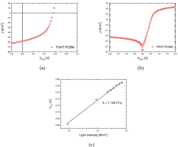
P3HT:PCBM system
P3HT/PCBM BHJ solar cells were fabricated to serve as a reference in our working condi-tions (equipment, material batches, processing methods, etc.). Literature results for optimized P3HT/PCBM systems, without any additive or additional layers, report PCE values of around 2-4 % [28, 29].
Solar cells were made, using a solution blend of P3HT:PCBM (1:1 wt/wt) in chloroform with a concentration of 30 mgml-1. PEDOT:PSS and the active layer solution were spin coated at
500 rpm and 3000 rpm for a layer thickness of 60 nm and 300 nm, respectively. The devices were topped off with a LiF/Al cathode. The measured J-V characteristics under light and in dark are shown in figures 3.1a, 3.1b. The cells were measured with an input power Pin of about
890 W/m2. The P3HT:PCBM solar cells had an maximum values for
Voc and Jsc of 0.56 V
and 58.08 A/m2, respectively, resulting in a FF of 49.74 % and a maximum PCE of 1.815 %
(see table 3.1 for full average metrics). These results seem to fall short in terms of performance compared to above mentioned optimized systems of P3HT:PCBM cells from literature, although to confirm their exact active area values would have to be known and considered.
One of the main performance-limiting mechanisms in many organic bulk-heterojunction so-lar cells is non-geminate recombination of separated charge carriers. Thus, understanding the recombination mechanisms of separated charge carriers is crucial to design strategies to re-duce non-geminate recombination [30]. A particularly important indicator of the recombination mechanism is the so-called ideality factor. An ideality factor of 1 indicates a bimolecular recom-bination, whereas an ideality factor of 2 implies that monomolecular recombination (Shockley-Read-Hall recombination, i.e. trap-assisted recombination) is dominant [31]. One way to obtain the ideality factor is by calculating the slope of the exponential regime for the dark J-V char-acteristics at forward bias, and that can be expressed as [32]
η=kT q
∂lnJd ∂Vbias
−1
(3.1)
where kT is the thermal energy, Jd is the dark current and Vbias the applied voltage. In P3HT:PCBM solar cells, the darkJ-V characteristics under forward bias are expected to show typical diode behavior: leakage contribution at low voltages, exponential regime at intermediate voltages and space charge limited current after the built-in voltage (Vbi). Unfortunately theJ-V profile of the dark current under forward bias, of the fabricated P3HT:PCBM OPVs, did not allow for a calculation through this method.
An alternative way to determine the ideality factor is to use the light intensity andVoc instead
CHAPTER 3. RESULTS AND DISCUSSION
VBias [V]
-0.2 0.0 0.2 0.4 0.6 0.8 1.0 -80 -70 -60 -50 -40 -30 -20 -10 0 10 20 J [ A /m 2] P3HT:PCBM (a)
-2.0 -1.5 -1.0 -0.5 0.0 0.5 1.0 1.5 2.0 10-5 10-4 10-3 10-2 10-1 100 101 102 103 104 P3HT:PCBM J [ A /m 2]
VBias [V]
(b)
101 102 103
0.66 0.68 0.70 0.72 0.74 0.76 0.78 0.80 VO C [ V ]
Light intensity [W/m2
] S = 1.138 kT/q
(c)
Figure 3.1: J-V characteristics of P3HT:PCBM (1:1 wt/wt) solar cells (a) under light and (b) in dark.
(c) Voc vs light intensity of the same solar cells.
Table 3.1: Average metrics of the P3HT:PCBM (1:1 wt/wt) solar cells. For the study of this system 3
devices were characterized.
Device system Thickness [nm] VOC [V] JSC [A/m2] FF [%] PCE [%]
P3HT:PCBM (1:1) 300 0.56±0.01 38.96±19.12 51.76±2.67 1.26±0.55
photogenerated charge carriers recombine. This implies that the open-circuit voltage is limited by the amount of recombination that is present in the device. Therefore, a reduction in the recombination strength would lead to a higher open-circuit voltage. Because the generation rate is proportional to the light intensity, the dependence of the Voc on the light intensity can be a
more reliable and sensitive method to determine the recombination mechanisms present in the solar cells [33], compared to calculating it through the dark current. The open-circuit voltage can be expressed as
Voc=
Egap
q −
kT q ln
(kR)N2
c G
!
(3.2)
with Egapthe energy gap between the HOMO of the acceptor and the LUMO of the donor, kR the bimolecular recombination coefficient, N2
c the density of states, and G the generation rate of excitons.
Plotting the Voc values as a function of the natural logarithm of light intensity, a slopekT /qof
CHAPTER 3. RESULTS AND DISCUSSION
roughly 1.2 is obtained, as depicted in figure 3.1c. This can be interpreted as an ideality factor of ∼1.2, pointing to the absence of deep traps and to recombination being mostly bimolecular.
However, fitting a straight line to a Voc vs light intensity plot, resulting in a slope of one could
be from averaging over different recombination mechanisms. At the same time, ideality factors from dark currents that often are much larger than one, are no proof of trap-assisted recom-bination as it can be caused by resistive effects [33]. Therefore, in order to get a more precise ideality factor, further experiments have to be done, where the the latter is retrieved from the light output of the solar cell (when stressed).
3.2
Donor:PDI systems
3.2.1 AFM characterization of PDI films
CHAPTER 3. RESULTS AND DISCUSSION
0 µm 2 4 6 8 10 12 14 16 18 0 2 4 6 8 10 12 14 16 18 398 nm 0 50 100 150 200 250 300 350 (a)
0 µm 2 4 6 8 10 12 14 16 18 0 2 4 6 8 10 12 14 16 18 335 nm 0 50 100 150 200 250 300 (b)
0 µm 2 4 6 8 10 12 14 16 18 0 2 4 6 8 10 12 14 16 18 352 nm 0 50 100 150 200 250 300 (c)
Figure 3.2: AFM pictures of pristine PDI-1 films annealed for 30 min at (a) 50°C, (b) 60°C and (c)
80°C.
PDI-1 in chloroform
Figure 3.2 shows the surface topography, measured by AFM, of pristine PDI films cast from chloroform. The films were annealed for 30 min at different temperatures to observe the effect on PDI aggregation. The AFM images of the pristine PDI-1 films, show several micrometer large crystalline structures. Thermal annealing temperatures were not far apart, however there is a slight increase of the PDI-1 crystal size and their packing (increased crystal density). In all cases the domains are clearly separated from each other by distinct grain boundaries which are known to limit the charge carrier transport in thin layers [35].
P3HT:PDI-1 (1:1 wt/wt)
It has been reported that the D/A blend morphology can be controlled by the solvent from which the blend is spin-coated, to try and minimize large-size phase separation and/or enhancing polymer chain packing [36, 37]. Figure 3.3 shows the surface topography, measured by AFM, of films cast from a P3HT:PDI-1 blend in CF and in CB. From figure 3.3a it can be seen a large phase separation between the P3HT and PDI and large PDI-1 crystals is observed for the CB-processed P3HT:PDI-1 (1:1 wt/wt) blend film. The large PDI-1 crystals results in also large P3HT domains in between the PDI-1 crystalline particles. In the case of the P3HT:PDI-1 blend film processed from CF, shown in figure 3.3b, the phase-separation and PDI crystal formation is significantly reduced. This difference is due to the fact that CB has a higher boiling point than CF, which results in a slower evaporation rate compared to that of CF. Thermal annealing at 100°C of the films processed from CF (figure 3.3b), leads to the appearance of ribbon-like elongated features.
CHAPTER 3. RESULTS AND DISCUSSION
(a)
0 µm 2 4 6 8 0 2 4 6 8 7.76 nm 2.33 3.00 3.50 4.00 4.50 5.00 5.50 6.00 6.50 7.00 7.50 (b)
0 µm 2 4 6 8
0 2 4 6 8 39.7 nm 0.8 5.0 10.0 15.0 20.0 25.0 30.0 35.0 (c)
0 µm 2 4 6 8 0 2 4 6 8 80 nm −0 10 20 30 40 50 60 70 (d)
Figure 3.3: AFM height images of P3HT:PDI-1 blend films with different PDI fraction, cast from
CB and CF, non-annealed and annealed. (a) As-spun P3HT:PDI-1 (1:1 wt/wt) film cast from CB; (b) As-spun P3HT:PDI-1 (1:1 wt/wt) film cast from CF; Annealed (10 minutes at 100°C) P3HT:PDI-1 (1:1 wt/wt) film cast from CF; and annealed (10 minutes at 100°C) P3HT:PDI-1 (1:4 wt/wt) film cast from CF.
The change of PDI fraction apparently yields no big change in the microstructure of the film. Increasing the PDI-1 content in the blend to 1:4 (P3HT:PDI-1) results in a slight bigger density of PDI-1 crystals but its average size stays virtually the same (figure 3.3d).
Cross-sectional scanning electron microscopy (CS-SEM) characterization of the P3HT:PDI-1 films would be needed to assess vertical phase separation and the creation of the necessary network for the charge carrier percolation pathways.
3.2.2 MEH-PPV:PDI-1
Solar cells and electron-only devices were fabricated using MEH-PPV as donor material. PE-DOT:PSS and an active blend solution of MEH-PPV:PDI-1 (1:4 wt/wt) in chloroform (16.67 mgml-1), were both spin coated at 1200 rpm, for a layer thickness of 50 nm and 260 nm,
respec-tively. Devices were toped off with a Ba/Al cathode and post annealed for 10 min at 110°C. The solar cells were measured with aPinof about 890 W/m2. The measuredJ-V characteristics
under light and in dark are shown in figure 3.4, for both non-annealed and annealed devices. Upon annealing, the solar cells show an increase ofJsc, of roughly 1.25 fold, whileVocremained
unchanged at ∼0.79 V, resulting in an average PCE of 0.022 %. Not annealed devices had an
average PCE of 0.017 %. The device metrics are summarized in table 3.2. As can be observed in figure 3.4b, the dark J-V characteristics show typical diode behavior for forward bias and by using equation 3.1, we obtain an ideality factor of ∼2 and ∼1.8 from the dark current, of
the non-annealed and annealed devices, respectively. In contrast, the slope S of theVocvs light
intensity characteristics of the non-annealed solar cells gives an ideality factor of roughly 1.1 (see figure A6). As mentioned before, is difficult to draw conclusive observations from ideality factors retrieved from the solar cells current, however the results fromVoc dependence on light
CHAPTER 3. RESULTS AND DISCUSSION
-0.2 0.0 0.2 0.4 0.6 0.8 1.0 -1.6 -1.2 -0.8 -0.4 0.0 0.4 J [ A /m 2 ]
VBias [V]
Non-annealed Post annealed
(a)
0.4 0.6 0.8 1.0 1.2 1.4 1.6 1.8 2.0 10-5 10-4 10-3 10-2 10-1 100 101 102
0.60 0.65 0.70 0.75 0.80 0.0 0.5 1.0 1.5 2.0 2.5 3.0 3.5 4.0 (k T /q ∂ ln J / ∂ V ) -1 VBias [V] Non-annealed Post annealed J [ A /m 2]
VBias [V]
(b)
Figure 3.4: J-V characteristics for the non-annealed (blue) and post annealed (red) MEH-PPV:PDI-1
(1:4 wt/wt) devices (a) under light and (b) in dark. The inset of (b) shows the differential plot of the data according to equation 3.1.
Table 3.2: Average metrics of the MEH-PPV:PDI-1 (1:4 wt/wt) non-annealed and post annealed
so-lar cells, with a active layer thickness of ∼260nm. For the study of this layer system 3 devices were characterized.
MEH-PPV:PDI-1 (1:4) VOC [V] JSC [A/m2] FF [%] PCE [%]
Non-annealed 0.78 ±0.01 0.49 ±0.18 39.73 ±1.97 0.017±0.007
Post annealed 0.80 ±0.01 0.62 ±0.22 39.60 ±0.89 0.022±0.007
Electron-only devices have been fabricated. Measuring theirJ-V characteristic and then fitting the data with the SCLC model, the parameters of the electron mobility can be determined. Repeating the process using the drift-diffusion model from Pasveer, for different temperatures, the temperature dependency of the mobility can be found, as well as an approximation of the site spacing and energetic disorder of the active blend. The electron-only currents, before and after post annealing, are plotted as a function of the applied voltage, and are presented in figure 3.5a. There is a slight different injection behavior from each electrode, however, for the voltage range used, both seem to show ohmic currents. Electron injection appears to be higher from (Al2O3) as compared to injection from the Ba/Al electrode. In a log-log plot of current density
vs voltage, an ohmic behavior results in a slope of 1, while SCLC gives a slope of 2. As observed in figure 3.5b a slope of approximately 1 is observable, confirming therefore, an ohmic regime for the range of applied fields. Ohmic currents in undoped semiconductors are often a result of the diffusion of charge carriers present in the metal contacts [38]. However this effect should not be noticeable for such a thick active layer (260 nm), which leads to believe that we have unwanted doping. Upon thermal annealing, current density of the EO device decreases slightly, probably due to the removal of the just mentioned dopants.
A current that follows Ohm’s law is described by the following expression
J =qp0µ
V
L (3.3)
where p0 is the background charge carrier density. However, looking at the temperature scan
in figure 3.6, the J-V characteristics of the EO device show a clear and significant temperature dependency. To verify the presence of a SCLC in the device, re-measuring of the J-V
CHAPTER 3. RESULTS AND DISCUSSION
-2.0 -1.5 -1.0 -0.5 0.0 0.5 1.0 1.5 2.0 10-2 10-1 100 101 102 J [ A /m 2]
VBias [V]
Non-annealed Post-annealed
(a)
10-2 10-1 100
10-3 10-2 10-1 100 101 102 J [ A /m 2]
VBias [V]
Electron-only (reverse bias)
Linear fit
(b)
Figure 3.5: (a) ExperimentalJ-V characteristics (symbols) of a non-annealed (blue) and annealed (red)
MEH-PPV:PDI-1 (1:4 wt/wt) EO device and (b) again of a non-annealed device at reverse bias. The solid line is an automatic linear fit to the experimental data with slope 1.
teristics at higher voltage values is required. Once the electron mobility is determined we can then predict the charge carrier concentration through equation 3.3.
-2 -1 0 1 2
10-5 10-4 10-3 10-2 10-1 100 101 102 J [ A /m 2 ]
VBias [V] 293 K
273 K 253 K 233 K 213 K
Figure 3.6: Temperature-dependent J-V characteristics of a non-annealed EO device with a
MEH-PPV:PDI-1 (1:4 wt/wt) active layer system.
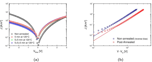
3.2.3 P3HT:PDI-1
PDI-1 has been rather used previously in other literature works, however much remains to be known about its electronic properties, namely charge transport, in PDI-based OPVs. To study the behavior of PDI when blended with P3HT, devices with an active layer of P3HT:PDI-1 have been fabricated. Solar cells and EO devices were made, using a solution blend of P3HT:PDI-1 (1:1 wt/wt) in chloroform with a concentration of 10 mgml-1. PEDOT:PSS and the active blend
CHAPTER 3. RESULTS AND DISCUSSION
-3 -2 -1 0 1 2 3
10-3 10-2 10-1 100 101 102 J [ A /m 2]
VBias [V]
Non-annealed 5 min at 120°C 5+5 min at 120°C 5+5+5 min at 120°C
(a)
10-1 100
10-3 10-2 10-1 100 101 J [ A /m 2] V -V bi [V]
Non-annealed(reverse bias)
Post-Annealed
(b)
Figure 3.7: (a) ExperimentalJ-V characteristics (symbols) before and after three consecutive annealing
steps of 5 min at 120°C of a P3HT:PDI-1 (1:1 wt/wt) EO device, with a layer thickness of about 120 nm. (b) Fitting (solid lines) of the non-annealed (blue)(reverse bias) and post annealed (red) EO devices, calculated using equation 1.1. For the non annealed device aVbi of 0.12 V was used.
significant reduction in current density upon the first 5 minutes of annealing. A possible reason is that in the non-annealed devices, there are already present impurities (i.e. positive ions) that will contribute in the charge transport and/or that the thin oxide layer does not provide a big enough barrier to fully block hole injection from the Al contact. When the device is annealed, interfacial states are removed and structural rearrangement takes place at the interface. On the other hand, electron injection from from the Ba/Al side increases upon annealing (at lower applied fields) and, overall, a more balanced electron current across the whole device is obtained. For all further annealing steps, the measured current densities were practically the same, only showing a minimal decrease on the Al2O3 side.
In figure 3.7b, the electron-only currents are plotted as a function of the applied voltage (cor-rected for the built-in voltage Vbi), and fitted accordingly. These currents can be well described by equation 1.1 for SCLC, exhibiting a quadratic dependency on voltage. The electron mobil-ity values obtained from such model, for the non-annealed (at reverse bias) and annealed (at forward bias) devices, were 4.5 x 10⁻¹¹ m2
/Vs and 1.7 x 10⁻¹¹ m2
/Vs, respectively. However, this model doesn’t take into account charge carrier density and electric field variations. Therefore, without measuring the J-V characteristics and fitting them for a range of different layer thick-nesses (minimum 3), there is no way to confirm that the currents are fully bulk limited and the presented electron mobilities, which can only be considered an approximation and are predicted to be considerably lower.
Figure 3.8 shows the temperature dependent J-V characteristics of an EO device, before and after post annealing. The best fit of the experimental data was obtained using the values expressed in table 3.3. The mobility retrieved from the unified description of Pasveer, was 3.17 x 10⁻¹³m2
/Vs and 3.67 x 10⁻¹³ m2
/Vs, respectively for non-annealed and post annealed de-vices. For the full range of voltage and temperatures used, the modeling describes very well the experimentalJ-V characteristics, although regarding the post annealed EO devices, the current tends to be more ohmic than space-charge-limited at lower applied fields. This phenomenon has been described and is related to the movement of the virtual cathode (the point of zero electric field) as a function of voltage [39]. Nevertheless, the good agreement of the current-voltage characteristics with eq.1.1 in the low field regime and the accurate description of the tempera-ture dependent currents with the drift-diffusion model are strong indications that the electron transport is essentially trap free.
Figure 3.9, shows the electron and hole current densities of non-annealed P3HT:PDI-1 (1:1 wt/wt) EO and HO devices with a layer thickness of 210 nm. Again they exhibit a quadratic
CHAPTER 3. RESULTS AND DISCUSSION
Table 3.3: Fit parameters used for modelling the temperature-dependentJ-V characteristics of a
non-annealed and non-annealed P3HT:PDI-1 (1:1 wt/wt) EO device with a layer thickness of 120 nm.
Device µ0(295 K) Mobility pre-factor Width of Gaussian,σ Site spacing, a Φleft/right Vbi
Non-annealed 3.17 x 10⁻¹³m2
/Vs 1600 0.158 eV 1.7 nm 0/3 eV 0.12 V
Post annealed 3.64 x 10⁻¹³m2
/Vs 500 0.148 eV 1.2 nm 0/3 eV 0 V
dependence on voltage and can be well fitted using equation 1.1. We observe a difference of about two orders of magnitude between the electron and the hole current. This is evidence of a pronounced unbalanced charge transport and that holes are clearly the dominant charge carrier in the P3HT:PDI-1 (1:1 wt/wt) blend.
TheJ-V characteristics under light and dark of a non-annealed and post annealed P3HT:PDI-1 (1:1 wt/wt) solar cell can be seen in figure 3.10. These devices were measured with a Pin of
about 1460 W/m2. The summarized solar cell metrics are found in table 3.4.
The non-annealed devices exhibit a leakage current regime at low applied forward bias which is not visible anymore in the post annealed ones. This is most probably due to the above mentioned removal of an interfacial barrier (from structural arrangement or presence of interfacial states) with the contacts, upon thermal treatment. However at the same time, this causes saturation current at reverse bias to increase. This reducing of interfacial barrier can also be visible in the decrease of Voc in theJ-V characteristics under illumination, as observed in figure 3.10a. Here
we can see that the Jsc of the solar cells is improved by roughly 6.5 fold, while Voc decreased
by 1.5 fold. Considering that the electron-mobility decreases with annealing, the performance improvement (due to a higher Jsc) of the OPVs, could be associated to the more balanced
electron current density (as a result from improved lateral phase separation) removal of an interfacial barrier that promotes charge collection and/or even hypothetically to an increase of the hole mobility upon annealing. Measuring of theJ-V characteristics of an annealed HO device would be needed to verify this last sugestion. The average fill factor values for not annealed and annealed P3HT:PDI (1:1 wt/wt) solar cells, are 33 % and 28 %, respectively. These low FFs can be mainly explained by the large difference in charge carrier mobilities (i.e. unbalanced transport) (evidenced in figure 3.9), which causes accumulation of space charges and increased recombination [20, 40–42].
As depicted in figure 3.10c, the slope S of theVocvs light-intensity characteristics equals 0.9 and
2 for the non-annealed and post annealed devices. This can be interpreted as ideality factors of
10-1 100
10-5 10-4 10-3 10-2 10-1 100 101 102 295 K 275 K 255 K 235 K 215 K J [ A /m 2]
V - Vbi [V]
(a)
10-1 100
10-5 10-4 10-3 10-2 10-1 100 101 295 K 275 K 255 K 235 K 215 K J [ A /m 2]
VBias [V]
(b)
Figure 3.8: Temperature dependent experimental J-V characteristics (symbols) of P3HT:PDI-1 (1:1
CHAPTER 3. RESULTS AND DISCUSSION
Table 3.4: Average metrics of the P3HT:PDI-1 (1:1 wt/wt) non-annealed and annealed devices, with a
layer thickness of ∼120 nm. For the study of this system 4 devices were characterized.
P3HT:PDI-1 (1:1) with LiF/Al VOC [V] JSC [A/m2] FF [%] PCE [%]
Non-annealed 0.521±0.10 1.04 ±0.14 32.99±4.64 0.012 ±0.005
Post Annealed 0.350±0.01 6.07 ±2.12 28.16±1.00 0.041 ±0.016
unity and 2, indicating that in non-annealed solar cells recombination is trap-assisted (i.e. SHR, band to band recombination), associated to the just above mentioned pronounced unbalanced transport between electrons and holes which causes recombination to be driven/limited by both carrier types.
P3HT:PDI-1 (1:1 wt/wt) solar cells with a Ba/Al cathode, have also been made. PEDOT:PSS and the active blend solution were spin coated at 2500 rpm and 1200 rpm resulting in a layer thickness of 40 nm and 80 nm, respectively. Both pre annealing and post annealing of the devices was done, for 15 minutes at 100°C. These devices were measured with a Pin of around
890 W/m2. The
J-V characteristics under light and dark of the non-annealed, pre annealed and
Table 3.5: Average metrics of the P3HT:PDI-1 (1:1wt/wt) devices with a Ba/Al cathode and an active
layer thickness of 80 nm. For the study of the systems 3 devices were characterized.
P3HT:PDI-1 (1:1) with Ba/Al VOC [V] JSC [A/m2] FF [%] PCE [%]
Non-annealed 0.44±0.04 0.45±0.16 27.99±0.91 0.006 ±0.003
Pre Annealed 0.26±0.03 1.64±1.01 30.76±4.00 0.015±0.01
Post Annealed 0.28±0.01 2.52±0.60 29.48±1.65 0.023 ±0.006
post annealed devices can be seen in figure in 3.11b, as well as a summary of their main figures of merit, in table 3.5. Pre annealed devices show a Jsc of 1.643 A/m2, significantly lower
than 2.519 A/m2 of the post annealed ones. On the other hand, both pre annealed and post
annealed OPVs, have a similar decrease ofVocof around 1.6 fold, which means that the thermal
10-1
100
10-3
10-2
10-1
100
101
102
103
J
[
A
/m
2 ]
V - Vbi [V] Hole-only
Electron-only (reverse bias)
Figure 3.9: ExperimentalJ-V characteristics (symbols) of a P3HT:PDI-1 (1:1 wt/wt) EO (red)(reverse
bias) and HO (blue) device, with layer thickness of∼210 nm. The solid lines are fits to the experimental data, calculated with eq.1.1 for SCL currents. For the electron-only device, a Vbi of 0.35 V was used.
![Figure 1.4: Schematic energy level diagrams in single carrier devices. Both are under forward bias [14].](https://thumb-eu.123doks.com/thumbv2/123dok_br/16697316.743869/19.892.175.711.952.1124/figure-schematic-energy-diagrams-single-carrier-devices-forward.webp)