ISSN 1517-7076 artigo 11697,pp.252-259, 2016
Autor Responsável: Marco Antonio Rodriguez Martinez Data de envio: 27/04/2015 Data de aceite: 25/09/2015
10.1590/S1517-707620160001.0023
Characterization of copper microelectrodes,
following a homemade lithography,
technique,
and gold electroless deposition
Marco Antonio Rodriguez Martinez 1,2, Lizbet Leon Felix 1, 2, Luis de los Santos Valladares 3, Angel Bustamante Dominguez 2,
Jose Antonio Huamani Coaquira 1, Jorge Rojas Alvarado2, Yutaka Majima 4, Jose Albino Aguiar 5, Crispin Barnes 3
1Núcleo de Física Aplicada, Instituto de Física, Universidade de Brasília, Brasília, DF 70910-900, Brazil. e-mail: [email protected]
2Laboratorio de Cerámicos y Nanomateriales, Facultad de Ciencias Físicas, Universidad Nacional Mayor de San Marcos, Ap. Postal 14-0149, Lima, Perú.
3Cavendish Laboratory, Department of Physics, University of Cambridge, J.J. Thomson Avenue, Cambridge CB3 0HE, United Kingdom.
4 Materials and Structures Laboratory, Tokyo Institute of Technology, Nagatsuta-cho, Modori-ku 4259-R3-5, Kanagawa 226-8503, Yokohama City, Japan.
5 Laboratório de Supercondutividade e Materiais Avançados, Departamento de Física, Universidade Federal de Pernam-buco 50760-901, Recife, Brazil.
e-mail: [email protected], [email protected], [email protected], [email protected], [email protected], [email protected], [email protected], [email protected]
_______________________________________________________________________________________ ABSTRACT
We report the fabrication and characterization of copper microelectrodes obtained by a homemade lithography technique and after gold electroless deposition. For the fabrication, planes consisting of arrays of electrodes (black in color) with bow tie shape were designed and printed on a transparent paper (Canson ltd.). Using an embroidery frame with a silk fabric, a photographic emulsion was spread on the silk and simultaneously press-ing the Canson paper on it. The system was introduced into a closed box and exposed with a UV light. The designed electrode templates prevented direct exposition of the UV light over copper films and indelible ink was spread over it. After the ink was dried, the copper film is immersed into ferric acid to attack the uncovered copper parts (where there is no ink). In this way, we obtained copper electrodes with initial gap separation of ~142μm and subsequently, they followed electroless deposition of gold to make the copper electrodes to con-tact. For the characterization, electrical measurements were performed. They present ohmic resistance values in the order of 106Ω produced by surface scattering of the electrons within the gold microwire and enhanced by oxidation of the copper electrodes.
Keywords: copper microelectrodes, electroless deposition, ohmic behavior, oxidation process.
_______________________________________________________________________________________
1. INTRODUCTION
253 surface, the most preferable is gold [17] since it allows the deposition of other different metals because it is a good conductor and it prevents oxidation. Nevertheless, other cheaper materials, such as copper, have not been much investigated for growing nanogaps electrodes.
In this work we report a homemade lithography technique for the fabrication of copper electrode pairs and their electroless deposition with gold. We have achieved gold deposition on the cooper electrodes surface until a contact is formed. We demonstrate that it is possible to electroless deposit gold on copper electrodes and to put them into contact. This happened in spite that the initial distance gap obtained by our homemade lithography is thousand times larger than the average distance achieved by other sophisticated techniques [12]. In addition, our technique allows fabricating relative large area electrodes (3.2cm x 2.2cm) than common li-thography (1 x 1mm2) [12,19]. In our case, the area of the electrodes can be reduced by fine and selected cuts. Technological advantages lie in having obtained micro gaps that can be used to place micro or macromolecules. Also nanogaps could probably get through the application of techniques for breaking our microwire as is the electromigration-induced break junction (EIBJ technique).
1. MATERIALS AND METHODS
1.1 Fabrication of initial electrodes by a homemade lithography
We have performed a homemade lithography process without the use of any sophisticate equipment. With the help of the Corel Draw software, planes of array of electrodes with bow tie shape (5 cm × 4 cm) were designed. The planes were printed on a transparent paper (Canson ltd.) to allow transmittance of the natural light through it. Using an embroidery frame with a silk fabric divided into 100 to 150 lines per inch, the electrode paths were painted. We used a photo-sensible green film made by the company Rednora, which allows exposure range from 365 to 400 nm and with thickness of 40 micrometers and a resolution of 60 micrometers. This film hardens when it is exposed to UV. The photosensible film is spread across the surface of the silk fabric, and the Canson paper was pressed over this. Then the silk fabric and the Canson paper with the film between them were intro-duced into a closed box in which a UV light source exposed the system around 10 to 15 minutes as shown in Figure 1(a). The black printing designs of the electrodes prevent exposition of the UV light over them. In fact, this color has a quite high absorption coefficient and does not allow the passage of UV rays; therefore, these parts are removed easily leaving the design on the silk fabric as shown in Figure 1(b).
254 Figure 1: a)-d) Schematic representation of the homemade lithographic technique process to obtain copper microgaps electrodes and e) their electroless deposition with gold.
1.2 Electroless gold deposition
The gold electroless deposition technique of the electrodes is described in detail in a previous work [16] with some modifications in the electrolyte composition and the steps followed during the plating process. In brief, the electroless plating solution was based on a combination of iodine tincture, gold, and L(+)-ascorbic acid. Iodine tincture reacts with gold film to form [AuI4]- and the ascorbic acid reduces excess I-3 to I- and the Au (III) complex to Au on the Cu surface [17]. During this process, some gold crystals of different sizes remain undissolved in the electrolyte. Some images of these undissolved gold particles are shown in Fig. 2. Since Cu2O and CuO are formed on Cu surfaces in ambient conditions [20], prior electroless deposition the Cu elec-trodes were immersed into 10 ml of hydrochloric acid (HCl), with concentration of 2.5%, for 30 s so as to remove these Cu-oxides. We also observed that higher concentration of HCl promotes etching of the copper film. Immediately, the electrodes were rinsed with distilled water following dropping the plating solution di-rectly to the gap electrodes (as shown in Fig. 1(e) above).
1.3 Characterization
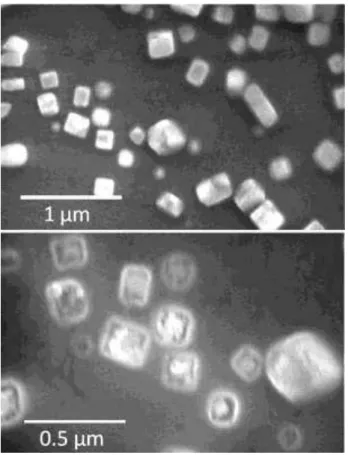
255 Figure 2: Scanning electron micrographs (at two magnifications) of some undissolved gold crystals used for the electroless platting.
2. RESULTS AND DISCUSSION
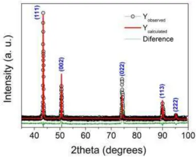
Figure 3 shows the X-ray diffraction patterns of the copper electrodes taken after HCl washing and prior gold electroless plating. All Bragg reflections in the XRD are consistent with the cubic structure of the copper phase (space group,
Pm
3
m
), excluding the occurrence of Cu-oxides. In order to estimate the particle size, the XRD pattern was refined by using the Rietveld method. The particle size (D) is related to the line-width (Γ) by the Scherrer equation: D0.916
/cos
hkl, where
is the wavelength of the X-rays (0.15418 nm), andhkl
256 Figure 3: XRD patterns of the initial copper electrodes. The observed and calculated data are represented by the points and solid line, respectively. The calculation was performed by following the Rietveld method. The difference between the observed and calculated data is also plotted (green lines).
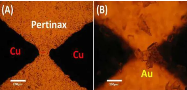
Figure 4 shows optical microscope images of the superficial morphology of the copper electrodes before and after gold electroless plating. Fig. 4(A) shows the Cu electrodes after HCl bathing (before electroless plat-ing). It is demonstrated that our homemade lithographical technique is effective to obtain copper electrodes of 1 mm thickness forming gaps up to 142.38 μm and without the use of any sophisticate equipment. After gold electroless deposition (Fig. 4(B)), we observe parallelepiped gold crystals bridging the copper electrodes. The gold crystals have different sizes (from 50 nm to 10 µm, see also Fig. 2) µm and we observed that up to three crystals arrange vertically, thus the thickness of the gold coating is in the interval 1-100 µm. Our research group is currently investigating the improvement of the technique to obtain a more uniform electroless platting. The adherence of the gold coating on the copper substrate was confirmed by washing the samples in H2O and C3H7OH several times.
257
Figure 4: Optical images of a typical sample obtained by our homemade lithographical technique before (A) and after (B) electroless gold plating.
Figure 5 shows the I-V measurements performed by the four probe method at room temperature of one arbitrary pair of copper electrodes bridged with gold crystals. It is well known that the conductance of a wire is inversely proportional to its length and that the electron transport mechanism depends of length scale. In the present work, the length (L) of the gold microwire formed between the copper electrodes is ~ 142μm and comparing to his respective mean free path (ℓ) at room temperature, we obtain that L >> ℓ which means it consists on a diffusive electron transport [23]. This is confirmed by the ohmic trace obtained in the devices in this work (see Fig. 5). It gives a resistance of 286.65 MΩ with a conductance of 3.48 nS.
258 Figure 5: a) I-V measurement of the sample after gold deposition. The calculated resistance is 286.65 MΩ and the dimen-sions of the gold microwire bridge is 142,38μm (L). b) I-V characteristic of a typical sample obtained by homemade litho-graphic technique and after electroless gold deposition (scan voltage up to 10 V). Inset: Scan voltage up to100V.
3. CONCLUSIONS
We have successfully demonstrated a homemade lithographic technique for the production of Cu electrodes with gap separation as less as 100 µm. This technique is cheap and does not require the use of sophisticate apparatuses. Moreover, we have achieved electroless deposition of Au on the Cu surface electrodes forming gold crystals bridges. This happened in spite of the relative wide gap of the electrodes. The system presents ohmic behavior with a high resistance and the copper microelectrodes have a short oxidation time. Eventually we observed other non-ohmic signals like electrical oscillations in the devices after applying high voltages which are probably caused by the Cu electrodes oxidation and due to possible poor connection between Au crystals.
4. ACKNOWLEDGEMENTS
This work was supported by the Brazilian science agencies Coordenação de Aperfeiçoamento de Pessoal de Nível Superior (capes), the Conselho Nacional de Desenvolvimento Científico e Tecnólogico (CNPq) and the Fundação de Amparo à Ciência e Tecnologia do Estado de Pernambuco (FACEPe). The work in Japan was supported by the Japan Society for the Promotion of Science (JSPS) and a collaborative research project of the Materials and Structures Laboratory from the Tokyo Institute of Technology. The work in Peru was supported by the Ministry of Production (FINCYT Project ECIP-1-P-069-14). The work in Cambridge was supported by the Engineering and Physical Sciences Research Council (EPSRC). The authors are indebted to Dr. Pedro Linhares Filho for his help during the electrical measurements.
5. BIBLIOGRAPHY
[1] LI, T., HU, W., ZHU, D., “Nanogap Electrodes”,Advanced Materials, v. 22, n.2, pp. 286-300, January 2010.
259 break junction in silicon”,AppliedPhysicsLetter , v. 67, n. 8, pp. 1160-1162, August, 1995.
[5] PARK, H., LIM, A. K. L., ALIVISATOS, A. P., et al., “Fabrication of metallic electrodes with nanometer separation by electromigration”, Applied Physics Letter, v. 75, n. 2, pp. 301-303, July, 1999.
[6] SANTOS VALLADARES, L., BUSTAMANTE DOMÍNGUEZ, A., et al., “Attaching thiolated supercon-ductor grains on gold surfaces for nanoelectronics application”, Japanese Journal of Applied Physics, v. 49, n. 9R, pp. 093102, September, 2010.
[7] SANTOS , L., BUSTAMANTE , A., AGUIAR, J., et al., “Reorientation response of magnetic microspheres attached to gold electrodes under an applied magnetic field”, Brazilian Journal of Physics, v. 43, n. 4, pp. 209- 2013, May, 2013.
[8] SCHUKFEH, M., STORM, K., HANSEN, A., et al., “Formation of nanogaps in InAs nanowires by selec-tively etching embedded InP segments”, Nanotechnology, v. 25, n. 46, p. 465306, October 2014.
[9] CUI, A., LIU, Z., DONG, H., et al. “Nanogap Electrodes: Single Grain Boundary Break Junction for Sus-pended Nanogap Electrodes with Gapwidth Down to 1–2 nm by Focused Ion Beam Milling”, Advanced Ma-terials,. v. 27, n. 19, p. 3095, May, 2015.
[10] NAGASE, T., “Nano-gap Electrodes Developed Using Focused Ion Beam Technology”, Handbook of Manufacturing Engineering and Technology, pp. 1513-1528, 2014
[11] REICHERT, R., OCHS, R., BECKMANN, D., et al., “Driving current through single organic molecules”, Physical Review Letters, v. 88, n. 17, pp. 1768041-1768044, April, 2002.
[12] SANTOS, L., LEON, L., BUSTAMANTE, A., et al., “Controlled electroplating and electromigration in nickel electrodes for nanogap formation”, Nanotechnology, v. 21, n. 445304, pp. 1-8, October, 2010.
[13] ITO, M., YAGI, M., MORIHARA, K., et al., “Simultaneous fabrication of nanogap electrodes using field-emission-induced electromigration”, Journal of Applied Physics, v. 118, pp. 0143011 - 0143015, July, 2015.
[14] LI, C. Z., HE, H. X., TAO, N. J., “Quantized tunneling current in the metallic nanogaps formed by elec-trodeposition and etching”, Applied Physics Letter, v. 77, n. 24, pp. 3995-3997, December, 2000.
[15] MORPURGO,A. F., MARCUS,C. M., ROBINSON,D. B., “Controlled fabrication of metallic electrodes with atomic separation”, Applied Physics Letter, v. 74, n. 14, pp. 2084-2086, April, 1999.
[16] SANTOS, L., BUSTAMANTE, A., MITRELIAS, T., et al., Fabrication of Nanogap Electrodes by Elec-troless- and Electrodeposition, Pan Stanford Publishing Pte. Ltd., 2012.
[17] YASUTAKE, Y., KONO, K., KANEHARA, M., et al.,“Simultaneous fabrication of nanogap gold elec-trodes by electroless gold plating using a common medical liquid”, Applied Physics Letter, v. 91, n. 20, pp. 2031071-2031073, November, 2007.
[18] SCHLESINGER, M., PAUNOVIC, M., Modern electroplating, 5 ed., New Jersey, John Wiley& Sons Inc., 2010.
[19] Ah, C. S., Yun, Y. J. Lee, J. S., et al, “Fabrication of integrated nanogap electrodes by surface-catalyzed chemical deposition”, Applied Physics Letter, v. 88, n. 13, pp. 1331161-1331163, March, 2006.
[20] SANTOS, L., HURTADO, D., BUSTAMANTE, A., et al.,
“
Crystallization and electrical resistivity of Cu2O and CuO obtained by thermal oxidation of Cu thin films on SiO2/Si substrates”,
Thin Solid Films, v. 520, n. 20, pp. 6368-6374, August, 2012[21] Bernard Dennis Cullity, Elements of x-ray diffraction, 3 ed., London, Prentice-Hall, Prentice-Hall Inter-national, Upper Saddle River, NJ, 2000.
260 [25] SMITH, P. A., NORDQUIST, C. D., JACKSON, T. N., MAYER, T. S., MARTIN, B. R., MBINDYO, J., AND MALLOUK, T. E., “Electric-field assisted assembly and alignment of metallic nanowires”, Applied Physics Letter, v. 77, n. 9, pp. 1399-1401, August, 2000.
[26] Zach, M. P., Ng, K. H., Penner, R. M., “Molybdenum nanowires by electrodeposition”,Science, v. 290, pp. 2120-2123,December, 2000.
[27] ZHANG, Z., SUN, X., DRESSELHAUS, M. S., YING, J. Y., HEREMANS, J., “Electronic transport properties of single-crystal bismuth nanowire arrays”, Physical Review B, v. 61, n. 7, pp. 4850-4861, February, 2000.