Control in Multi-Motor Electric Vehicle with a FPGA
Platform
Ricardo de Castro, Rui Esteves Araújo, Hugo Oliveira
Faculty of Engineering, University of PortoPorto, Portugal
{sirpdc, raraujo, hugo.oliveira}@fe.up.pt Abstract—A new FPGA based platform is presented for
controlling a Multi-Motor Electric Vehicle (EV). By exploring the FPGA parallel processing capabilities, two induction motor controllers, based on Field Orientation Control and Space Vector Modulation techniques, were merged in a single and compact chip. Implementation issues related with the limited number of dedicated multipliers were overcome using an efficient computational block, based on resource sharing strategy. The developed IP Cores were carefully optimized to fit in a low cost XC3S1000. Experimental results, obtained with a multi-motor EV prototype, demonstrate the proper operation of the proposed propulsion system.
Keywords: Motion control; field programmable gate arrays; road vehicle electric propulsion; motor drives.
I. INTRODUCTION
The recent advances in FPGA (Field Programmable Gate Array) technology have made it possible to implement digital control algorithms in hardware solution with low costs. One of the key issues in each of these implementations is how to tradeoff performance and flexibility against cost. The answer to this question is: although the accuracy and rate of computation can be increased with a corresponding increase in cost, it is often possible to increase the performance with a minimal impact on cost. So, the designer can do this by making the "correct" choices of the algorithmic organization in terms of parallelism and timing constraints, the data paths, the module partitions and the reuse of modules already designed. These issues will be discussed in the context of the design and the implementation of FPGA-based motion control IC chip. The core of this design is a flexible multi-motor control developed with Verilog HDL language. The design was been firstly implemented on an industry standard FPGA provided by Xilinx (XC3S1000), and then verified in a Multi-Motor Electric Vehicle.
The reduced number of logic resources offered by the first programmable logic technologies conditioned the initial incursion of the FPGAs in electric drives applications. The earliest FPGAs were mainly used to assist the DSPs (Digital Signal Processors), offloading them from the low level control layers which require reduced execution times, such as the voltage modulation [1]. In recent years FPGAs have received considerable improvements and began to be seen as a complete alternative to the DSPs control systems, offering potential benefits in the controller performance. Predictive Current Control, Direct Torque Control and Fuzzy Logic Control are
some recent examples, well documented in the literature [2] and [3], where the use of FPGAs has improved the quality of controlled variables. This technology has also received attention by some industrial manufacturers, highlighting the AcceleratorTM [4] platform developed by International Rectifier,
oriented to control position in industrial applications, which requires high-bandwidth control of torque and speed. This platform subsequently has become an Application Specific Standard Product (ASSP) [5].
Our long-term objective is the development of an efficient multi-control chip applicable to the electric vehicle field and able to control multi-motors propulsion systems with functions for future driver assistance systems. The main contribution here is to explore the FPGAs capabilities to control several motors simultaneously. Besides traditional industrial applications, such as multi-axis robotic manipulator arm [6] and process control [7], electrical vehicles, with several in-wheel motors distributed by the wheels, appear as an application that could benefit from the FPGAs main features. Software based solutions, like DSPs, have some difficulties to control more than 2 motors simultaneously, a consequence of its sequential processing. This normally leads to the distribution of various DSP (1 per motor), increasing the cost and interconnection complexity. The FPGAs do not have these kind of limitations, and offer attractive features, like parallel processing, high calculation capacity and modularity, allowing the merging, in a single chip, of all motors controllers. Moreover, the concentration of all functionalities in a single unit reduces the costs, and has a potential impact on improving the system reliability [7].
Despite the excellent characteristics of FPGAs, some implementation issues arise. If the control algorithms are implemented without any resources restriction, the final solution will require a FPGA with considerable logic requirements, thus more costly. Methods for reducing the number of critical resources, such as dedicated multipliers, must be used so that FPGAs remain competitive. To address this problem, the “Adequation Algorithm Architecture” (A3) methodology has been used in the past with considerable success [2]. In this paper, we propose a simple computational block, obtained by the A3 method, which efficiently performs the multiplication of a matrix by a vector. This module is systematically reused during the development of the current controller algorithm, which enables us to reduce the number of dedicated multipliers. This approach proved to be essential to control multiple motors with a single and low cost FPGA.
The remainder of this paper is organized as follows. Section II presents a global overview of the developed propulsion system for the electric vehicle. Section III discusses the need for a multiplication sharing strategy in the FPGA control system and presents implementation details, which is followed in Sections IV by a resource and latency analysis. Experimental results obtained with a multi-motor electric vehicle prototype are included in Section V and Section VI provides some final conclusions.
II. SYSTEM DESCRIPTION
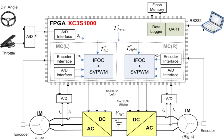
The developed propulsion system, depicted in Fig. 1, aims to control an Electric Vehicle with 2 induction motors, through a single FPGA chip. The energy applied to the motors is regulated by a set of DC/AC converters, supplied by electrochemical batteries, and controlled by a XC3S1000 [8]. The most important modules in the FPGA are the two Motor Controllers (MC), one for the right motor and the other for the left motor, coded in Verilog and running in parallel. Each MC is responsible for tracking the torque demanded by the driver, manipulating the PWM (Pulse Width Modulation) signals applied to the inverters. The MC algorithms are based on the well known indirect Field Orientation Control technique [10], containing a current loop control, a Space Vector PWM (SVPWM) generator, and modules for sensors interface, like encoders and analog to digital converters. The current loop control represents the innermost control loop of the whole system and is performed with a digital proportional-integral (PI) current controller. The motor currents are digitalized by an
analog to digital converter and sent to the FPGA through a high speed serial link. The final stage of AC motor control is commanding the power semiconductors to get the desired voltage and frequency. Due to high performance and its ease of implementation using digital logic, the Space Vector Modulation (SVM) has been a preferred PWM technique for the propulsion system. To perform tasks that do not need high speed, such as communications with supervision units, and data logger functions, a picoBlaze soft processor was included, using the logic primitive of the FPGA. For preliminary tests, a uniform torque distribution strategy has been used, with both MC receiving the same torque reference (Tleft = Tright), defined
by the throttle position. This simple strategy emulates the basic features of a single axis mechanical open differential, widely used in conventional vehicles.
III. MOTOR CONTROLLER A. Principles of Operation
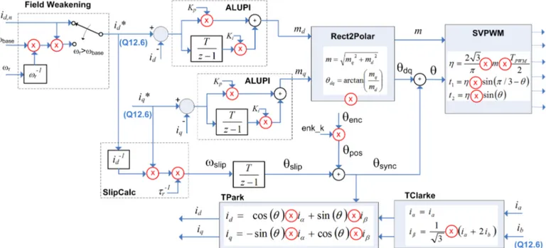
Despite the benefits resulting from the use of FPGAs on multi-motor control applications, some implementation issues arise due to the limitation of computational resources in FPGA. The multiplication operation is often used in control algorithms, and dedicated multipliers are valuable and limited resources in FPGAs. In Fig. 2 the main blocks used in each MC are presented, highlighting the multiplication operations performed by the indirect Field Orientation Control (IFOC) and SVPWM methods [10]. The MC starts by applying the Clarke and Park transformation (5 multiplications) to the
stator currents ia, ib in order to translate them to a coordinate
system which rotates in synchronism with the rotor flux vector.
These currents are regulated independently by two linear PI controllers (4 multiplications), the iq controller for torque and id
controller for rotor flux, generating the stator voltage reference in Cartesian coordinates (md, mq) which are converted to the
polar representation (|m|,θdq ) using the CORDIC (COordinate
Rotation DIgital Computer [9]) algorithm (1 multiplication used in output compensation). The final step is the transformation of the voltage reference vector to the stationary reference frame (|m|, θ) and apply it to the SVPWM to generate the pulses to be sent to the inverter (4 multiplications). Additional modules for field-weakening operation (2 multiplications), slip calculation (2 multiplication) and encoder angle (θenc) normalization (1 multiplication) are also included
in the MC. Counting all the multiplication operations, each MC needs 19 multipliers, or 38 multipliers for the 2 MC instantiated in the FPGA.
If a dedicated multiplier is used for each multiplication, the cheaper and smaller FPGAs (see Table I) do not meet the minimum computational requirements. For example, the XC3S1000 only has 24 multipliers, when 38 were needed to implement the 2 MCs. Furthermore, the use of FPGAs with more than 38 multipliers significantly inflate the cost of the solution (Virtex XC4VLX25) or unnecessarily increase the number of pins and the complexity of the package (XC3S2000 or XC3SD1800A), raising the printed circuit board cost.
To overcome this limitation, a multipliers sharing strategy was used, which can reduce the number of dedicated multipliers in the FPGA, and therefore the cost. This approach introduces a small latency in the execution of the algorithm, but tolerable since the execution rate of the MC is not very high. Normally, in electric traction applications, the current levels
are very considerable (in our prototype, 120A are normally applied to the motor), which impose limits in the maximum switching frequency to restrain the semiconductors energy dissipation. This switching frequency, typically below 20 kHz, constitutes the minimum execution rate of the MC. Since the FPGA main clock is equal to 50MHz, the MC algorithm can handle a maximum of 2500 latency cycles (equivalent to 1/20k = 50us) introduced by the multiplier sharing strategy (and other latencies).
In the following sections it will be presented the details of the resource sharing strategy, which allows us to reduce the number of dedicated multipliers from 19 to 11 and use a simple and low cost XC3S1000 to simultaneously control 2 induction motors.
B. Matrix multiplication - ALUMatrix2x2
TABLE I. MAIN RESOURCES AND SMALLER PACKAGES TYPE AVAILABLE IN THE SPARTAN 3[8],SPARTAN 3A-DSP AND VIRTEX 4
FAMILIES. Spartan Family Num. Slices Dedicated Multipliers Smaller Package Num. Pins XC3S400 3584 16 TQG 144 XC3S1000 7680 24 FTG 256 XC3S1500 13312 32 FGG 320 XC3S2000 20480 40 FGG 456 XC3S4000 27648 96 FGG 676 XC3SD1800A 16640 84 CSG 484 XC4VLX15 6144 32 SFG 363 XC4VLX25 10752 48 SFG 363
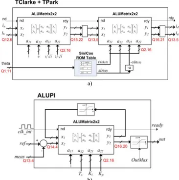
Some of the computing blocks of the MC, as the Clarke and Park transformation and PI controllers, can be formulated in a matrix representation. The implementation of these modules can be significantly simplified if an efficient computation module is available to perform multiplication of matrices by vectors. To take advantage of this fact, a dedicated computational module, designated as ALUMatrix2x2, has been developed, which performs the multiplication of a matrix, with 2 rows and two columns (2x2), by vector with 2 elements:
⎥
⎦
⎤
⎢
⎣
⎡
⎥
⎦
⎤
⎢
⎣
⎡
=
⎥
⎦
⎤
⎢
⎣
⎡
=
2 1 22 21 12 11 2 1x
x
a
a
a
a
y
y
Ax
y
(1)Normally this operation requires 4 multiplications and 2 sums. The ALUMatrix2x2 module only uses 1 multiplier, instead of 4. This is achieved by multiplexing the multiplier inputs, inserting a set of auxiliary registers to store intermediary results and including a finite state machine (FSM) to manage the calculations (see Fig. 3). Details about the FSM operation are omitted but can be easily inferred: acknowledge new data (signal nd), selects a11 and x1 signals, multiply, store multiplication result in the temporary register (ldtmp), selects inputs a12 and x2, multiply, perform sum, store output y1, and so on. In total, 15 latency cycles are introduced by the multiplier sharing strategy.
Since this computational block is reused in various MC modules, the bitwidth of the multiplier is adjustable by the parameter NBITS, to allow different quantization levels. For instance, the Clark and Park transformations and the PIs use fixed point (signed) format, with 18 bits (see Fig. 4), while the SVPWM module (see Fig. 5) only uses 13 bits.
C. Park and Clarke Transformation
The Clarke transform, in its matrix form, is given by:
⎥
⎦
⎤
⎢
⎣
⎡
⎥
⎦
⎤
⎢
⎣
⎡
=
⎥
⎦
⎤
⎢
⎣
⎡
b ai
i
i
i
3
2
3
1
0
1
β α (2)and the Park transform:
( )
( )
( )
( )
⎥
⎦
⎤
⎢
⎣
⎡
⎥
⎦
⎤
⎢
⎣
⎡
−
=
⎥
⎦
⎤
⎢
⎣
⎡
β αθ
θ
θ
θ
i
i
i
i
q dcos
sin
sin
cos
(3) The transformations (2) and (3) can be efficiently implemented reusing the ALUMatrix2x2 module (see Fig. 4a), presented in the previous section. The transformation (3) also requires the determination of trigonometric functions, which are obtained through two ROM tables. Note that the reuse of the matrix multiplication block, with resources sharing, reduces the number of dedicated multipliers from 5 to only 2, and introduces a 30 cycles latency (1.2% of 50us), perfectly acceptable given the minimum execution rate of the MC.D. PI Control
The regulation of iq and id currents is done by two PI
controllers, which, in its discrete formulation, can be represented by the following relationship:
[ ]
[ ]
[ ]
[ ]
⎥
⎦
⎤
⎢
⎣
⎡
⎥
⎦
⎤
⎢
⎣
⎡
=
⎥
⎦
⎤
⎢
⎣
⎡
+
+
k
e
k
x
K
K
T
k
y
k
x
p i s1
1
1
(4)Figure 3. ALUMatrix Module: multiplication of a 2x2 matrix by a vector using a single dedicated multiplier.
a)
b)
Figure 4. a) Clark and Park transformation; b) Proportional and Integral Controller, based on the ALUMatrix module ( all variables have fix point (signed) format, represented by the notation Qx.y - x bits for the integer
where e[k] is the error between the reference and the current measurement, x[k] can be interpreted as the integral of the error, y[k] is the output, Ki is the integral gain, Kp is the
proportional gain and Ts corresponds to the update rate of the
discrete system.
The PI control, like the transformations, can benefit from the use of the ALUMatrix module to decrease the number of computational resources in the FPGA (see Fig.4b). The error
e[k] is calculated by subtracting the reference from the
measure, (4) is implemented through the ALUMatrix2x2 block, two limitation blocks restrain the integration error and the output and a clock signal defines the update rate. Thus, the number of dedicated multipliers for the 2 PIs is reduced from 4 to only 2, introducing 15 cycles of latency.
E. SVPWM
The Space Vector PWM, is one of the main techniques used to control three phase inverters, allowing a 15% increase in the linear zone of operation and a low current distortion, compared with carrier-based modulation techniques [10], and was the modulation method used in this work. The module receives the normalized voltage vector reference, defined in polar coordinates (m, θ), and generates six PWM signals to be applied to the power semiconductors. The modulus of the normalized voltage vector is normally defined as modulation index, given by:
dc m
V
v
m
π
2
1=
(5)where v1m is the fundamental output voltage and Vdc is the DC
Bus voltage. The three-phase inverter is capable of generating 8 voltage combinations (100, 110, 010, 011, 001, 101, 000 and 111 where 1 represents that the top switch is on and lower switch is off, and 0 mean the opposite) . These 8 vectors, 6 active and 2 null vectors, form a hexagon on the stationary reference frame and can be defined as:
⎪⎩
⎪
⎨
⎧
=
=
=
−7
0
0
6
,...,
1
3
2
) 1 ( 3,
, n
n
,
e
m
n j n ππ
(6)The principle behind the SVPWM is based on the modulation of adjacent space vector for each sector. For instance, if the voltage vector reference lies in the first sector, during a switching period of time the inverter must apply the vector m1 and m2 during t1 and t2 and m0 and m7 during t0 and t7
times. A more detailed description of the SVPWM techniques can be found on reference [10].
The detailed view of SVPWM implementation is presented on Fig. 5. To simplify the calculations, only the formulas valid in the first sector are implemented. The identification of the sector (1 to 6) in which the voltage vector lies is straightforward because the voltage angle (θ) is known and the
sector can be easily detected, comparing the angle of the voltage vector with the 6 sector limits:
⎪
⎪
⎩
⎪
⎪
⎨
⎧
≤
<
≤
<
≤
<
=
º
θ
º
n
360
300
,
6
...
120
60º
,
2
º
60
0º
,
1
θ
θ
(7)Next, an equivalent first sector voltage vector (m1s, θ1s) is
calculated, rotating the input vector to the first sector, which is performed subtracting the original voltage angle by (n-1)*60 degrees, and maintaining the voltage modulus:
(
1
)
60
º
1 1−
=
=
n
m
m
s sθ
θ
(8)Note that, because the voltage vector is in polar coordinates, both the sector identification and voltage rotation are much simpler to perform than if the voltage vector was Figure 5. SVPWM implementation diagram (top); SVPWM simulation results, with fixed modulation index (m=0.5) and variable theta (bottom).
defined in the Cartesian coordinates. With the voltage vector in the first sector, the times t1, t2 and t0, which defines the “on
time” of the 2 active voltage vectors and the zero voltage, are calculated with the help of a simple trigonometric relationships, valid for the first sector:
(
)
( )
(
)
/
2
sin
º
60
s
3
2
2 1 7 0 1 2 1 1 1t
t
T
t
t
t
in
t
T
m
s s s s s−
−
=
=
=
−
=
=
θ
η
θ
η
π
η
(9)Like the previous modules, (9) was obtained using a multiplication sharing strategy, which enables us to reduce the use of dedicated multipliers from 4 to only 1, for each SVPWM instantiation. The trigonometric function was implemented with one ROM (Read Only Memory) table, with the address bus specifying the sine angle, and the data bus returning the function result. The t1, t2 and t0 times must be transformed in
duty cycles to be applied to each arm in the inverter. The duty cycles, which depends on the ti times, but also on the voltage
vector sector, are stored in the Compare Registers (CRi), which are obtained by multiplying the timer vector [t1 t2 t0]T by a matrix Mi, depend on the sector in which the vector voltage lies (see [10] for Mi definition). Because the coefficients of the
Mi matrix are restricted to zeros and ones, this multiplication
can be efficiently implemented with 6 conditional sums. Before generating the PWM signals, the CRi registers are shaped with a pulse elimination method [11], dropping pulses less than a minimum width (2 times the inverter deadtimes) to ensure the proper operation of the inverter when high modulation indexes are used. The final step in the SVPWM is comparing the CRi registers with a triangular wave, generated with an Up/Down counter, and apply the dead-times to the PWM signals.
In Fig. 5 some simulations results for this module are presented. It can be seen the evolution of the CR1 register for a fixed value of the voltage vector module m (defined as |V*|) and a variation from 0 to 4π in the vector angle θ (defined as
theta). In the zoom box it is shown a fragment of the triangular
wave, operating at 10 kHz, and the output PWM signals, which demonstrates the correct operation of the developed SVPWM. These simulation results were obtained with the ModelSim program, which provides a useful environment to develop test-benches and conduct several tests to validate the correct function of the developed modules.
One final word for the coordinates system used in the SVPWM. Most SVPWM implementations represent the voltage vector in the Cartesian coordinates (mα, mβ , in
stationary frame). In this work, we choose to formulate the SVPWM in the polar coordinates(m, θ) to be easier to evolve in the near future to an hybrid PWM method, like the one proposed by Malinowski [12], to reduce the switches’ losses of the power converter.
F. Other modules
The Cartesian coordinates (md, mq) manipulated by the
linear PI controllers, must be converted to a polar representation (|m|,θdq) to be compatible with the SVPWM
input format (see Fig. 2). This operation was carried out efficiently using a CORDIC algorithm, available from Xilinx [13], calculating the module and angle of the vector (md, mq) in
20 cycles.
The slip calculation, field weakening and angle normalization are implemented the same way as depicted in Fig. 2. The multiplier sharing strategy was not applied to these modules, because the reduction of multipliers obtained in the transformations, PIs and SVPWM modules was enough to reach our objective: include 2 MC in the XC3S1000. Nevertheless, in the future, these modules could also benefit from the multiplier sharing strategy.
TABLE II. RESOURCE UTILIZATION OF THE MAIN IPCORES Type Module Slices Mul. BRAM (MHz) FMax
Motor Control (MC) Curr.Control (2*ALUPI + Rect2Polar + …) 1012 6 1 92 SVPWM 316 1 1 86 TClarke + TPark 212 2 1 78 Field Weakening 59 2 1 125 ADC Interface 47 190 Encoder Counter 37 134
(Note: Design Tool: ISE WebPack 8.2.03i, Family: Spartan 3, Speed Grade: -5) TABLE III. RESOURCE UTILIZATION OF THE XC3S1000FPGA
Module Instances Num. Slices Mult. Motor Control (MC) 2 (44%) 3366 (92%) 22
Others 1 (17%) 1365 0 Total (%) (61%) 4731 (92%) 22
(Note: Design Tool: ISE WebPack 8.2.03i, Family: Spartan 3, Speed Grade: -5)
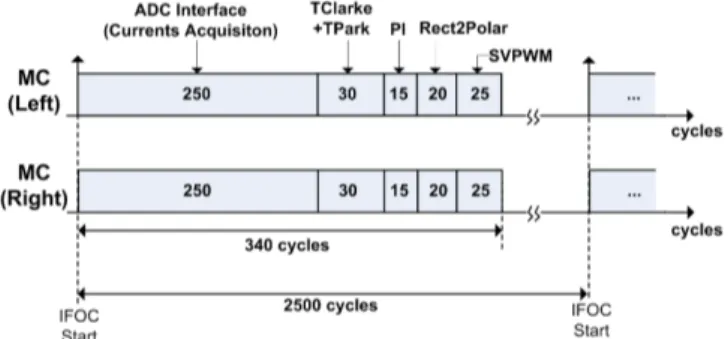
Figure 6. Latency introduced by the MC sub-modules (the main clock in the FPGA has a frequency of 50MHz, thus 2500cyces = 50us = 1/20kHz)
IV. LATENCY AND RESOURCE USAGE ANALYSIS A. Latency Analysis
Figure 6 shows the latency cycles introduced by the MC sub-modules. Before beginning the mathematical calculations, the MC must acquire the motor currents. Since the used FPGA does not have an internal ADC, the current measurement is done through ADCs (TI ADS7818) external to the FPGA and its value transmitted by a high-speed serial protocol. This acquisition process presents 250 latency cycles and represents the largest delay in the MC (73% of the total time). The MC computational blocks (Clark and Park transformation, PIs and SVPWM), introduces a latency of just 90 cycles. In total, the MC control cycles is performed in less than 340 cycles (6.8us), representing 14% of 2500 cycles associated with the MC minimum execution rate (20kHz). These results show that the latency introduced by the multiplication sharing strategy does not have a significant impact in the total execution time of the MC. Thus, there is some margin to implement more aggressive resource sharing methods to reduce the number of multiplier (and the FPGA cost). Moreover, albeit the MC modules have been specifically developed for electric traction applications, with the 20 kHz update rate limit, the low value of latency permits a significant increase in the execution rate (up to 147 kHz). This allows the MC modules to be reused in other industrial applications, where the demand for a high-bandwidth
control of torque and speed are much higher. Figure 6 also shows the parallel processing capabilities of FPGA, which allows multiple MC to run simultaneously, independently and without compromising the performance of other modules.
B. Resource Usage Analysis
Table II presents the resources utilization of the main sub-modules that compose the MC. An important factor that contributes for the resources usage is the variables resolution: the transformations and the PI Controller modules use fixed point arithmetic with 18 bits resolution (12 for the integer part and 6 bits for the fraction part) and the CORDIC and the SVPWM use 13 bits resolution. Note that, due to the multiplier sharing strategy adopted in this work, the total number of dedicated multipliers for each MC is reduced from 19 to only 11.
Table III shows the summary of the total resources utilization in the XC3S1000 FPGA used in this work. The two Motor Controllers instantiated in FPGA require 44% of the slices and 92% of the dedicated multipliers available on the chip. Although there are a considerable number of slices available, the low number of free multipliers prevents the inclusion of additional MC, which presents a restriction for future improvements. For instance, if an additional in-wheel motor is included in the vehicle, an FPGA with a greater
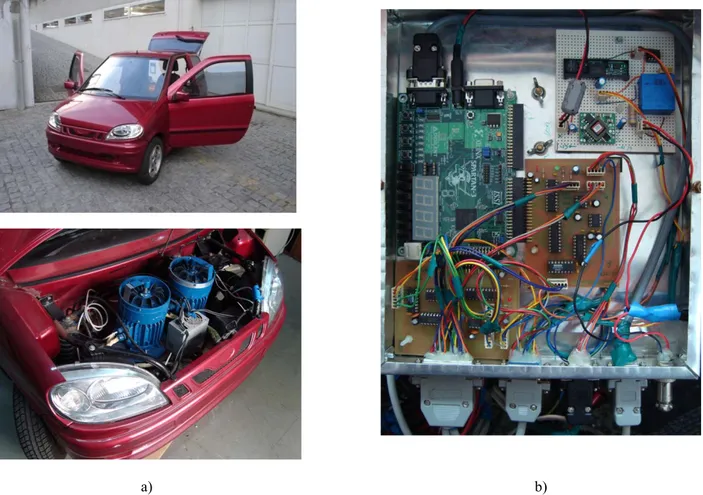
a) b) Figure 7. Multi-Motor Electric Vehicle prototype: a) chassis overview, with 2 AC induction motor coupled to the front wheels; b) FPGA Control platform based
number of multipliers (or a more aggressive sharing strategy) must be applied to allow further instantiations of MC in the chip.
In addition to the MC, there are also others modules to perform auxiliary functions such as datalogger, RS232 communications with the supervisory unit, electronic protections, etc., which consume 17% of the FPGA area.
V. EXPERIMENTAL RESULTS
The Faculty of Engineering of the University of Porto, in cooperation with some Portuguese firms, and under financial support of FCT (Foundation for Science and Technology), developed a multi-motor electric vehicle, named uCar (Fig. 7). In the context of this research a conventional MicroCar, Virgo model, was transformed in a multi-motor electric vehicle, composed with two, low voltage, 2.2kW three-phase cage induction motors (26V, Δ, 63A and 1410 rpm), coupled to the front wheels, and a set of four 12V lead acid batteries (105Ah) in a series configuration. To control the 2 DC/AC converters a single FPGA XC3S1000, based on the Digilent Spartan 3 Starter Kit, has been used (Fig. 7c). The FPGA board contains a set of useful peripherals (50MHz clock, expansion pins, Flash and RAM memory, etc.) and was expanded with 2 additional circuit boards. These boards contain ADCs peripherals (TIADS7818 and TIADS7848) to digitalize analog signals, such as currents, voltage, throttle signal, etc., which are essential for the control algorithms and for the 3.3V/5.0V and 5.0V/3.3V logic converters.
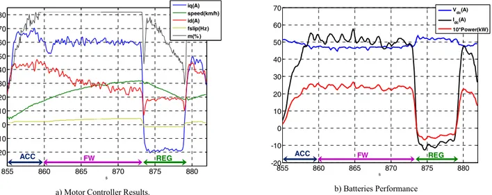
Preliminary experimental results, demonstrating the basic operation of the MCs, were acquired with the FPGA embedded datalogger, which records the evolution of mechanical variables (motor speed), energy source status (voltage and current) and the FOC controller variables (iq, id, motor slip, and
modulation index m) throughout the test. In Fig. 8a it can be seen the motor controller performance during a straight line test. During the initial acceleration the driver requests maximum torque and the currents iq and id are maintained in
their maximum values, producing an acceleration of 2.2km/h/s. When the EV reaches 18km/h the motor voltage saturates at 83% and id current (“flux” current) is reduced to allow the
vehicle to operate in the constant power zone. During this period each motor consumes, approximately, 2.5kW. After reaching 30km/h the driver requests a reduction in the vehicle speed and a negative iq current (“torque” current) is applied to
produce regenerative braking, converting 500W from kinetic to electrical energy (Fig. 8b), emphasizing one of the most promising features in EV: energy recovering during braking.
VI. CONCLUSIONS
In this paper, we explored the FPGAs parallel processing power to control two motors applied to an electric vehicle. The IFOC and SVPWM algorithms, used on the electric motor's control, need a considerable amount of multiplications. To reduce the number of dedicated multipliers on the FPGA, it was implemented a resources sharing strategy built on an efficient computational block for the multiplication of a 2x2 matrix by a vector. This strategy made it possible to reduce the number of multipliers from 38 to only 22, which allowed the use of a simple XC3S1000 FPGA to control 2 three-phase induction motors. The experimental results show the correct functioning of the proposed system.
The presented propulsion only looks at the motor control layer, but in future works we want to include additional layers of control on the FPGA, such as traction control, active torque distribution and stability control, to improve the multi-motor electric vehicle's security and handling.
REFERENCES
[1] Y.Y. Tzou and H.J. Hsu, “FPGA Realization of Space-Vector PWM Control IC for Three-Phase PWM Inverters”, IEEE Transactions on Power Electronics, Vol. 12, No. 6, 1997
[2] M. Naouar, E. Monmasson, A. Naassani, I. Slama-Belkhodja and N. Patin, “FPGA-Based Current Controllers for AC Machine Drives – A
855 860 865 870 875 880 -20 -10 0 10 20 30 40 50 60 70 80 s iq(A) speed(km/h) id(A) fslip(Hz) m(% ) ACC FW REG
a) Motor Controller Results.
855 860 865 870 875 880 -20 -10 0 10 20 30 40 50 60 70 s Vdc(A) Idc(A) 10*Power(kW) ACC FW REG b) Batteries Performance
Figure 8. Experimental results during acceleration, field weakening and regenerative braking during a straight line manoeuvre (only results from the left motor are depicted, right motor has similar performance).
Review”, IEEE Transactions on Industrial Electronics, Vol. 54, No.4, 2007
[3] E. Monmasson and M.N. Cirstea, “FPGA Design Methodology for Industrial Control Systems—A Review”, IEEE Transactions on Industrial Electronics, Vol. 54, No.4, 2007
[4] “Accelerator Drive Design Platform - IRACS201 datasheet”, International Rectifier, 2003
[5] T. Takahashi and J. Goetz, “Implementation of complete AC servo control in a low cost FPGA and subsequent ASSP conversion”, Nineteenth Annual IEEE Applied Power Electronics Conference and Exposition, 2004
[6] J. U. Cho, Q. N. Le and J. W. Jeon, “An FPGA-Based Multiple-Axis Motion Control Chip”, IEEE Transactions on Industrial Electronics, Vol. 56, No. 3, 2009
[7] K. Tazi, E. Monmasson and J.P. Louis, “Description of an entirely reconfigurable architecture dedicated to the current vector control of a
set of AC machines”, The 25th Annual Conference of the IEEE Industrial Electronics Society, 1999.
[8] “Spartan 3 FPGA Family –Complete Datasheet”, XILINX, June, 2008 [9] Ray Andraka, “A survey of CORDIC algorithms for FPGAs”,
ACM/SIGDA 6th International Symposium on Field Programmable Gate Arrays, Feb. 1998
[10] M.P. Kazmierkowski, R. Krishnan and F. Blaabjerg, “Control in Power Electronics – Selected Problems”, Academic Press, 2002
[11] A.M. Hava, R.J. Kerkman and T.A.Lipo, “Carrier-based PWM-VSI overmodulation strategies: analysis, comparison and design”, IEEE Transactions on Power Electronics, Vol. 13, No. 4, 1998
[12] M. Malinowski, “Adaptive modulator for three-phase PWM rectifier/inverter”. In Proc. EPE-PEMC Conf. Kosice, 2000